By Debra Vogler, senior technical editor
June 6, 2011 — SuVolta is tackling the low-power challenge of mobile SoC devices with its PowerShrink platform and undoped, deeply depleted channel (DDC) technology.
Fujitsu is the first licensee of this technology for its 65nm ASSP, ASIC, and COT product lines. The companies have verified the technology and begun joint development activities for commercialization, targeted to be available in the second half of 2012.
 |
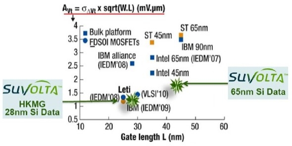
| Figure 1. SuVolta Vt variation reduction in perspective, 65nm bulk CMOS Vt variation. (SOURCE: F. Andrieu, et al., Solid State Technology, 11/10; with SuVolta data added.) |
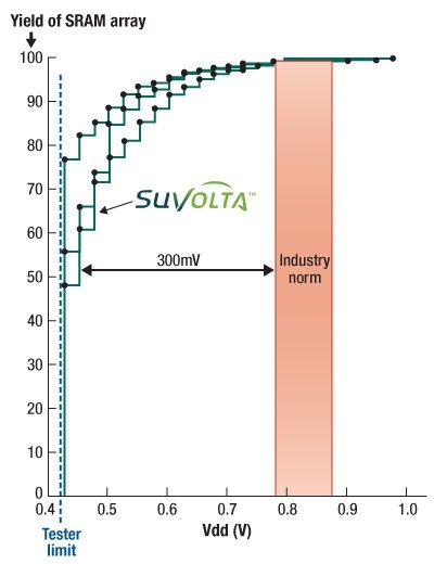
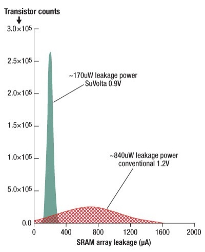
Scott Thompson, SuVolta CTO/SVP of technology, says DDC technology produces high performance at low voltage because it enables inversion charge to move from source to drain without scattering with dopants. The undoped channel and screening regions provide threshold voltage variation as good as the best fully-depleted SOI (FDSOI) and fully-depleted FinFET research devices (Fig. 1), explained Thompson. In this podcast interview, Thompson provides an in-depth technical discussion of DDC and PowerShrink. Other data reported by the company includes the technology’s exceptionally low-voltage SRAM operation (Figs. 2 and 3).
|
Listen to Scott Thompson’s podcast interview here: |
 |
| Figure 2: Exceptionally low-voltage SRAM operation. (SOURCE: SuVolta) |
Regarding scalability of this technology to nodes below 65nm, Thompson said that no circuit tricks are needed to make this technology work at low-voltage between 65 and 14nm. Because power dissipation is dominated by the low Vt edge of the distribution, the smaller the variation (σVt), the less leakage power.
 |
| Figure 3: 5× lower SRAM leakage demonstrated. (SOURCE: SuVolta) |
Just as significant as performance considerations may be the cost issues inherent in the company’s compatibility argument: the technology is compatible with: 1) existing fab infrastructure (no new equipment or materials); 2) existing CMOS process integration (no added masks); 3) legacy IP (with at least $1 billion invested in legacy IP by the industry, as estimated by SuVolta, this is not a trivial consideration); and 4) existing EDA flows (standard SoC design flows and tools).
Subscribe to Solid State Technology/Advanced Packaging.
Follow Solid State Technology on Twitter.com via editors Pete Singer, twitter.com/PetesTweetsPW and Debra Vogler, twitter.com/dvogler_PV_semi.

