(July 8, 2010) — Scientists from Singapore A*STAR’s Institute of Materials Research and Engineering (IMRE), University of Cambridge (UK) and Sungkyunkwan University (South Korea) have created metallic lines so thin and smooth that they can only be seen through powerful electron microscopes. This research will be published in the July issue of Advanced Functional Materials, a full-paper materials science journal.
 |
 |
|
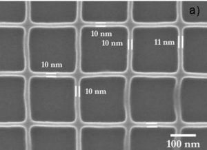
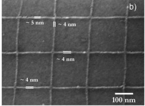
Nanoscale lines of (a) copper naphthenate and (b) copper after hydrogen reduction showing size reduction by about 50%, to make the metal lines. |
|
At 7nm line widths, their line width roughness (the variations in thickness along the line itself) stands at 2.9nm, a value below the 2010 target of 3.2nm and closer to 2011’s target line width roughness of 2.8nm, indicated in the International Technology Roadmap for Semiconductors (ITRS).
The ability to create such distinct lines and patterns on a sub-10nm scale level is essential in the further miniaturization of electronic components. Rough patterns and lines result in poorly made, energy-inefficient devices. The process is very delicate and precise because of the scale at which the work is done. For comparison, the width of the average human hair is 100µm, which is about 14,000× the width of a single 7nm-wide metal line.
“Our thin, unbroken and smooth lines are important in ensuring the efficiency of ever shrinking electronic devices and may lead to more powerful processors. Furthermore, our work shows that continuous metallic lines as small as 4 nm are possible to make,” said MSM Saifullah, Ph.D., a research scientist with IMRE. The method could be potentially used to make interconnects, the highways that carry electrical pulses and data in extremely small integrated circuits (ICs). The smoother and uninterrupted highways lead to faster data transfer rates and less energy wasted in the form of heat.”
The novelty of the method was in the material and technique used. The current “lift-off” approach for making metal lines at this scale requires more steps, uses more materials and results in rough and often broken lines on a sub-10nm scale. The researchers used an organometallic material made up of a metallic and an organic component. Using a combination of electron beam lithography and subsequent gas treatment, the researchers were able to easily chip away the organic portions in a uniform manner, leaving the desired metallic patterns, in this case, thin metal lines.
| Material | Line width, nm (average) | Pattern height, nm | Aspect ratio | LWR (3LWRσ), nm |
| Copper naphthenate | 10 nm | ~75 nm | ~7.5 | 1.9 |
| Copper | ~5 nm | ~50 nm | ~10 | – |
“The published results testify to the cutting-edge nanotechnology research that is done in Singapore,” noted Professor Andy Hor, IMRE’s new executive director, who took the helm of Singapore’s materials research institute in June 2010.
“Our expertise in the area of nanopatterning is also a reason why we are driving a concerted effort for the industry to adopt technologies such as this into their manufacturing processes”, explains Hor. IMRE will be launching an Industrial Consortium on Nanoimprinting (ICON) on August 3, 2010, to encourage industry to take full advantage of the benefits that advanced nanopatterning has to offer.
The research on the metal lines will be featured on the inside front cover of Issue 14 (July 2010) of the Advanced Functional Materials journal.
The Institute of Materials Research and Engineering (IMRE) has built strong capabilities in materials analysis, characterization, materials growth, patterning, fabrication, synthesis and integration. R&D programs have been established in organic solar cells, nanocomposites, flexible organic light-emitting diodes (OLEDs), solid-state lighting, nanoimprinting, microfluidics and next generation atomic scale interconnect technology. For more information about IMRE, please visit www.imre.a-star.edu.sg
The Agency for Science, Technology and Research (A*STAR) oversees 14 biomedical sciences, and physical sciences and engineering research institutes, and seven consortia & centres, which are located in Biopolis and Fusionopolis, as well as their immediate vicinity. A*STAR supports Singapore’s key economic clusters by providing intellectual, human and industrial capital to its partners in industry. It also supports extramural research in the universities, hospitals, research centres, and with other local and international partners. For more information about A*STAR, please visit www.a-star.edu.sg.

