January 13, 2009 – Attendees at this week’s Industry Strategy Symposium (ISS) have heard plenty of good economic news. Forecasters are predicting two or more good years of strong growth for the semiconductor industry amid a rebounding global economy. Analysts see growth in PCs, digital cameras, video recorders, DTV, servers, video games, and cell phones, along with strong growth in China and India.
Along with this buoyant optimism, however, comes a recognition that the semiconductor is undergoing a fundamental change in structure that will leave only a handful of companies producing devices at the leading edge. Bob Johnson, VP of research at Gartner, predicts that by 2014 there will be only 10 companies operating at the leading edge: 1-2 nonmemory IDMs, 4-5 memory companies, and 3 foundries.
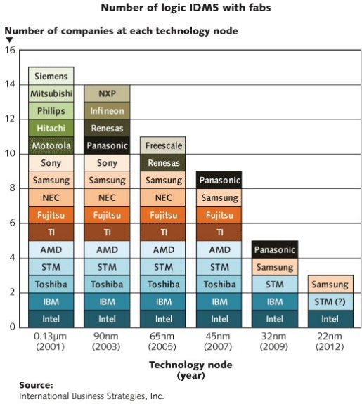
That sentiment was echoed by Handel Jones, CEO of International Business Strategies, who predicts "significant changes" over the next 5-10 years, both in terms of the structure of the industry and its cost structure. By the time the 22nm generation rolls around in 2012, he predicts there will be only three IDMs: Intel, Samsung and STMicroelectronics, and in terms of foundries working at 22nm, he thinks TSMC and GobalFoundries (which recently acquired Chartered Semiconductor) will be around. The fate of Samsung, which recently entered the foundry business, will depend on the success of their model, he said, adding that SMIC is an unlikely participant, and the capacity of UMC is "unclear."
 |
A similar situation exists in the memory market. "What we see today is a number of companies the DRAM business, in NAND flash and NOR flash business, but if you look out two to five years, you’re going to have one or two companies and that’s it," Jones said. Samsung will again be a major player, with a projected 50% of the DRAM market and 60% of the NAND flash market. "What we see now is Samsung moving ahead very rapidly and the others falling behind. The gap is widening," he said. Toshiba is a distant second, at least in NAND flash, where Jones expects them to garner 30% of the market.
One of the main drivers behind this consolidation is price pressure. "The semiconductor industry, even though it’s recovering from a revenue perspective, is not healthy from a profit perspective," Jones said. "Today, a relatively small number of semiconductor companies are making good profits. The market in 2010 will be comparable to the market in 2007 from a revenue perspective. Unit volumes though are up about 20-30%, so we’ve had an erosion of prices by 20%-30%. We’ve had some efficiency improvements but we’ve also seen a loss in gross profit margin and also a loss in operating income."
Jones believes this will result in "a significant restructuring" in which "only the top two or three companies in specific markets will survive." The drive from 32nm to 28nm will force additional consolidation, he added.
A similar type of consolidation is seen on the front-end semiconductor manufacturing equipment front (less so on the back-end test and packaging side). Gartner’s Johnson said that equipment suppliers will have "lost" about $116 billion in revenue between 2007 and 2014 due to the recession and record low levels of capital expenditures. This equates to about $17.4 billion in lost R&D.
This is happening at the same time when R&D costs are escalating due to a demand for continued shrinks, more advanced device structures and even a move to 450mm wafers (which continues to be a hotly debated topic).
Many believe this consolidation and funding gap has the potential to stop Moore’s Law dead in its tracks, perhaps at the 22nm generation. Jones said that the benefits of scaling, which he measures in terms of cost per gate trend, are not what they once were. The move to 90nm achieved a big cost decline in cost per gate, in part due to the transition from 200mm to 300mm wafers and associated productivity gains, he said. The move to 65nm brought "a fairly reasonable" decline, and then a small decline with 45nm and 32nm transitions. With 22nm, however, he said there actually will be an increase in the cost per gate — and without a reduction in cost per gate, many will question the need to move to the small feature dimension. "When you look at what applications drive the technology, if it is low-power (such as for handsets), that’s a cost-driven market," Jones said. "Maybe going to a smaller dimensions will not give you the required payback."
One bright spot: through-silicon vias (TSV) and 3D integration, which have the ability to increase functionality equivalent to a move to a new technology node. "In the past we were very cautious on TSV. We’ve become a lot more positive," Jones said.
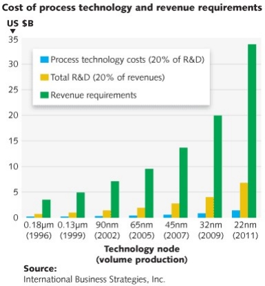
As a result of increasing costs, Jones also sees a reduction in the number of designs at advanced technology nodes. He said for a 28nm design, the costs can easily be in the $100M-150M range, and if you add software it can be up to $200M. "If you look at the normal metrics for R&D, you need 10× revenue from a production point of view. You then need $1.5 billion in revenue — and of course that happens in only a small number of products," he said. "After 22nm, the technology gets even tougher. The two year cycle is fading fast."
 |
Bob Bruck, VP of Intel’s technology and manufacturing group and GM of technology manufacturing engineering, added during a panel session that the number of fabs built each year has been declining: less than ten are expected to be built in 2011 and 2012, respectively (the majority of those being 300mm fabs). "Obviously this stuff is expensive," he said. The cost of a fab is about $4B, a pilot line costs $1B-$2B, and an advanced R&D process team can cost $500M-$1B. "You’ve got to have a large TAM to support this kind of investment, and you’ve got to have a pretty good gross margin on the product base to support this kind of investment," he said. "These types of dynamics are shaping this consolidation effect."
All this means the major fragmentation is widening between those that have and can afford the most advanced-node technology, and those who don’t/can’t, Jones said. "Those two segments are radically different and they’re going to get even more different." But despite that rift there’s still growth for those who choose not to push ahead to the advanced nodes. One group of companies is doing 45nm and now starting 32nm and 22nm, "we’re talking maybe 10 companies globally," he said. Another grouping of "hundreds of companies" are staying at wider feature dimensions, where "you actually have pretty good growth." In fact, he expects to see capacity shortages for some of these lagging feature dimensions in the next few years.

