May 20, 2010 – High-density through-silicon stacking (TSS) shows promise for very high-volume applications, but work still needs to be done to "tame" key issues in manufacturing, improve costs, and smooth out the supply-chain, said Matt Nowak, director of engineering in Qualcomm’s VLSI technology group, in a presentation at The ConFab in Las Vegas.
High-density TSS refers to small diameter (~5μm), high aspect ratio (~10:1) via-middle through-silicon vias (TSV), used in backside wafer interconnect processing of high-density (10s of μm pitch) tier-to-tier microbump connections, with >1000s of TSVs and microbumps per chip. Though there is "industry momentum" for high-density TSS in very high-volume applications, work still needs to be done to "tame" issues with design, thermal management, manufacturing costs, and test — e.g. through "judicious system partitioning" to clarify design and manufacturing supply-chain handoffs. There also are a variety of manufacturing flow options to consider: die-to-die, die-to-wafer, die-to-substrate, wafer-to-wafer, etc. — also thin before/after stacking, bump before/after post-fab processing, and tier-to-tier attach techniques such as microbump and Cu-Cu.
 |
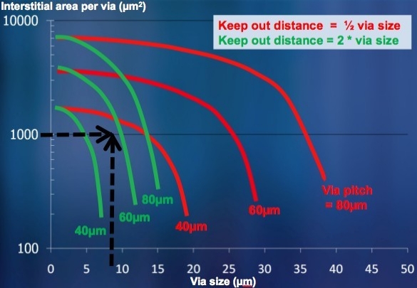
| Via size, pitch, KOD, and required interstitial area impact silicon cost. |
Cost in particular is currently a key challenge, he said, and there is no shortage of culprits, from incremental test cost to yield loss in both TSVs and microbumps, and incremental TSS process steps. Silicon area for TSVs is a key consideration as well, he pointed out, with via size, pitch, keep-out distance, and required interstitial area all impacting cost (see figure above). Possible cost-savings opportunities can be found in tweaking the laminate package size and number of layers, splitting large dies into two higher-yielding dies, and dividing into heterogeneous technology nodes.
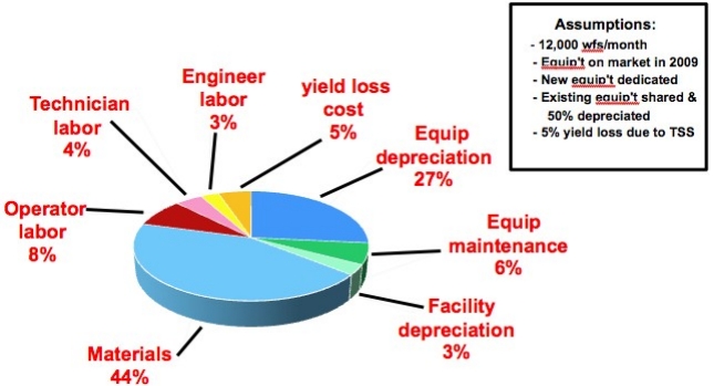
By far the biggest cost culprits are materials- & equipment-related, Nowak pointed out (see figure below). These can be addressed by improvements in materials (adhesives, underfill, molding compounds), equipment cost-of-ownership (throughput, uptime, tool configuration vs. volume), simplified process flow (e.g. eliminating B-RDL, replacing microbumps with lower-cost tier-tier bonding), and simplifying or eliminating temporary carriers.

He also urged standards for supply-chain handoff points, with specs and test methods to reliably manufacture TSS from multiple sources and processes, validated by experimental results (reliability, cost, yield, etc.). Target areas for initial standards include:
- Nomenclature/definitions
- TSV size, tier thickness, via fill material
- Tier-to-tier pin locations and assignments
- Key physical design rules
- Microbump and passivation materials properties and geometries
- Reliability test methods
- Metrology
- Thin wafer shipping

