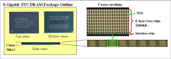
September 16, 2009 – Elpida Memory recently pushed vertical stacking of DRAM to new heights by connecting eight 1G chips using through-silicon vias (TSV), creating what it calls the world’s largest-capacity DRAM with ~8GB of storage.
The achievement doubles Korea’s Samsung Electronics stack of four chips, noted the Nikkei Business Daily. In the Elpida chip, each was etched with 1030 holes, using an internally developed method to position them with high precision and prevent distortions, the paper noted.
Reducing wire distance by connecting through the chip via TSV instead of with wire bonds enables faster speeds, lower power consumption (3/4 reduction in standby power vs. multichip/ packages and package-on-package), and smaller package size (1.3mm maximum, including an interface layer underneath). Future efforts may extend to multilayer TSV-enabled stacks combining logic and DRAM to create high-performance, low-power system chips, noted Elpida CTO Takao Adachi, in a statement.
 |
| (Source: Elpida) |
A manufacturing line has been set up in Elpida’s Hiroshima plant, using Akita Elpida’s package processing technology, the company said; the Nikkei Business Daily pegged this as a ¥5B investment for a 10,000 wafers/month TSV line . Sample shipments are slated to start by year’s end, with 16Gb (eight-layers of 2Gb) sampling in mid-2010.

