by Debra Vogler, senior technical editor, Solid State Technology
March 29, 2010 – As semiconductor industry evolves from planar scaling to 3D design to enable shorter interconnect lengths and higher I/O density along with more functionality, Applied Materials’ new Producer InVia dielectric deposition (CVD) system targets via-first and via-middle through-silicon via (TSV) integration applications. The new technology enables the deposition of the oxide liner film layer in high-aspect ratio (HAR) TSV structures.
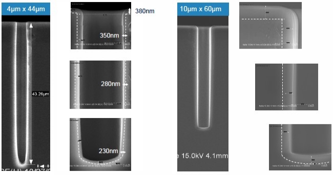
Because the via-middle application requires complete electrical isolation for device integrity, it has a thermal budget requirement ≤400°C, with conformality >50% of field oxide thickness over the full depth of the via (up to 11:1 A/R), sidewall thickness in the range 200nm to 1μm, and leakage current <2nA/cm2, among other requirements (see Figures 1 and 2). According to Applied’s global product marketing manager, Kedar Sapre, 80% of the company’s customers are doing a via-middle application, which, he notes, offers the greatest flexibility.
 |
| Figure 1. Coverage capability of the Applied InVia. (Source: Applied Materials) |
The new dielectric liner solution is implemented on Applied’s Producer GT platform, which the company says has the capability to process up to 8× more wafers/hr at less than half the cost, particularly when depositing very thick liners.
 |
| Figure 2. Conformality shown as aspect ratio vs. via opening. (Source: Applied Materials) |

