(September 13, 2010) — Package-on-package (POP) devices present some unique challenges with respect to the rework process: one of these is how to rework an underfilled package; also, these packages are prone to warpage. Lastly, the challenge of inspecting the area array devices can be overcome with highly trained personnel with experience in the BGA rework area. Bob Wettermann, BEST Inc., discusses rework solutions.
Stacking semiconductor packages suits various applications requiring smaller footprints, greater functional density, and higher performance. Consumer products using flexible package design include digital cameras, portable game players, GPS products, and smartphones. When these devices need to be repaired or upgraded or reworked, PoP packages require a robust, cost-effective, reliable rework process. This article discusses rework solutions.
PoP packages present some unique challenges with respect to the rework process: one of these is how to rework an underfilled package; also, these packages are prone to warpage. Lastly, the challenge of inspecting the area array devices can be overcome with highly trained personnel with experience in the BGA rework area.
Underfill
The rework of underfilled POPs is a major challenge as most of the underfill materials are epoxy-based. These epoxies need to be heated above their softening temperature (above 150°C) and along with this heat a mechanical force needs to remove this previously cured material. The material removal can be accomplished through high temperature vacuum extraction or hand tools, depending on the modulus of elasticity and underfill’s softening temperature.
The most commonly used underfill rework process begins with even substrate heating to a temperature above the underfill’s softening point. The package is mechanically gripped or pried with enough torque to break the fillet’s adhesions to the PCB. The chip undergoing rework is then heated above the solder reflow temperature to melt the solder connections and break the softened underfill. The device is removed from the PCB and residual solder and underfill cleaned off the substrate. Cleanup after chip removal removes any underfill, as well as excess solder on the substrate. This part of the process must be done with extreme care so as not damage the pads and adjacent components on the substrate. The site is then cleaned prior to inspection. Once substrate cleanup is complete, a new chip can be aligned, reflowed, and underfilled. The manual nature of this process — both heat and mechanical forces being used — results in less than a 50% yield in the best of cases.
 |
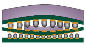
| Figure 1. Warped package-on-package (POP). |
Warpage
POP packages, due to their thin construction, are subject to warpage during initial assembly as well as rework. During the package-to-board placement process, if the lower package substrate flexes downward at its edges the solder ball contacts mating with the PCB can collapse to the point of collapsing together and creating a shorting condition (Fig. 1). Similarly, if the second-level package substrate warps in the opposite direction of the lower package, the solder will elongate and possibly separate.
Inspection and X-ray
Most contract rework houses or assembly houses have 2D X-ray as part of their normal non-destructive process control measures. By reviewing the ball diameters for consistency, problems in the rework process can be discovered. The trick is to make sure that the actual images being reviewed are all at the same layer. This can be difficult with a transmissive X-ray as the exact location of where the ball images show up in the Z-axis is difficult to confirm. All of the device layers are seen at the same time in the same X-ray image, so lower layers can be obscured by upper layers.
In some X-ray systems, oblique angle views (tilting the part or tilting the X-ray source) may be useful, but only to a limited extent. Layers placed further away from the X-ray tube will be seen as smaller than the closer layer; this phenomenon (known as geometric magnification) coupled with the different ball diameters of the different layers makes for very confusing X-ray images. Even when using a laminographic method (i.e., “slicing” of different x-ray image layers), there is not the resolution required to determine which ball sizes are to specification and which are not.
The challenges of inspection, part warpage and underfill removal without part all complicate the rework of POP devices. There are a few different methods being used to the rework process.
 |
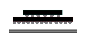
| Figure 2. Stacking one layer at a time method of POP rework. |
Different rework methods
There are two basics processes being used in the rework of POPs, namely: a “stack” of the multiple layers is pre-made and the device is then placed like a standard area array device (Fig. 2 “Stack one layer at a time”); or the first layer of the stack is placed onto the board and then the subsequent layer(s) of the stack are placed on top of the first. In either case, accurate and repeatable placement accuracy, the right materials, and tight process controls, are required to generate first pass yields over 95%.
Stack rework method. In the stack method, the devices are first assembled together and then placed as a single entity on the board location to be reworked. Starting with the package that is closest to the base package (the one that will be soldered to the PCB), solder paste is dipped into a reservoir to a depth of 40-50% of the ball diameter. The solder paste volume is controlled by ensuring that the reservoir is filled prior to each “dip” and that the depth to which the package is submerged is tightly controlled. Many rework stations can control this depth by having it “bottom out” in the reservoir. The nozzle then places the package on top of the base device. Finally, the stack is reflowed, cleaned and inspected. These steps are repeated for any subsequent packages that need to be placed onto the stack. Once the stack has been completed, the last step is attaching this “stack” to the PCB. Paste printing with either a removable stencil, or, for greater paste volume and prevention of shorts, a stay-in-place polymide stencil may be used to attach the stack to the PCB.
Layer rework technique. In this rework technique, each layer of the stack is individually placed one after the other beginning with the device being attached to the PCB, stacking the layers until all of the PoP elements have been placed. For the base layer, the PCB is paste-printed using either a peel-and-release type of stencil, or a stay-in-place polyimide stencil. Subsequent packages can have either paste flux or dipping solder paste applied, be aligned to the next layer in the stack, and then placed. Once all of the layers have been placed, the entire stack is reflowed. The benefit of this approach is that the die are only exposed to a single reflow and intermetallic growth in other layers is limited, increasing the probability of good device reliability.
Rework materials
There are several types of soldering materials that are recommended for use in the rework of POPs: solder paste, newly developed “dipping” pastes or fluxes, or paste flux.
Solder dipping paste used in the dipping process has different rheological properties than paste used for standard surface mount assembly. The dipping paste is lower in viscosity than that designed for printing or dispensing. Pastes with 75-80% metal content and type IV particles (20-38µms in diameter) work best for dipping.
Fluxes used in POP rework also have modified properties when compared to the standard BGA rework paste fluxes. The typical POP flux is a water-soluble, no-clean formulation containing a mild- to medium-active organic acid. When formulating tacky flux, suppliers must balance viscosity and elasticity so the material can be spread in a flat, even film for dipping. If the material is too thick, the film will have streaks or voids. If it’s too thin, the film won’t hold its shape or maintain an even thickness over time.
 |
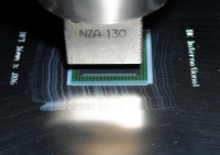
| Figure 3. Dipping paste used to attach one layer on to next. |
Dipping process for POPs
When “dipping” style fluxes and pastes are used in the rework of PoPs the rule of thumb is to dip transfer 40% of the ball diameter (Fig. 3). Compared to the printing process, dip transfer techniques transfer less solder paste volume. The dip method has a smaller process window compared to the printing process, and is therefore more susceptible to yield detractors, including poor dipping volume control for heavier parts and incorrect paste flux tack properties. The data implies that you are only likely to see an issue with the pick up PoP components from a dipping PoP flux tray if components are too heavy, if the vacuum nozzle is too small, or the flux has high tack properties.
In cases where underfills need to be applied underneath the device package, flux will not work. Since the lack of cleaning under the package prevents the underfill material from spreading completely there, flux is not recommended.
PoP rework recommendations
To overcome the numerous POP rework challenges, proper process techniques using good process control methods must accompany these materials.
There are several precautions you can take during POP rework to overcome warpage effects. One of the recommendations is to use a solder paste when placing the entire “stack” onto the board, or even in between the various layers. On the board location, this paste printing is recommended for maximum solder volume application. In between stacks, a “dippable” Fig. 3 solder paste can be used to increase the solder volume in the solder joint and therefore insure a greater process window. Finally, one can use a polyimide stay-in-place stencil that allows both a greater, more consistent volume of solder paste to be printed, and prevents the shorting of balls as a dielectric barrier is formed around each of the balls. These rework methods can be used to help overcome the negative impacts of POP package warpage during the rework process.
When attempting to rework a POP that has been underfilled, this very labor-intensive, low-yielding process many times makes the rework process undesireable. The epoxy and other material underfills require the use of both heat and mechanical force to remove. This combination ultimately either damages the part or the board, creating either more repair, or causing the board to be scrapped. Therefore, extreme dexterity of the rework operator is required to overcome this challenge.
There are challenges in inspecting a POP device after the rework process has been completed. For instance, some balls are “hidden” behind others in the x-ray image, or the inspector may be confused on which ball is on which layer. This problem can be somewhat mitigated by oblique angle views on the x-ray system. While not seeing all of the layers completely clearly, oblique angle viewing will have the propensity to show defects such as head in pillow (HIP) failures, and clearer indication of any opens.
 |
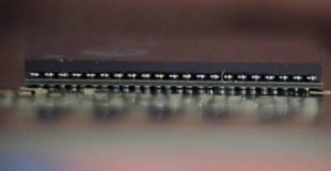
| Figure 4. POP post-rework. |
Conclusion
There are numerous rework challenges associated with POP devices. The problems of part warpage, proper inspection post-rework, as well as the rework of underfilled devices, are certainly challenging. They can be overcome to a great degree by using the proper materials; methods; and highly trained, skilled rework technicians.
References
[1] R. Boulanger, “Assembly Challenges of Package-on-Package,” Proc. of SMTA International Conf., 2006, pp.338-341.
[2] P. Wood, “Reworking Package on Package Components,” Proc. of SMTA International Conf. 2007, pp.363-367.
[3] L. Smith, M. Dreiza, A. Yoshida, “Package on Package (PoP) Stacking and Board Level Reliability Results,” Proc. of SMTA International Conf. 2006, pp.306-312.
[4] H McCormick, I. Sterian, J. Chow, M. Berry, J. Trudell, R. Cortero, “PoP: An EMS Persepctive on Assembly, Rework and Reliability,” Proc. of SMTA International Conf. 2008, pp.102-113.
Bob Wettermann received his BSEE University of Illinois, MBA DePaul University and is QC Manager at BEST, 3603 Edison Place, Rolling Meadows IL 60008; ph.: 1-847-797-9250; [email protected]
Follow Advanced Packaging on Twitter.com by clicking www.twitter.com/advpackaging. Or join our Facebook group


Nice topics you are discussed here. I mainly like Dipping process for POPs and X-Ray Inspection in the blog. Great research work you have done.