|
Executive Overview Performance requirements such as increased bandwidth, reduced latency, and lower power are driving the adoption of 3D-IC designs. What technology will be needed to make 3D-ICs a market reality at 45nm and below? While there are several options in development and production, one that is being touted as a way to build 3D-like structures relatively quickly is the use of silicon interposers—a double-sided die with no active devices that is used to connect one active die to another. Silicon interposers are being used to stack chips side-by-side, allowing designers to put dies next to each other in a high-bandwidth, low-latency configuration. However, while they provide a way to realize many of the benefits of 3D-ICs with fewer design and production issues, silicon interposers still pose new challenges for designers and manufacturers alike. |
Matthew Hogan, Mentor Graphics, Wilsonville, OR USA
A complete 3D-IC implementation is usually envisioned as a stack of active chips using through-silicon vias (TSV) to connect through each chip down to a package substrate. TSV designs represent a convergence of the SoC and SiP disciplines, providing designers the means to significantly increase the bandwidth between the logic chip and the memory (especially with wide memory interfaces) that can’t be achieved with bond wires, as well as the ability to mix and match dies that not only use different process nodes, but also different manufacturing technologies (SiGe, SOI, CMOS low voltage, CMOS high voltage, BiPolar, GaAs, etc.). The ability to combine different dies in a single stack, while not new, allows design houses to focus on their core design strengths, and acquire needed functionality (e.g., memory, RF transmitter) from specialist companies who can provide high-quality, proven die. What is new with 3D-ICs is the ability to place those connections in a dense array, without the strict perimeter constraints imposed by an equivalent wire-bonded design.
 |
|
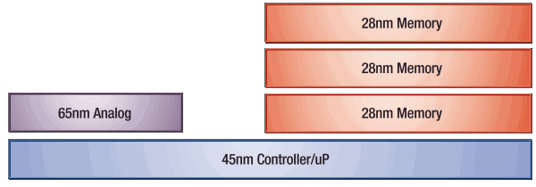
Figure 1. Stacked chip design. |
Utilizing stacked chips, particularly in memory-intensive designs, allows designers to stay at today’s "reasonable" process nodes for each die and derive the benefit of proven volume manufacturing processes. For example, if designers want to add memory to an existing design, they can simply add memory on a TSV die, and go "up" (Fig. 1). This flexibility lets engineers easily create variations of a design just by adding more memory to the stack.
However, TSVs used in active silicon have their own performance and production issues, making full 3D-IC implementations problematic. Of particular concern for a full 3D-IC stack is the issue of thermal reliability, particularly in high power configurations. Stacked dies can’t easily dissipate heat in the same way a single die does (through the use of a heat sink covering the largest surface area), which results in performance degradation and/or early failure. Minimizing heat production and/or controlling and dissipating heat effectively and economically is a challenging design and implementation issue for these structures.
In an active die, the physical size of a TSV (15-30µm diameter) is very large compared to the transistors that surround it (20-40nm). This significant difference in scale has a profound effect on routing, cell placement, and transistor stress (to name a few), all of which become a challenge when designing with TSVs in an active die. While creating space around the TSV can help alleviate these factors, that technique must be balanced against the resultant reduction in area available for transistors that provide the functionality of the device.
Alternative 3D technology
An alternative approach to a full 3D-IC stack is to place active dies on a passive silicon interposer, which in turn is placed on the package substrate. Silicon interposers with TSVs offer a way for designers to achieve the benefits of chip-scale connected configurations, without having to confront the issues currently presented by a full 3D-IC implementation through active silicon. The use of a silicon interposer is often referred to as a 2.5D-IC.
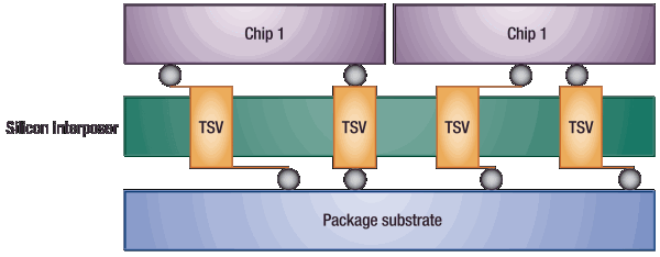
By using a silicon interposer, designers keep the circuitry of each active chip internal to the device package, reducing the need for HBM (human body model) electrostatic discharge (ESD) protection circuits and guard rings. Using a silicon interposer also makes it easier to "mix and match" active chips by using the interposer as a "rewiring loom" to connect chips without the need to specifically design them for interface compatibility (Fig. 2).
 |
|
Figure 2. Using a silicon interposer allows for signal remapping from one active chip to another without requiring customized designs. |
Silicon interposers are seen by some as a pragmatic building block in the evolution of 3D-IC technology. They are often used in high performance applications with single stacked devices (flip-chips) that allow for generous thermal dissipation using traditional techniques. Silicon interposers also provide a variety of additional benefits:
- Dies are created by a single source (no outsourcing to third party suppliers)
- Reduced ESD protection requirements for die-to-die connections through the interposer
- Drivers (transistors) need not be as large, because they’re not driving wirebonds to on-board (PCB) connections
- Heat buildup experienced in full 3D-IC designs may be avoided/minimized
- Process requalification is eliminated, because each die can be manufactured at a proven node without a TSV through the active silicon (for single stack configurations)
Looking ahead
For optimal package-aware chip design, questions must be asked and decisions made early in the design process. Is the connectivity created with the silicon interposer assembly the connectivity that you want? More specifically, when you have multiple dies sitting on top of the silicon interposer, how do they interact with each other? Will your power delivery match your performance requirements? Without the "right" answers to these questions, designers may not be getting the benefits this technology is intended to provide.
Standards are beginning to emerge for interposer size and pitch needed to meet performance standards. JEDEC recently announced that several of their standards committees are focusing on the development of 3D standards for stacked devices and mixed technology ICs [1]. The 3D-IC Alliance has released the Intimate Memory Interconnect Standard (IMIS) to standardize vertical interconnect requirements [2]. However, standards development may be hindered by some who perceive the interoperability of required technologies as a competitive disadvantage. Independent development and potentially conflicting solutions are always a risk.
Chip designers also need to decide how best to connect third party die that will require additional information. For example, to effectively use bare memory die, the micro-bump pad sites for each of the dies need to be aligned so the connectivity from one die can be traced through the passive silicon interposer and connect to the correct location on the other active die. Without knowledge of the physical interface, designers cannot effectively design the silicon interposer to connect with the die. However, information such as pad interfaces of an independent die is typically not a standard deliverable used in the design of another chip. Determining what information is needed and developing standardized methods of providing it will be needed.
From a design and verification standpoint, however, the good news is that extensive retooling is not needed. Many existing tools can be incrementally extended to handle 3D-IC design [3]. Incremental capabilities will be added to existing tools for coarse grain partitioning of designs, such as that of memory on logic, or other cells from one die to another. Fine grain partitioning, where the logic of a cell is partitioned over multiple dies, is probably only valid for very specific architectures at this time. The primary limiting factor is the manufacturing capability of the foundries. With a TSV being such a large structure compared to the transistors and other vias in the circuit, it remains a very deliberately placed object. When a TSV is small enough, with fine enough placement pitch to become a ubiquitous circuit element, then fine grain partitioning becomes significantly more viable.
Conclusion
3D-ICs are moving from theory (and a decade of hype) into reality. While challenges remain, there is little disagreement that 3D-ICs provide solutions to performance issues being encountered at the most advanced nodes. Silicon interposers were once viewed as an "interim" technology to help designers realize many of the benefits of 3D architecture, while delaying the most difficult production issues associated with TSVs. They now seem set to stay as a valid alternative implementation to full 3D-IC designs, at least for some market segments, and will become an integral part of future design architectures for others.
References
1. "JEDEC Announces Broad Spectrum of 3D-IC Standards Development," March 17, 2011; http://www.jedec.org/news/pressreleases/jedec-announces-broad-spectrum-3d-ic-standards-development
2. "First Standard For 3D Chips," July, 2008; http://www.3d-ic.org/documents/IMIS_Press_Release.pdf
3 M. Hogan, D. Petranovic, "Robust Verification of 3D-ICs: Pros, Cons and Recommendations," 3D System Integration, 2009. 3DIC 2009. IEEE Inter. Conf., vol., no., pp.1-6, 28-30 Sept. 2009doi: 10.1109/3DIC.2009.5306522
URL: http://ieeexplore.ieee.org/stamp/stamp.jsp?tp=&arnumber=5306522&isnumber=5306519
Biography
Matthew Hogan received his BEng from the Royal Melbourne Institute of Technology and an MBA from Marylhurst U. and is a Calibre Marketing Engineer for Mentor Graphics, 8005 SW Boeckman Rd, Wilsonville, Oregon 97070; ph.: 503-685-7065; email [email protected].
More Solid State Technology Current Issue Articles
More Solid State Technology Archives Issue Articles

