January Kister, Microprobe
March 1, 2011 — Consumer demand for ever smaller wireless and mobile communications appliances with increased functionality is driving the design and production of increasingly complex semiconductor devices. This trend is fueling the need for more advanced probe cards capable of accurately and cost-effectively testing complex ICs. According to the ITRS roadmap [1], pitches in the system-on-chip (SOC) market will continue to shrink with today’s 130µm full-grid array pitch configurations, shrinking to sub-100µm in 2016. In addition, the latest through silicon via (TSV) technology is scheduled to require sub-50µm pitch in full-grid arrays within the next three years.
As IC layouts shrink, corresponding wafer test probes must shrink too. This means that the resulting reduction in a wafer probe’s cross-sectional area lowers the amount of current an individual probe can deliver to the chip. To help lower the current-per-probe requirement, chip designers must incorporate a higher number of power/ground probes per chip to achieve the ITRS-specified 0.5Amp/probe.
In a wafer test production environment, however, the actual transient current consumption in flawed sections of the chip can be significantly higher than 0.5A/probe. As a result, probe card suppliers must provide probe cards with a current carrying capability (CCC) of ~1.0Amp level per probe to ensure production robustness. In this article, Kister examines the variables that impact CCC during wafer test, and describe an optimal probe design with a composite metal structure to address the 1.0Amp CCC requirement.
Defining a wafer probe’s current carrying capability
When an electrical current passes through a probe during wafer testing, it heats the probe through a process known as Joule (or I2R) heating. Some of this heat dissipates through conductive and convective heat transfer to the wafer, the space transformer, probe card support mechanicals, and the ambient air.
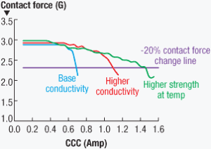
With a sufficient increase of current flow through the probe, the heat generated will exceed natural heat dissipation and probe temperature will increase. Eventually, the probe’s temperature reaches a critical value at which mechanical strength diminishes and plastic deformation begins (Fig. 1). This decreases contact force, which adversely affects electrical contact resistance. This, in turn, can generate unreliable test readings and wafer yield loss.
SEMI guidelines specify that the maximum allowable loss of contact force due to current passing through a deflected probe is 20% (Fig. 1) [5]. This specification, however, is typically measured one probe at a time and does not take into account probe-to-probe spacing or wafer chuck temperature, which is very important in wafer test. In addition, since the traditional current-carrying capability (CCC) spec is obtained through a one-time "static" test, it does not clarify how many cycles can be performed by the probe at current levels below the static CCC.
 |
|
Figure 1. Typical plot resulting from the SEMI methodology; a 20% contact force reduction marks the CCC spec. CCC improvement achieved through probe material conductivity (electrical and thermal) and high temperature strength increase. 75µm probe deflection. |
Variables affecting wafer-probe CCC
Wafer chuck temperature. An elevated wafer chuck test is typically used to accelerate and screen out chips suffering from "infant mortality." It is also commonly used while testing chips that are destined to work at elevated temperatures, such as automotive chips. Since a hot chuck increases wafer and air temperatures, it limits heat transfer from the probe body. Consequently, the probe runs hotter and reaches the CCC limit at lower current values. Figure 2 shows the characteristic reduction of contact force as a function of wafer chuck temperature. Here, the same probe that achieves 1.85Amp CCC at room temperature will sustain only 0.89Amp CCC at 180°C. The reverse occurs for the cold chuck test: the lower temperature of the wafer allows for greater heat transfer from the probe and therefore increases the probe’s CCC.
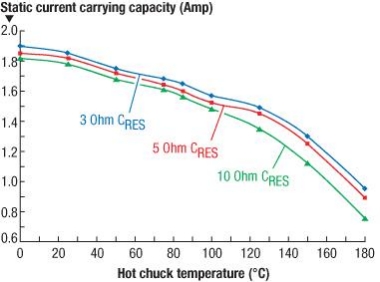 |
| Figure 2. CCC as a function of wafer temperature and contact resistance. Data for 75µm probe deflection. |
Probe tip contact resistance. A probe’s tip-to-pad contact resistance (CRES) build-up increases local heat generation through I2R and decreases local thermal conductivity. As a result, the CRES limits the heat transfer through the probe tip to the wafer. Figure 2 shows that at a chuck temperature of 150°C, the CCC will slip from 1.3Amp for a tip with 3.0ohm CRES to 1.12Amp for a tip with 10ohm CRES.
Wafer probe’s material properties. Material properties can affect a probe’s ability to perform as a high-current probe. Three key material properties impact CCC: bulk resistivity, mechanical yield and fatigue strength at elevated temperatures, and the probe tip’s metallurgy.
- Bulk resistivity: Low resistivity minimizes the temperature generated through heating [Temp=FN (Resistivity* current2)] and enables the probe to carry a higher current without reaching the critical temperature where its mechanical strength diminishes, as shown in Fig. 1 and Fig. 3.
- Mechanical yield and fatigue strength at elevated temperature: Materials that retain high mechanical strength at elevated temperatures can better support probe deflection stress as it heats up during probing. To maximize performance, it is desirable for the "CCC limiter," as shown in Fig. 3, to occur at as high a temperature as possible.
- Probe tip metallurgy: Because low contact resistance throughout the life of a probe card is essential for maintaining maximum CCC (Fig. 2, [3]), the probe tip’s metallurgy should be able to resist oxidation and prevent adhesion between the tip and IC pad/bump material, as these can increase contact resistance.
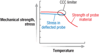 |
| Figure 3. Mechanical strength of typical spring metals diminishes rapidly past critical temperature, marked here as "CCC limiter." |
Probe pitch and pad layout. The proximity of neighboring probes plays a significant role in the heat transfer process during operation. A single probe that measures 1.05Amp CCC at room temperature will measure 0.95Amp when placed at 130µm pitch with another. When the same probe is surrounded by two other probes at 130µm pitch, its CCC will slip to 0.91Amp, as shown in Fig. 4. The reduction in CCC is caused by the mutual thermal effects between the neighbor probes. If the in-line configuration were changed to a 3×3 matrix at the same 130µm pitch, the CCC of the middle probe would be further reduced to 0.89Amp.
 |
| Figure 4. Influence of neighboring probe proximity on CCC at 130µm pitch. Color indicates temperature distribution. Red shows maximum allowable temperature. Plots achieved through FEA were confirmed through measurement. |
Probe geometry: Cross section/length. Slender probes perform worse than shorter probes with a larger cross-section, due to limited convective heat transfer from the middle of the length to the cooler wafer and space transformer components (Fig. 5). Conversely, shorter probes perform better due to the shorter distance to heat sinks and, therefore, offer a higher CCC.
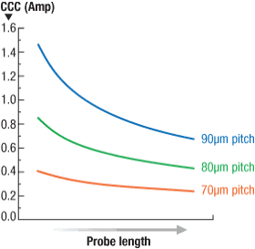 |
| Figure 5. Example relationship between probe CCC and probe length for geometries allowing 70, 80, and 90µm pitch in full grid array chip layouts. Note that the shortest probes here might not provide sufficient deflection for applications with large system planarity. |
Tradeoffs between probes’ CCC, probe defection range and inductance. The advantages of short probes include larger CCCs (Fig. 5) and smaller self inductance, which benefits applications where signal integrity and power/ground delivery is a concern. The disadvantage of short probes in wafer test is that they offer a smaller working deflection range, which limits their ability to work with wafers and test set ups with large planarity windows.
Conversely, slender and longer probes offer smaller CCCs, but often are needed when larger deflectability and lower contact force are required (such as when C4 bump height variation is >25µm window). The increased length, however, causes increased self-inductance.
Current duty cycle. Historically static CCC is measured using DC current. Most probes will reach their maximum critical temperature within 2s (Fig. 6). For shorter current-ON intervals one should consider duty cycle calculation to find equivalent DC current and, from there, the required CCC value.
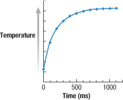 |
| Figure 6. Typical probe reaches its steady-state temperature in under 2s. |
Dynamic vs. static CCC spec. It is desirable for CCC specs to reflect the dynamic nature of wafer probe operation by being able to correlate current level to achievable number of probing cycles. Such information could be used to determine not only what current level a probe can carry one time, but also how many cycles a probe can sustain at various current levels below the static CCC (Fig. 7).
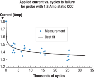 |
| Figure 7. Example of dynamic CCC test result correlating current to number of achievable probing cycles for a probe with 1.8Amp static CCC. |
Conclusion
To offer a robust production-worthy probe solution, probe card vendors need to consider all the trade-offs between mechanical and electrical probe card design characteristics.
Any optimal solution designed to address 1.0Amp/probe in sub-100µm array configuration challenges will require a composite probe structure such as MicroProbe’s Vx-RF probe (shown in Fig. 8). This multi-layer design allows for independent optimization of probe alloys with higher strength at elevated temperature, lower bulk resistivity, and low-wearing non-oxidizing contact tips to maintain highest CCC performance.
Short probe length designs with lower deflection windows can also be implemented for chips with a tighter flip-chip bump/pillar topology window. In addition, effective probe tip cleaning protocols become even more critical in maintaining the best CCC during production.
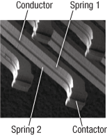 |
| Figure 8. Composite micro electromechanical system (MEMS) structure of MicroProbe Vx-RF probe optimizes conductivity, strength at elevated temperature and contact resistance performances |
References
1. "Wafer Probe Technology Requirements," ITRS, http://www.itrs.net
2. R. Holm, Electric Contacts and Applications, Springer, 3rd printing 2000.
3. M. Zeman, "A New Methodology for Assessing the Current Carrying Capability of Probes Used at Sort," IEEE SW Test Workshop 2010.
4. D. Gonzales, J. Kister, "Advancements in Performance of Buckling Beam Probes," South West Test Workshop 1999.
5. Standard Guidelines for Measurement of Current Carrying Capacity for Wafer Probe Wires and Needles, ISME Probe Council 2007
6. R. Kirby, H. F. Yan, "New Methodology for Probe CCC Characterization" Intel Corporation, South West Test Workshop 2004.
7. Incropera, DeWitt, Fundamentals of Heat and Mass Transfer, John Wiley and Sons 1985.
Jarek (January) Kister received an MS in mechanical engineering from the U. of Michigan, and a BS in mechanical engineering from Polytechnic of Silesia, Poland; he is also a graduate of the Advanced Management Program from the Haas School of Business at the U. of California, Berkeley, and is the VP of Engineering and CTO at MicroProbe, 617 River Oaks Parkway, San Jose, CA 95134, USA; ph.: 408 457-3900; [email protected]
Subscribe to Solid State Technology/Advanced Packaging.
Follow Advanced Packaging on Twitter.com by clicking www.twitter.com/advpackaging. Or join our Facebook group

