by Dr. Phil Garrou, contributing editor
January 6, 2010 – At the RTI 3-D Architectures for Semiconductor Integration and Packaging Conference in Burlingame CA, fresh off the 3D announcements of IBM and Samsung, several industry leaders focused on the imminent use of 3D interposers.
Arif Rahman, principle engineer at Xilinx, gave further details on their next-generation FPGA products that have been reported recently. When asked about their choice of a silicon interposer for their next-generation FPGA, he noted that "it appeared to be the most manufacturable way to offer product performance during our required timeline." The interconnect on the interposer is done at 65nm technology.
Douglas Yu, senior director of interconnect and packaging at TSMC, was likewise questioned about the foundry’s commercial commitment to silicon interposers (Xilinx is their customer), and he confirmed that TSMC will offer commercial silicon interposers.
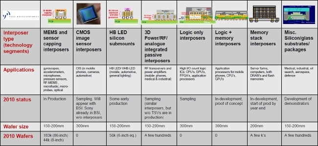
Jean-Marc Yannou , senior analyst at Yole Développment, pointed out that that silicon/glass interposers offer >10× more resolution and finer pitches than traditional organic substrates. Yole has identified eight categories of applications for silicon/glass interposers: MEMS; CMOS image sensors; LED submounts; RF with passives; logic; memory + logic; memory stacks; and miscellaneous.
 |
| 2010 status of 3D silicon/glass interposers. |
Songdong Cho, senior engineer in Samsung’s system LSI group, noted that mobile products will require more than 25GB/sec bandwidth and therefore "wide I/O memory with TSV appear to be the only solution." He described two platforms within the systems LSI group: Interposer and memory on logic.
Tzu Kun Ku, director of ITRI — which was on track to have its 300mm line baseline process completed by year’s end 2010 — described how interposers will reportedly reduce both system form factor and bill of materials simultaneously.


