(January 3, 2011) — The semiconductor industry’s ongoing discussion of "more Moore" and "more than Moore" at IEDM 2010 (12/6-12/8/10, San Francisco, CA) was continued with another invited paper presented by Leti researchers (paper #2.6, "Engineered substrates and 3D integration technology based on direct bonding for future More Moore and More than Moore integrated devices"). Laurent Clavelier, head of solar technologies department at Leti, discussed the significance of the paper with Debra Vogler, senior technical editor.
Listen to the podcast interview: Download (for iPhone/iPod users) or Play Now
According to Clavelier, the researchers used both Smart Cut and Smart Stacking technologies in their work. In the "more Moore" domain, the applications include SOI substrates as well as strained SOI, and the introduction of special layers, such as diamond. For one application, the group combined Smart Cut technology with 3D integration to create functions not feasible with monolithic integration.
 |
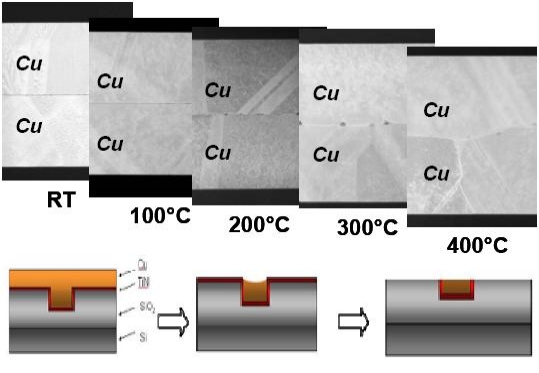
| Figure 1. Schematics of the CMP process (top) used for Cu/Cu direct bonding and TEM analyses (bottom) of the bonding interface as a function of temperature. SOURCE: Leti |
To evaluate such 3D integration, the group used a room temperature and atmospheric pressure direct Cu/Cu bonding that is fully compatible with classical copper back end of line (BEOL) and TSV silicon process (Figure). The paper noted that the polishing steps were customized.
Continue reading about this paper in "Leti on more than Moore for RF filters" in the ElectroIQ Semiconductors Center

