Category Archives: 3D Integration

Click to EnlargePete Singer
Editor-in-Chief

The potential benefits of 3D integration — where chips are thinned, stacked and electrically connected with through-silicon vias (TSVs) – are by now well known for stacking memory and for communication chips. It provides an alternative to scaling when it comes to cramming more functionality in a smaller space. It could also enable an increase in performance by shortening signal paths. It could in theory also provide a pathway for improved yield, by portioning large die into smaller, higher-yielding blocks.

So where are we on the 3D integration quest? We’ve assembled a variety of inputs in this issue (and on our website) to address that question.

First, Sesh Ramaswami of Applied Materials describes process equipment readiness for TSVs. He says that unit processes are now ready and integration is well advances for typical process flows and that it’s "ready for limited pilot production at several locations." For full volume production though, he said wafer cost is still a concern, noting that the combined costs of wafer-level thinning (bonding, thinning and de-bonding) and die-level processing (dicing, stacking, assembly and test) are in excess of 50% of the overall cost. He said industry standardization could help reduce the cost of materials and accelerate the release of higher throughput equipment in this area.

Next, researchers from EV Group, Andong National University (Andong, Korea) and the Korea Institute of Machinery & Materials, report on work aimed at reducing the temperature of copper-to-copper bonding processes while maintaining strong bonding energies (still a problem area). By optimizing experimental parameters, the researchers achieved sufficient interfacial adhesion with no voids, even with a short bonding time of 30min.

Integration with TSVs, however, is not the only technology path to higher levels of integration in 3D. Navjot Chhabra of Freescale describes and alternative based on the redistributed chip package (RCP), first introduced in 2007. He notes that RCP technology provides for package size reduction, high yields, a cost-competitive process on a 300 mm tool set, and ultralow-k compatability among other advantages.

In a fourth feature, consultant Vern Solberg compares 3D integration to system-on-chip approaches (while also noting the many advances in traditional packaging technology). He says that developing custom silicon designs for SoC will take time and often require substantial resources but will eventually yield positive returns – at least for high-end or long-running apps. For other products having a relatively short life cycle, 3D die stacking or package stacking will have a decisive advantage in both time and economics.

On our website, an online feature authored by DEK’s Jeff Schake, Mark Whitmore, Dave Foggie and Michael Brown (Weymouth, Dorset, UK), describes how some of the more challenging process conditions now being encountered in volume production require die-attach coatings as thin as 38µm to be applied to wafers that have been mechanically thinned to as little as 150µm. With such thin wafers, and the requirement for low coating thickness, the wafer-support tooling surface metrology is expected to have an appreciable impact on coating thickness control. Thinner wafers may more easily translate deviations through their more flexible structure. The article discusses the flatness characteristics of currently available wafer pallets, and describes an experiment to measure and compare the process performance achieved when depositing an adhesive onto a total sample of 45 150µm thick, 200mm wafers, using six different types of pallets.

Also on the web, find an analysis of 3D activity at SEMICON West, penned by packaging expert and blogger Phil Garrou, and a variety of video interviews, including one with Sesha Varadarajan of Novellus. Varadarajan says that capacitance issues must be overcome, and the PVD step must provide good enough coverage to properly apply copper. CTE mismatch can also cause issues.

In short, as Chhabra notes, the hurdles to 3D integration begin with the design and modeling infrastructure and continue with the need for process and materials development. Costs need to be decreased through improved yields and standardization and, ultimately, ongoing reliability concerns must be alleviated as well. One industry source at SEMICON West bemoaned the fact that cost targets were set so early and then said to be met, when in reality the technology has yet to be fully proved in volume production. That might be the biggest challenge moving forward: resetting cost per wafer expectations.

More Solid State Technology Current Issue Articles
More Solid State Technology Archives Issue Articles

Executive Overview

As fan-out technology production ramps and exposure to the technology grows in the industry, there is an interesting set of opportunities emerging. Although RCP technology can provide distinct advantages over both wirebond and flip chip single die packaging solutions, a closer evaluation of fan-out suggests that a more pronounced advantage is possible in the form of a multi-die, or system-in-package (SiP) solution. The RCP multi-die program is specifically designed to incorporate several of these advantages: heterogeneneous integration (die, passives, peripherals), system miniaturization, system performance, system cost, high speed in package computing, system flexibility (chip sourcing, integration), block testability, and a path to integrating with 3D TSV ICs.

Navjot Chhabra, Freescale Semiconductor, Austin, Texas, USA

Beginning in the 1990s and coming into its own in early 2000s, three dimensional (3D) through silicon via TSV IC technology has demanded a significant amount of attention. It became apparent as process and design rules continued to migrate down Moore’s law that the challenges of having robust materials and chip performance were becoming a significant concern. Some of the motivations driving the development of 3D IC and TSV technologies are the increasing on-chip, high-speed signal paths as well as utilizing optimum functional blocks within the chip design. While die-to-die interconnects address many of the device functionality challenges, a number of processibility and reliability concerns remain. The hurdles to 3D integration begin with the design and modeling infrastructure and continue with clear needs for process and materials development, decreasing costs through improved yields and, ultimately, alleviating ongoing reliability concerns.

Fan-out technology

There is another technology path emerging in the industry. Similar to the evolution of front-end wafer processing, package technologies are also evolving. Historically, the motivation behind the typical packaging roadmap has been driven by the need to meet decreasing package sizes (x,y,z), lower costs, increase performance, and provide different reliability requirements and thermal and electrical compliance. However, within each packaging category the challenges of meeting certain reliability grades and functionality still remain. Similar to the ‘red brick wall’ seen on the ultra-low-k material roadmap, wire bond technology is beginning to see that similar concern. As die technology keeps advancing and more functionality is required, the ability to route signals without impacting performance and cost is a great concern. While the overall die cost continues to decrease with advancing nodes, package costs are heading in the opposite direction.

In the 1980s, companies began the development of fan-out packaging technology. The idea was to eliminate the need for substrates and gold wirebond, two of the highest cost items in a package bill of materials while, at the same time, addressing some of the limitations of contemporary packaging. In 2007, Freescale introduced a fan-out technology called the redistributed chip package (RCP) built on a 300mm tool set. This specific technology is targeted at meeting the requirements listed below.

Package size reduction: ~30% size and thickness reduction vs. PBGA; package size and routability: one to six signal redistribution metal layers (RDL) and a package size ranging from 2x2mm, to as large at 40x40mm; yields: assembly yield comparable to today’s packages; a cost-competitive, high productivity, large area batch process that eliminates the package substrate and eliminates gold wire bonds/C4 bumps; high-performance package with electroplated copper interconnects, reduced electrical parasitics, improved device efficiencies, higher frequency response, and active structures in routing (shielding, inductors); ultralow-k compatible (<90nm MLM) and compliant with advanced silicon technology. Additional requirements are: lead-free, halogen-free, and ROHS compliant; single chip, multiple chip and embedded component capability; 3D IC enabling with system integration roadmap; certified to JEDEC/commercial/industrial level reliability; and meets or exceeds JEDEC requirements for solder joint reliability and drop test.

In early 2009, RCP achieved both commercial and industrial-level certification on multi redistribution layer parts with a range of package sizes. This technology is also well underway towards meeting automotive level requirements. With thousands of 300mm panels produced to date, yields continue to achieve benchmark levels.

Meeting the analog challenge

The use of RCP technology for digital applications was fairly straight forward, however, its adoption for analog applications had additional challenges. Not only were the end user requirements much more stringent, well beyond JEDEC commercial specifications but the electrical parameter tolerances were dramatically tighter. Process and design enhancements to the RCP technology provided the solution with the added benefit of enabling ~20% reduction in die size, which had a significant benefit to both chip performance and cost.

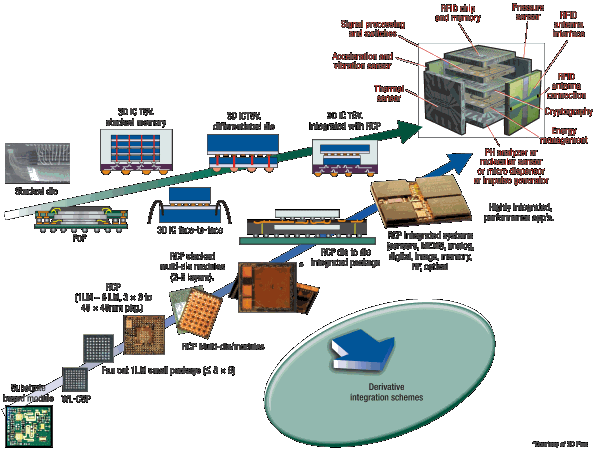
Freescale RCP multi-die systems currently being developed and sampled to end users are incorporating embedded surface mounted devices, discrete components, active RF features, shielding and thermal management structures while providing better system performance and shorter design cycles. For even more integration and performance, these two dimensional multi-die packages are being built in multiple, 3D planes and 3D integrated packages (Fig. 3).

Click to Enlarge
Figure 1. Convergence of 3D IC with 3D integrated packages.

As highlighted by the roadmap (Fig. 1), having the flexibility to design complex systems in a true system is a significant product and application enabler. Being able to integrate with the results of parallel development in 3D ICs provides the industry an appealing high performance, advanced integrated system. At this stage, the applications are extremely broad (Fig. 1).

Conclusion

Freescale is actively engaged in developing and providing RCP package solutions for medical applications, aerospace and optical devices, compact system solutions, advanced robotics and other technologies. Solutions involve the integration of discrete ICs ranging from two to more than 10 components along with added surface mounted devices. Packages in combination of 2D and 3D planes with thickness of < 0.5mm (3D stack) including solder spheres are being sampled. As the need to integrate MEMS devices and advanced memory for sensor applications expands, work is underway to develop modules merging both mechanical and electrical devices into single, highly compact modules.

Biography

Navjot Chhabra received his BS degree from Boise State U. and is the RCP development and operations manager at Freescale Semiconductor, 6501 William Cannon Drive West, MD OE:08, Austin, Texas 78735, USA; ph.: (512) 895-6470; email  [email protected].

More Solid State Technology Current Issue Articles
More Solid State Technology Archives Issue Articles

Executive Overview

Leading-edge applications are employing through silicon vias (TSVs) to satisfy the demand for devices to deliver more functionality faster in smaller dimensions, especially as consumer electronics become increasingly complex, compact, and energy efficient. In homogeneous or heterogeneous integration, similar or different chips are stacked top of each other and joined by vertical interconnects. Today, unit processes are ready and integration is well advanced, with "best known methods" for typical interposer, via middle, and via last flows ready for limited pilot production at several locations.

Sesh Ramaswami, Applied Materials, Santa Clara, CA USA

Accelerated data exchange, reduced power consumption, and much higher input/output densities are all enabled by 3D integration using TSV technology. Memory makers will implement homogenous TSV integration to produce stacked DRAM to boost the memory capacity per unit board area / volume. This method reduces latency and increases bandwidth between the memory and processor. Applications for heterogeneous integration include image sensors or communication chips in mobile devices. TSVs can also be used to improve yield. Large die can be partitioned into functional blocks (resulting in smaller die with higher yield) and integrated vertically atop each other or adjacent to each other on an interposer.

TSV schemes

TSV integration can be implemented in a number of ways. The simplest form is that of a silicon interposer through which vias have been etched and filled with metal (typically copper). Such interposers also have multi-layer damascene interconnects which connect die placed adjacent to each other. Interposers enable end-product designers to quickly integrate two chips without making a TSV within the individual chip. Most of the development to date has focused on via-middle and via-last, wherein the TSVs are created within the active die. In the via-middle scheme, the TSVs are etched after contact/transistor formation but before back-end-of-line (BEOL) processing. Via-last TSVs are created from the back side of a thinned wafer, creates the vias after BEOL processing.

Technology development and commercialization

Since the onset of the TSV "buzz" in mid-2008, the scope and content of the development program has been guided by a methodical evaluation of many aspects, including end-product requirements, market timing, industry eco-system, cost-effective process sequence integration, and manufacturing-worthy unit processes. This framework also provided common goals for collaboration among adjacent technologies to accelerate industry learning. Implementation risk is being mitigated not only through these collaborations but through joint prototype testing of process flows. The three overriding objectives that guide the integration work are: wide process window, capability to withstand processing on fragile bonded/thinned wafers, and overall cost of ownership of the fabrication flow.
Click to Enlarge
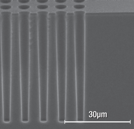
Figure 1. Etch technology demonstrates high resist selectivity, in situ dielectric open, combined with excellent profile control.

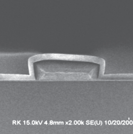
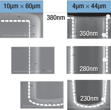
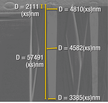
In the past year, considerable progress has been made in optimizing results for each of the unit processes involved (Figs. 1-5). In etch, optimization between etch rate, profile and related parameters are well understood, with excellent performance demonstrated on aspect ratios typically ranging from 4:1 to 12:1. A process for dielectric liner deposition has demonstrated >60% step coverage on aspect ratios up to 12:1. The capability for depositing in excess of 1µm of oxide on via sidewalls makes this a versatile film for a wide range of aspect ratios. Titanium or tantalum barriers and PVD copper seed layers have been co-optimized with electro-chemical deposition to ensure void-free metal fill. For via-last processes, thermal budget becomes a significant concern, since device wafers are processed while being temporarily bonded to carriers. Dielectric and PVD depositions have been refined to achieve desired mechanical and electrical film qualities and process performance at temperatures below 200°C.
Click to Enlarge
Figure 2. The CVD-based dielectric is capable of depositing conformal liners in a wide thickness range and enables electrically robust dielectric insulation for interposers and high-aspect ratio TSVs.

Depending on the TSV processing sequence adopted, dielectrics (oxide, nitride) or metal (copper, barrier) must be removed using chemical-mechanical polishing (CMP). Recent work has enabled optimal bulk removal rates with the requisite process controls to accurately transition between layers and preserve surface topography. Other advances have also improved the cost-efficiency of this step, contributing to the goal of optimizing the overall cost of the manufacturing sequence.
Click to Enlarge
Figure 3. Electrochemical deposition of copper can achieve a conformal lining and void-free fill for vias. A co-optimized etch, liner, and PVD barrier/seed ensure a broad fill process window.

The process steps outlined above (etch through CMP) have been developed primarily on production-proven 300mm platforms. Thus, the traditional risks associated with new equipment have been largely mitigated. Foundries and independent device manufacturers were able to start development work in 2008, with minimal new investment (hence, at low cost) by re-using existing equipment. Thus, it may be surmised that these processes can be ramped to pilot production as needed by the market, with full production capability later in 2011. Costs [inputs to the cost of ownership (CoO) model] are well understood in the industry, and CoO reduction roadmaps are easily comprehensible.

Click to Enlarge
Figure 4. Rapid removal of copper layers with good surface topography and end points at copper/barrier and barrier/oxide interface; co-optimized with electrochemical deposition for low cost of ownership.


Click to Enlarge
Figure 5. Redistribution layer relocates via locations. In TSV integration, it enables pads to be aligned between heterogeneous die. Shown is a copper redistribution line formed with PVD barrier/seed and electrochemical deposition, encased with low-temperature (<200°C) dielectric.

Bonding/debonding

The situation is different for temporary bonding and de-bonding of wafer carriers. While the learning from 200mm CMOS image sensors had been initially leveraged for preliminary 300mm silicon processing, several elements needed to be modified. Glass carriers are mandatory (for optical transparency) and remain in place as part of the image sensor end-product. Glass and silicon substrates have displayed the requisite mechanical handling repeatability. In high volume silicon processing for logic and memory (the focus of this article), carriers need to be re-used. Current lithography systems used in packaging fabs provide the alignment capability to look through silicon. Hence, glass carriers are not an absolute requirement. Silicon carriers are preferred as they are manufactured to industry- standard dimensional specifications, are less prone to breakage (and therefore easier to recycle), and can thermally and electrically couple with the wafer. In carrier management, the challenges are bonding tolerances, total thickness of the wafers and substrate, flatness of the substrate surface, thickness and thickness uniformity of the adhesive, adhesive coating, and processing and grinding. In the past two years, good progress has been made on developing appropriate adhesives, with second-generation bonding materials showing much improved results.

From a supply chain perspective, processed wafers need to be shipped between the TSV facility and outsourced assembly and testing, which can be done either as bonded wafers or on tape. For the former approach, bonding and de-bonding needs to be matched in terms of equipment set and put a constraint on the supply chain between the fab and the assembly house. Shipping on tape may be an acceptable option, but needs to be validated by the supply chain. It would behoove the industry to standardize on carriers, adhesives, and the associated processes of bonding and de-bonding so that these specific unit processes can be exercised in iron-man type testing and transitioned to cost-effective production. To drive this "standardization," the current collaborations between material and equipment suppliers and users need to be accelerated to release a commercial solution for temporary carrier management.

Conclusion

Today, unit processes are ready and integration is well advanced, with "best known methods" for typical interposer, via middle, and via last flows ready for limited pilot production at several locations. Products for TSV creation have been proven in the 300mm manufacturing environment and paths for process improvement and CoO reduction are well understood. Processes and products in wafer-level thinning and die-level processing are evolving rapidly.

For volume production, end-product value must be balanced against wafer cost. The end-product value will vary widely depending on application and hence the cost-threshold may vary. The total cost to achieve a device stack is split between wafer-level TSV creation (etch, dielectric liner, barrier/seed, ECD fill, and CMP), wafer-level thinning (bonding, thinning, and de-bonding) and die-level processing (dicing, stacking, assembly, and testing). Current costs of the latter two steps are in excess of 50% of the overall cost and industry standardization (or at least convergence) will help reduce the cost of materials and accelerate the release of higher throughput equipment.

Biography

Sesh Ramaswami is Sr. Director, Strategy in the Silicon Systems Group at Applied Materials; email  [email protected].

More Solid State Technology Current Issue Articles
More Solid State Technology Archives Issue Articles

Executive Overview

The motivation for developing higher density electronic packaging continues to be the market, primarily the high-volume cellular phone market. The consumer, after all, is expecting that each new generation of products furnish greater functionality, be smaller than its predecessor’s, provide higher performance and more memory for applications and data storage. There are two directions a company may choose when planning their product; expanded silicon integration (system-on-chip) or joining a number of existing silicon elements in a single package format (system-in-package). With volume manufacturing, product costs can be stabilized so that advanced IC package innovations become more available, even for other product segments.

Vern Solberg, STC-Madison, Madison, WI USA

The increase in electronic functionality can be achieved through the development of more complex silicon integration but that route generally requires a great deal of capital resources and time. A leading semiconductor packaging company executive stated, "In general, functions that can economically be integrated should be integrated using system-on-chip." The key word is "economically," and this puts constraints on the suitable application for the SoC package. Although the system-on-chip (SoC) approach can reduce system size and increased functional performance, the complexity of the design process and sorting out access to intellectual property (IP) controlled by others can be costly. Even more significant, development cycle time for the custom silicon product may be several months to several years, likely causing conflict with the life cycles for most cell phone products.

Click to Enlarge
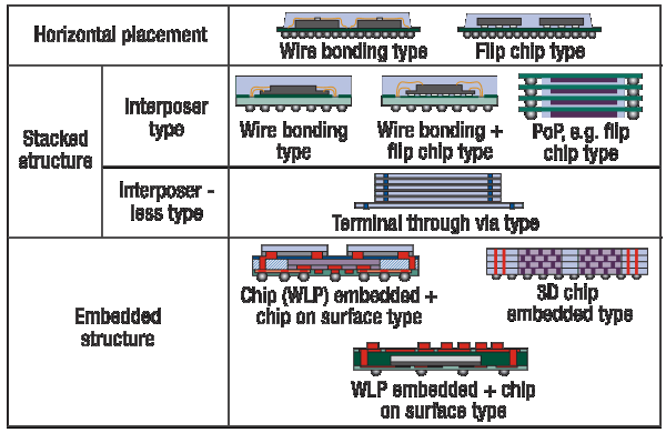
Figure 1. Variations of current system-in-package methodologies. SOURCE: iNEMI 2009 Industry Roadmap

To address the need for greater functionality quickly, a number of companies have already shifted away from single-die packaging and have adapted various forms of multiple-die system-in-package (SiP) innovations typical of those illustrated in Fig. 1. A market report prepared by Prismark identifies four categories of SiP:

Modules: including LTCC and PCB (printed circuit board)-based modules that combine one or more uncased die and integrated and/or discrete passive components in a ball grid array (BGA), land grid array (LGA), or castellated joint package. The majority of high volume module designs are for RF applications, such as mobile phone power amplifier modules and Bluetooth modules.

Multi-chip modules (MCMs): with multiple uncased die and optional passives in side-by-side and stacked die configurations with standard package outlines. Examples include graphics processor and memory MCMs as well as CPU and memory MCMs.

3D stacked-die packages: including any standard package outline with two to five (or more) vertically stacked devices with a lead-frame, PCB, or flex circuit base. The primary application is memory for mobile phones.

3D stacked package-on-package (PoP) and stacked package-in-package (PiP): PoP includes pre-packaged devices that are stacked on top of each other using lead-frame, PCB, and flex-based solutions. PiP includes stacked package configurations where one of the die stacks includes an over-molded package.

The first challenge for the package designer is to select the optimal SiP structure. For 2D applications, each die can be placed on the SiP interposer with either face-up (wire-bond) or face-down (flip-chip, stud-bump, or lead-bond). The module and MCM configurations are typically classified as a 2D structure and generally relies on ceramic, organic laminate or silicon as a base substrate to interconnect both incased and uncased devices. It has become more common for companies to use smaller passives and flip-chip mounting to reduce module size. In addition, many commercial component outlines have significantly decreased in size and advances in substrate manufacturing methodologies have enabled closer spacing between devices. A combination of high-density build-up fabrication technology along with the use of embedded passives can yield a very efficient 2D assembly as well.

The 2D package form factor, although ideally suitable for a wide number of applications, may not meet the small outline requirements demanded by wireless handset developers. Companies developing products for long-term high-volume application are adapting packaging methods that combine a number of functions within the confines of a single package outline. Stacking multiple die elements and/or joining individual package sections in a vertical configuration has proved to be a very efficient and economical format for minimizing package outlines. The multiple-die package is often proving superior to the system-on-chip alternative because it can economically integrate several different but complementary functions. The design of the 3D multiple die package, however, requires a clear understanding of the relationship between devices, the on-package interconnect requirements and ultimately, the interface between package and the interposer structure.

The benefit to the user is increased functionality in a smaller space, often two or three die are encased in a single, fine-pitch ball grid array (FBGA) package outline. The most efficient die-stack package assembly process utilizes die combinations with size variation that can be mounted sequentially in a pyramid fashion. When the same size die are stacked, the die must be individually mounted and wire-bonded before adding the next die in the stack. To clear the wire-bond loop on the lower die, a spacer must be provided between active die layers. The die-stack process allows the supplier to rapidly develop basic multiple-die combinations. Using the co-design methodology, supplier and user engineers can develop a product in a matter of weeks and optimize the overall system interconnect to minimize or eliminate package design re-spins that saves both hardware costs and design cycles.

Direct joining of bare die has evolved as viable process for same size die using through-silicon-vias (TSVs) to join one silicon layer to another. The process, most commonly employed for memory applications, enables the joining of several layers of very thin die elements into a single monolithic form factor. There are, however, significant drawbacks to die-stacking. Unless all of the unpackaged bare die are pre-tested and known to be good (KGD) before assembly, the multiple-die package yields may be well below the acceptable levels traditionally established for the single-die package.

Package stacking reduces risk

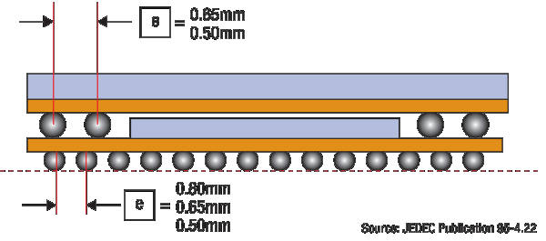
The package-on-package (PoP) innovations are proving to be far more predictable for a broad range of SiP applications. User companies have realized that complex mixed-technology functions can be produced with higher yield and more economically if the semiconductors are individually pre-packaged and tested before joining. The most common solution for PoP applications utilizes package sections designed around the JEDEC standard array packaging format (Fig. 2). Stacking pre-packaged die has less risk because the individual packages are fully tested before conversion to the stacked PoP format.

Click to Enlarge
Figure 2. JEDEC Standard format for package-on-package components. SOURCE: JEDEC Publication 95-4.22

Acknowledgment

Bluetooth is a registered trademark of the Bluetooth Special Interest Group.

References:

  1. Prismark Report, 2009 SiP Roadmap.
  2. 2009 iNEMI Industry Roadmap, Component and Subsystem Technologies Section.
  3. IPC International Technology Roadmap for Electronics, 2008-2009, Part B, Technology Trends and Part D, Component Packaging.
  4. ITRS White Paper 19.0, The next Step in Assembly and Packaging: System Level Integration in the package (SiP).
  5. Yole Développement, 2009 Report, Memory Applications: Packaging and Integration Trends.

Biography

Vern Solberg is an independent technical consultant based in Madison, Wisconsin specializing in design and assembly process implementation for surface mount and microelectronic technologies;email  [email protected].

More Solid State Technology Current Issue Articles
More Solid State Technology Archives Issue Articles

(July 30, 2010) — Package on package (PoP) stacking makes use of the vertical space available on electronics printed circuit boards (PCBs). It increases density, fitting more silicon into the same footprint. However, package stacking can be difficult, as fine pitches require placement accuracy, and taller stacks generally face reliability issues, especially if the stack is reflowed improperly. So where should PoP stacking take place?

Take this short survey and tell us what you think, and why: http://www.surveymonkey.com/s/packageonpackage

Read about other 3D packaging technologies and read Advanced Packaging’s online feature about PoP rework from BEST Inc.

(July 30, 2010) — In this video interview, Craig Mitchell, Tessera, comments on 3D packaging and interconnect, speaking with senior technical editor Debra Vogler. The chip industry is using packaging technologies to address miniaturization and density. Materials are posing a challenge.

Mitchell sees copper taking a more important role with better cost and reliability. Flip chips are migrating to finer geometries, and low-k dielectrics are very fragile, prompting a change in interconnect and passivation technologies.

Mitchell also explains Tessera’s recent Cu development, wherein Tessera is working in copper application from substrate up to the die. This minimizes changes to the die side, making use of substrate technology instead.

See more packaging articles and news here: http://www.electroiq.com/index/packaging.html

(July 28, 2010) — In this video interview, Philip Garrou, microelectronics consultant and Advanced Packaging blogger, offers information on his blog, Insights from the leading edge, and summarizes reasonable roadmaps for 3D technology and TSV in particular. 2012 mainstream adoption seems too aggressive to Garrou.

Read Garrou’s blog, Insights from the Leading Edge

Recent post:

CMP, CMC and MOSIS have announced a multiproject wafer run for Jan 2011. MOSIS has been known for years as a supplier of prototype IC runs …

>> Read the Blog

by James Montgomery, news editor

July 26, 2010 – There was a great deal of buzz at SEMICON West about 3D ICs, thanks to down-the-street ASMC presentations and backend discussions and vendors present. Through-silicon vias (TSVs) in particular are a hot ticket — so much so that traditional frontend equipment suppliers are touting their entry. (Novellus, for example, made a splash with a suite of tools for wafer-level packaging dubbed "The New Vertical Reality," staking claim to what it says is a $700M+ market.)

(Phil Garrou also summed up several 3D/TSV presentations from SEMICON West: the TechXspot session on "Bridging the Gap," and Suss Microtec’s "3D IC Bonding and Thinned Wafer Handling Workshop.")

There are more than 15 300mm 3D IC pilot lines now, according to SEMI’s Jonathan Davis, priming the Tuesday Executive Panel’s discussion about 3D ICs. Lam’s Steve Newberry predicted the industry will see widespread adoption in 4-5 years (maybe 2-3), though standards are needed to more efficiently implement it — e.g. will it be via-first, via-last, something else? It’s also a relatively small market (a "niche" for etch, in LRCX’s view), so ROI will be tough to justify for some, and few players will be able to pay for the R&D. AMAT’s Thakur takes a broader view of 3D IC opportunities, emphasizing formfactors and performance. GlobalFoundries’ Tom Sonderman likened TSV adoption to that projected for EUV lithography, requiring collaboration and a need to identify value-adds.

More "lessons learned" from SEMICON West 2010:
Lesson #1: Good times here, for now
Lesson #2: Capital intensity & EUV
Lesson #4: Supply chain challenges
Lesson #5: Interests outside CMOS

3D and TSV offer attractive growth, but there are still questions and hype to resolve. "While front-end semicap companies were very bullish on TSV, some back-end contacts wondered aloud how TSV will reach meaningful volumes soon as some critical standards are still not formulated," writes Credit Suisse’s Satya Kumar. Citing the challenge of getting market penetration with "more capable, but also more expensive tool sets, to an end market that has traditionally used low-end, very low-cost tools," Deutsche Bank’s Steve O’Rourke projects adoption of TSVs will start in traditional wafer fabs first, then "potentially" move to backend fabs, with prices lower — "but not by much" than traditional frontend tools. Winning strategies will present "a combination of capabilities and cost of ownership arguments," he writes — but "we maintain healthy skepticism on timing and market size expectations."

Though efficiency can offer a valuable proposition, it’s hard to overstate how hugely important are costs (low) and availability (now) to backend customers. Several people with whom we talked at SEMICON West about how traditionally more frontend-oriented tool suppliers are clamoring for growth in packaging suggested it might be a tough sell, especially at the subcon level. One industry watcher said that OSATs have a simple interface point for these folks: ask them about lead-times, and if the answer is anything more than three weeks the conversation’s abruptly over. Another pointed out that in many cases, backend outsourced firms translate "lead-time" as the time it takes to walk to the dock, unwrap the plastic from one of a long bank of tools already sitting around, and plug it in.

TI’s Cu pillars

Packaging wasn’t just a hot topic among suppliers. Texas Instruments made a splash with partner Amkor, announcing qualification and production of a fine-pitch Cu pillar flip-chip package — <50μm, vs. ~150μm pitch size limitations with conventional solder-based flip chip, e.g. ball bond.

Cu pillars offer advantages over conventional solder in terms of thermal performance, better conductivity, and resistance to electromigration, as well as shorter package routing (higher pin densities, reduced die sizes). The industry is investigating their use for various reasons, e.g. as an alternative to wafer-level packages for analog devices, or replacing gold wire in some packages. Intel uses Cu pillars in its 65nm and 45nm flip-chip products (and is expected to continue through 32nm).

TI executives explained the technology is ideal for applications ranging from ASSPs (smaller body size, high pin count, low-power aspects) to DSPs (same requirements), and power management (density more than pin count) — and they’ve got customers already lined up in all three product areas. "We looked at least two other alternatives" besides Cu pillars, and "we actually built products on them, they worked fine," noted Devan Iyer, TI’s manager of worldwide semiconductor packaging. "But on the long-term roadmap, we feel like Cu pillar is the most cost-effective, the most standard in the industry."

The TI/Amkor announcement "represents one of the major adoptions outside of Intel and I believe it is the start of the wave," Jan Vardaman, president/founder of TechSearch, told SST, in conversations during and after SEMICON West. She added that she sought out the first major product known to employ the Cu pillars, a hot-selling smartphone (whose backer rhymes with "Frugal") — but found it to be sold out in the wireless provider’s store, despite a stated retail price north of $600 (without a contract).

(July 23, 2010) — In these three video interviews from SEMICON West 2010, Leti research directors speak with senior technical editor Debra Vogler. Yannick Le Tiec discusses cleaning; Michel Brillouet speaks on 3D packaging work, and Didier Louis updates us on advanced lithography.

In "Leti Advanced Lithography Program update," Didier Louis, International Communication Project Leader at Leti, summarizes the status of lithography development at the organization. Leti is pursuing two alternatives to “waiting for EUV:” maskless, multi-beam lithography and dry, 193nm lithography with double-patterning and a spacer. Louis reports that 15nm resolution has been attained for isolated lines. Didier also presented at the lithography breakfast at SEMICON.

In "Leti cleaning methodology update," Yannick Le Tiec, Leti’s assignee to IBM, talks about developing new protocols for cleaning at 32nm and below. They are targeting low-power applications, and find some better than others.

Finally, in "Leti update on 3D packaging," Michel Brillouet brings us up-to-date on Leti’s 3D packaging tech: wafer thinning and bonding, and the associated handling concerns. Integration for wireless applications is Leti’s current interest. Partnerships enable better package design. Read more about advanced packaging here.

(July 23, 2010) — In this video interview shot at SEMICON West 2010, Mark Privett, Brewer Science, says that new technologies allow use of higher temperatures as well as room-temperature processes, such as wafer de-bonding. The 3D packaging industry is nearly ready for high-volume, yet still without industry standards.

To see the company’s earlier 2010 interview, recorded at the ConFab with CTO Tony Flaim, click here: http://www.electroiq.com/index/display/semiconductors-article-display/2383506614/articles/solid-state-technology/semiconductors/industry-news/business-news/2010/may/confab-video__end.html