Category Archives: 3D Integration

July 13, 2011 — Stanley T. Myers will retire as SEMI president and CEO later this year. At SEMICON West 2011, he tells Debra Vogler, senior technical editor, what moments stand out for him as "historic" advances in semiconductor fab and the evolution of SEMI. He also shares advice for young engineers entering the semiconductor industry.

In the early days, silicon engineers were finally able to make floats on crystal 1" in diameter. This led to the development of the 0 dislocation crystal, Myers says, which in turn prompted the semiconductor industry’s scale-up from 200 to 300mm wafers. The chip industry advances in this way, Myers notes, with one breakthrough building on another.

3D IC and through silicon vias (TSV) are fascinating technologies that will propel the continuation of Moore’s Law, Myers adds, looking to the semiconductor manufacturing industry’s future.

At SEMI, he considers most important the organization’s ability to bring together all members on global action items that matter to the semiconductor and adjacent markets. It was a historic moment for SEMI when the association created regional presidents and boards to focus on issues important to specific geographies, said Myers.

Advice for young engineers? "You’re going to do things and you’re going to fail…Fail well, fail fast, and move on," Myers advises, saying that this mindset allows you to accomplish anything. 

Subscribe to Solid State Technology/Advanced Packaging

July 11, 2011 — This week at SEMICON West in San Francisco, imec is demonstrating a viable implant-free quantum-well (IF-QW) pFETs with an embedded silicon-germanium (SiGe) source/drain and 3D integration of a commercial DRAM chip on top of a logic IC.

Imec SiGe IF-QW pFET a "viable option" for 16nm node

Imec has fabricated implant-free quantum-well (IF-QW) pFETs with an embedded silicon-germanium (SiGe) source/drain. Short channel control and logic performance results are strong, benchmarked against competing technologies (SOI nFET, SiGe-FET). Drain-induced barrier lowering is ~110mV/V at 35nm-LG and 1mA/

July 6, 2011 – EV Group has joined Georgia Tech’s 3D Systems Packaging Research Center (PRC) as a "manufacturing infrastructure member." Specifically, EVG will contribute its know-how and technology in temporary bonding and debonding, chip-to-wafer bonding and lithography technology, and associated product and processes to the PRC’s Silicon and Glass Interposer Industry (SiGI) Consortium research program.

Launched earlier this spring, the SiGi Consortium is pursuing development of less expensive (up to 10

July 5, 2011 – On June 27th Elpida Memory announced that it had begun sample shipments of DDR3 SDRAM (x32-bit I/O configuration) made using through-silicon via (TSV) stacking technology. The device, according to the company, is a "low-power 8Gb DDR3 SDRAM that consists of four 2Gb DDR3 SDRAMs fitted to a single interface chip using TSV."

Target applications reportedly include tablet PCs, extremely thin PCs, and other mobile computing systems. The new TSV DRAM will reportedly enable significant energy savings as well as making portable electronic devices smaller, thinner and lighter. Elpida believes that the new devices in notebook PCs will demonstrate a 20% reduction in operating power and a 50% reduction in standby power compared with systems that use the standard SO-DIMM configuration which use standard wire bonding technology. Power consumption is reduced because the TSVs shorten the interconnect between the chips, thus reducing parasitic resistance and capacitance.

In addition, chip height is decreased and the DIMM socket is eliminated. Chip mounting area is reportedly reduced 70%.

Exactly one year ago, Elpida Memory, Powertech Technology (PTI), and United Microelectronics Corporation (UMC) announced a three-way 3D IC partnership to leverage the strengths of Elpida’s DRAM, PTI’s assembly, and UMC’s foundry logic technologies to develop a total 3D IC Logic + DRAM integration solution. That partnership was finalized last month.

Elpida began developing TSV technology in 2004 on a Japanese grant from NEDO (the New Energy and Industrial Technology Development Organization). In 2009 it demonstrated the industry’s first TSV DRAM based on stacking together eight 1GB DDR3 SDRAMs.

by Hughes Metras, U.S. development, Leti

June 28, 2011 – Leti CEO Laurent Malier opened CEA-Leti’s 13th Annual Review in Grenoble, France, on Monday by noting the important role that research and technology organizations (RTOs) should play in strengthening industry in Europe. Unlike other regions (such as the US) where applied R&D depends mostly on individual companies and industry alliances, Europe counts several of such organizations — including Leti, Liten, Fraunhofer Mikroelektronik, CSEM, VTT, TNO, imec, and Sintef — which are assets for industry that support innovation through private/public partnerships.

Beyond continuing investment in CMOS technology and lithography, Leti has taken a leading position in 3D technology. After having transferred the first technology in production in 2009, Leti has opened a full 300mm prototyping line capable of running all key process steps from wafer bonding to elaborations of interconnections.

Over the past two years, Leti has built strategic R&D partnerships with most of France’s chipmakers to help them meet an increasingly competitive global business and technology environment. Similarly, this model of technology platform and pilot lines is proposed by the High-level Group for Key Enabling Technologies launched in 2010 by the European Commission.

Malier explained the valuable link between nanotechnologies and applications, which has allowed Leti to launch 40 startups over the past 20 years, as well as to explore an innovative path in sectors such as medicine and healthcare. He noted a new initiative created in 2010 to accelerate innovation in medicine — Clinatec, which will open this year, will gather physicians, biologists, and technologists to develop healing protocols for brain and nerve diseases.

by Michael A. Fury, Techcet Group

June 20, 2011 – Seventy attendees comprised the standing room only crowd at SEMI’s HQ for the special June 15 NCCAVS user group meeting on 3D Packaging, co-hosted by three of the Bay Area User Groups: CMP, Plasma Applications, and Thin Film. The presentations will be posted on one or more of these groups at http://www.avsusergroups.org/ as soon as they are available.
Rob Rhoades, CTO of Entrepix, led off the session with a review of CMP issues unique to through-silicon vias (TSV). Copper is the prevalent choice for TSV metal fill, being used 2

June 16, 2011 — Mentor Graphics Corporation (NASDAQ:MENT), in a cooperative effort with Tezzaron Semiconductor and MOSIS, created a process for economically developing and manufacturing 3D-IC prototypes on multi-project wafers (MPWs). The process enables designs using tens of millions of through silicon vias (TSVs) with dimensions as small as 1.2 x 6µm and 2.4µm pitch, producing up to 300,000 vertical interconnects per mm2.

MOSIS’s Multi Project Wafer (MPW) services now allow users, via Tezzaron, to test out 3D-IC concepts using the same provider and model they currently use for their standard semiconductors, said Wes Hansford, director at MOSIS, who added that resource and schedule coordination reduces the "effort and risk" in moving silicon roadmaps forward. MOSIS manages MPW projects including reticle creation, fab reservations, final packaging and testing, and other logistics.

Tezzaron enhances customer designs as required for successful 3D-IC integration and also provides backend manufacturing steps including wafer thinning, backside metal and wafer bonding.

Mentor Graphics provides DRC and LVS tools that support 3D-IC physical verification, ensuring that designs are correct and will meet 3D process requirements. Mentor Graphics brings production-certified Calibre solutions to the prototyping step, verifying that "3D-IC designs are manufacturable," said Joseph Sawicki, VP and GM of the Design-to-Silicon Division at Mentor Graphics. "The Calibre solution uses foundry-certified PDKs from MOSIS wafer suppliers with extensions for MOSIS-Tezzaron 3D-IC designs."

Customers can use the 3D-IC service to create proof-of-concept ICs that demonstrate the use of high-density TSVs in stacked die configurations for intelligent sensor, multi-core processor and many other applications. 

MOSIS is a low-cost prototyping and small-volume production service for VLSI circuit development. For more information about the 3D-IC prototyping service, visit www.mosis.com.

Tezzaron Semiconductor specializes in 3D wafer stacking, TSV processes, and cutting-edge memory products. Learn more at www.tezzaron.com

Mentor Graphics Corporation (NASDAQ:MENT) provides electronic hardware and software design solutions. Learn more at http://www.mentor.com/.

Subscribe to Solid State Technology/Advanced Packaging.

Follow Advanced Packaging on Twitter.com by clicking www.twitter.com/advpackaging. Or join our Facebook group

By Debra Vogler, senior technical editor

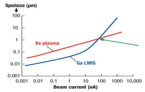
June 13, 2011 — FEI launched its Vion plasma focused ion beam (PFIB) system based on inductively-coupled plasma (ICP) source technology using a xenon ion beam. The system generates more than a micro-amp of beam current and can remove material faster (>20× improvements in speed, Fig. 1) than liquid metal ion sources that typically max out at a few tens of nano-amps, according to the company. Because of its speed, FEI will target new technologies, such as 3D packaging and 3D transistor design technologies, where PFIB analysis is more practical.

Click to Enlarge
  • High-volume milling/high beam current
  • Ga-FIB loses size advantage to plasma source as beam current goes above 50-60 nA
  • Xe has high sputter yield, high brightness, and low energy spread
  • No Ga contamination

Figure 1. Plasma FIB is 20× faster than current FIBs. Its fast ion milling capabilities enable rapid cross-sectioning of features from 50-1000µms. SOURCE: FEI

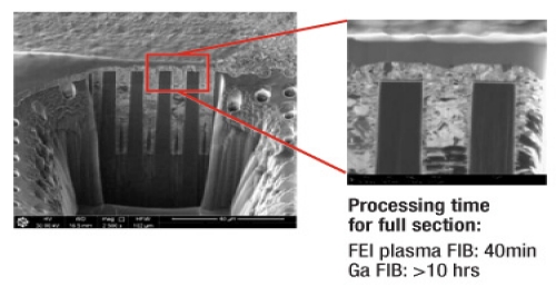
In a podcast interview, FEI product marketing manager Peter Carleson explained that gallium FIBs are already used for packaging applications, but with the cross-sections and trenches necessary for such applications (in the neighborhood of ~100µms), the removal process can take three, four, or even 8 hours. With the new source’s higher beam current, more samples can be done with greater tool utilization. The PFIB can also access lower regions of stacked dies to do traditional failure analysis or debugging (with the device "on") on the devices in the lower regions. The PFIB also enables quicker cross-sectioning of 3D integrated circuits that use TSVs/interposer layers (Fig. 2).

Click to Enlarge

Figure 2. High-speed sectioning of TSVs with plasma FIB. The device was located, cross-sectioned, polished, and imaged with PFIB. SOURCE: FEI

The product can perform site-specific removal of package and other materials to enable failure analysis and fault isolation on buried die; and circuit and package modifications to test design changes without repeating the fabrication process or creating new masks. Other applications include process monitoring and development at the package level, and defect analysis of packaged parts and MEMS devices.

Listen to the podcast:


  • Format: mp3
  • Length: 4:29
  • Size: 4.10 MB
  • Date: 06/13/11