Category Archives: 3D Integration

by Dr. Phil Garrou, contributing editor

January 7, 2010 – On December 6th, Ziptronix Inc. filed a complaint of patent infringement against Omnivision Technologies, TSMC Ltd and TSMC North America in US District court, alleging that the defendants "willfully and deliberately infringed" on several patents pertaining to low-temperature oxide bonding.

Omnivision acknowledged the patent infringement complaint in its recent 10Q filing with the Securities and Exchange commission, and responded that they plan to "vigorously defend ourselves" against the allegations.

When asked for comment, Ziptronix CEO Dan Donabedian referred to the company’s "extensive patent portfolio" that enables manufacturing of backside illumination CMOS image sensors. "Ziptronix respects the intellectual property of others and expects others to do the same," he said, and pledged that the company "will vigorously monitor all acts of infringement and take the necessary actions to protect its intellectual property and the interests of its duly authorized licensees."

Founded in October 2000, Ziptronix was spun out from North Carolina’s RTI International for the purpose of commercializing wafer and die bonding technology. In the intervening years, such technologies have found an important role in the evolving areas of chip-on-chip (CoC) bonding, 3D IC integration, and CMOS image sensing.

Ziptronix’s patent portfolio is centered around its ZiBond (Ziptronix bonding) and DBI (direct bond interconnect) technologies. ZiBond is based on their discovery that one can achieve significantly higher bond energy between wafers (with thermal or other oxide) after treatment with various surface "activating and terminating" processes. The direct oxide bonding, which is initiated at low temperature, is characterized by a very high bond energy between the surfaces.

In 2008, Donabedian offered a warning that "the broad and fundamental nature of our patent portfolio leads us to believe that any use of a oxide low-temperature bonding process is highly likely to be covered by one or more of our patents."[1]. While acknowledging the availability of some commercial tools that claim to support low-temperature oxide bonding processes, the company had neither granted nor intended to grant any IP licenses to equipment manufacturers. "Anyone running a low-temperature oxide bonding process as part of their manufacturing scheme is likely to be infringing on our IP," he said.[2] In Nov. 2009 Raytheon Vision Systems reached a licensing agreement for the use of Ziptronix’ DBI technology in Raytheon’s imaging systems.


[1] "3D Startup Proves Ahead of Its Time", Semiconductor International, Oct. 2008
[2] "Ziptronix Pioneering 3D Integrated Circuit Process Technology", i-Micronews, Aug. 2008

by Dr. Phil Garrou, contributing editor

January 6, 2010 – At the RTI 3-D Architectures for Semiconductor Integration and Packaging Conference in Burlingame CA, fresh off the 3D announcements of IBM and Samsung, several industry leaders focused on the imminent use of 3D interposers.

Arif Rahman, principle engineer at Xilinx, gave further details on their next-generation FPGA products that have been reported recently. When asked about their choice of a silicon interposer for their next-generation FPGA, he noted that "it appeared to be the most manufacturable way to offer product performance during our required timeline." The interconnect on the interposer is done at 65nm technology.

Douglas Yu, senior director of interconnect and packaging at TSMC, was likewise questioned about the foundry’s commercial commitment to silicon interposers (Xilinx is their customer), and he confirmed that TSMC will offer commercial silicon interposers.

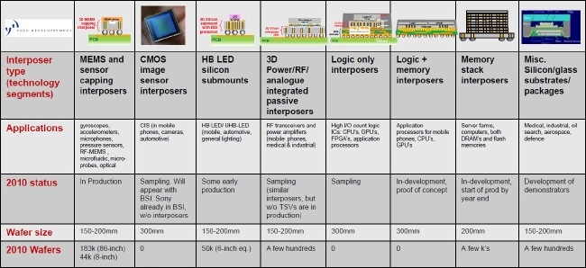
Jean-Marc Yannou , senior analyst at Yole Développment, pointed out that that silicon/glass interposers offer >10× more resolution and finer pitches than traditional organic substrates. Yole has identified eight categories of applications for silicon/glass interposers: MEMS; CMOS image sensors; LED submounts; RF with passives; logic; memory + logic; memory stacks; and miscellaneous.

Click to Enlarge
2010 status of 3D silicon/glass interposers.

Songdong Cho, senior engineer in Samsung’s system LSI group, noted that mobile products will require more than 25GB/sec bandwidth and therefore "wide I/O memory with TSV appear to be the only solution." He described two platforms within the systems LSI group: Interposer and memory on logic.

Tzu Kun Ku, director of ITRI — which was on track to have its 300mm line baseline process completed by year’s end 2010 — described how interposers will reportedly reduce both system form factor and bill of materials simultaneously.

Click to Enlarge


Leti on more Moore for TSV


January 3, 2011

(January 3, 2011) — The semiconductor industry’s ongoing discussion of "more Moore" and "more than Moore" at IEDM 2010 (12/6-12/8/10, San Francisco, CA) was continued with another invited paper presented by Leti researchers (paper #2.6, "Engineered substrates and 3D integration technology based on direct bonding for future More Moore and More than Moore integrated devices"). Laurent Clavelier, head of solar technologies department at Leti, discussed the significance of the paper with Debra Vogler, senior technical editor.

Listen to the podcast interview:  Download (for iPhone/iPod users) or Play Now

According to Clavelier, the researchers used both Smart Cut and Smart Stacking technologies in their work. In the "more Moore" domain, the applications include SOI substrates as well as strained SOI, and the introduction of special layers, such as diamond. For one application, the group combined Smart Cut technology with 3D integration to create functions not feasible with monolithic integration.

Click to Enlarge
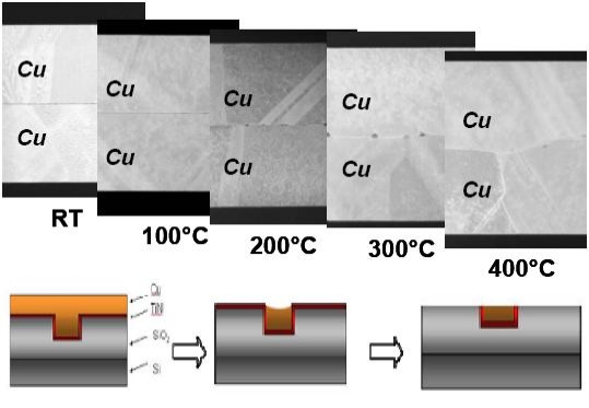
Figure 1. Schematics of the CMP process (top) used for Cu/Cu direct bonding and TEM analyses (bottom) of the bonding interface as a function of temperature. SOURCE: Leti 

To evaluate such 3D integration, the group used a room temperature and atmospheric pressure direct Cu/Cu bonding that is fully compatible with classical copper back end of line (BEOL) and TSV silicon process (Figure). The paper noted that the polishing steps were customized.

Continue reading about this paper in "Leti on more than Moore for RF filters" in the ElectroIQ Semiconductors Center 

by Dr. Phil Garrou, contributing editor

December 22, 2010 – Global 3D IC technology leaders recently assembled in Munich at the IEEE 3DIC Conference in Munich, with Peter Ramm (Fraunhofer EMFT Munich) and Eric Beyne (IMEC) as co-chairs.

Jeff Burns, director of VLSI systems at IBM/Yorktown Heights, offered the perspective that 3D IC technology "will require many changes to architecture, VLSI design, design IP, tools, technology, and manufacturing." In total, this promises to be much larger in scope than a CMOS technology generation — rather, "it will be similar to the transition from bipolar to CMOS," he said.

Ionut Radu, director of direct bonding technology at Soitec, revealed that standard damascene copper CMP does not provide the desired surface topography needed for a successful copper-copper bonding process due to Cu pad dishing and oxide erosion. Cu-Cu direct bonding, performed at room temperature under atmospheric pressure, requires flat surfaces with <1nm surface micro-roughness. Radu indicated development of a proprietary CMP process to limit the surface topography between the copper pads and the surrounding oxide dielectric. The special CMP surface preparation step leads to micro-roughness of both Cu and dielectric surfaces beings as low as 4-5Å.

Bonding of 5μm Cu pads has been successfully performed with a corresponding bonding energy of more than 1J/m2 obtained upon 200°C post bond anneal. The achieved bonding strength is reportedly sufficient to sustain post-processes such as silicon back thinning using coarse and fine grinding. Since no external force or pressure and temperature cycle is applied during bonding process, excellent alignment with minimum mechanical deformation is obtained.

Kiyoto Ito, researcher at Japan’s ASET (Association of Super-Advanced Electronic Technologies) described two 3D interconnection architectures — block and sandwich stacking — for stacked processor-memory LSIs. In the sandwich configuration, memory chips and processor chips are stacked alternately, and vertical interconnects in each PU-CHIP are divided into two groups: interconnects for global communications and interconnects for local 3D memory communications. Compared with block stacking configuration, sandwich stacking architecture shows 38% fewer vertical interconnects for the same throughput and reduces power consumption by 21%.

Dimitrios Velenis, design and cost expert at IMEC, discussed the impact of different manufacturing options on the cost of a 3D-stacked system. IMEC has developed a cost model based on its own 3D integration process flows to analyze and compare the cost effectiveness of different technology approaches.
When examining through-silicon via (TSV) processing cost vs. depth they find TSV depth affects the time for etching, liner and barrier deposition, and plating steps. TSV diameter and pitch affect the total area of a chip, the number of chips on a wafer — and eventually the cost of a 3D stack. Therefore, the cost of TSV processing increases with TSV depth and increasing aspect ratio.

Dean Malta, manager of Microfabrication Engineering at RTI International, shared his experiences on the fabrication of 3D TSV interposers by both TSV-first and TSV-last processes. In the backside TSV-last process, TSVs are formed after the front-side thin film processing is completed. Since these vias do not need to be filled, TSV reliability concerns due to Cu-Si CTE mismatch are reduced. Backside TSV processes must be compatible with the thermal limitations of the front-side thin film layers should they include polymer dielectrics.

The biggest challenge, Malta noted, occurs with making the interconnections between the TSVs and the front-side metal during bottom clear: "Too much etching can result in high TSV leakage currents, due to sidewall passivation loss, while too little etching can result in high resistance interfaces," he explained.

In the TSV-first process, the TSVs are etched as blind vias, from the front surface of the wafer. A significant advantage here is that the passivation "bottom clear" etch is not required as in the TSV last approach. Also, since there are no other materials on the wafer at the time the TSV are insulated and filled, high-temperature processes such as thermal oxidation can be used to produce high-quality oxide insulation. There is, however, concern over the copper-filled TSV CTE mismatch issues. Malta suggested a way to address these reliability concerns is to "limit the TSV diameter," but he added that for small-diameter TSVs "with an acceptable aspect ratio for processing, it may be necessary to thin the interposer wafer significantly." RTI studies were done with 100μm-diameter TSV with 6:1 AR, and TSV passivation was 2μm thermal oxide.

Malta also observed thermo-mechanical issues during backside BCB or PI RDL curing processes at temperatures of 250°C and 350°C, respectively. He believes the polymer delamination and cracking observed in the areas over the Cu-filled TSVs is due to copper protrusion during the dielectric cure. Separate tests at 400°C confirmed that the Cu in the TSV goes through a permanent expansion of 1.5-2μm during the 400°C exposure. In agreement with others in the industry, Malta found that these issues can be minimized by annealing Cu TSV at ~400°C after formation, and CMP of the resulting Cu protrusion.

by Dr. Phil Garrou, contributing editor

December 15, 2010 – With a general consensus that CMOS is becoming economically if not technically less and less viable as the industry continues to scale, it is to be expected that we will be seeing more and more 3D IC presentations at IEEE’s premier device conference, the IEDM (International Electronic Devices Meeting).

During his keynote presentation, Jim Clifford, SVP and operations GM at Qualcomm, indicated that scaling was becoming to expensive and therefore the company was backing 3D through-silicon via (TSV) technology. He urged the rest of the industry to "collaborate on 3D IC and invest in its infant infrastructure."

Conventional scaling has become more challenging in terms of materials, patterning and electrical performance, and now requires huge capital investments, noted Kinam Kim, president of Samsung Advanced Institute of Technology (SAIT), in his keynote presentation on the future of silicon technology. Current scaling strategy, he said, "is almost unusable for the 10nm node."

Kim expects mobile processors, FPGAs, and high-performance ASIC applications will require more functionality at greater speeds, which will necessitate "a heterogeneous device stack with a wide I/O interface and high data rates." 3D IC technology, he noted, is being adopted "as a promising solution for these devices."

In a presentation on 3D integration for the 28nm node and beyond, TSMC researchers indicated they have successfully integrated 3D technology into advanced CMOS foundry processes, described as "a major step toward 3D production."

Of special interest are the TSMC studies on Cu protrusion and its effects on device fabrication and reliability. As the system cools down from thermal excursions, mismatches in CTE between Si, SiO2 liner, and Cu introduces two un-desirable effects:

  • Cu extrusion around the center of the TSV. They find that protrusions depend on several process parameters, including the electroplating processes (ECP), electrolyte selection, impurities co-deposited with Cu, Cu grain size distribution, and post deposition annealing conditions.
  • Liner cracking. Having the smallest CTE, the oxide liner undergoes high stresses exerted by the Cu TSV and the Si substrate. The maximum stress concentration is found to be near TSV bottom, where the majority of liner cracks were observed that causes significant current leakage. TSMC has reportedly found solutions to these issues which strongly impact chip yield.


3D-induced stresses are one of the key constraints in a 3D design flow that must be controlled in order to preserve the integrity of front-end devices. IMEC and some of their consortium members (Panasonic, Qualcomm, Samsung) examined the stress induced by single- and arrayed TSVs, quantifying the stress distribution and determining its impact on both analog and digital FEOL devices and circuits. They conclude that stress aware design and accurate keep-out-zone (KOZ) dimensions will be needed to optimize silicon usage.

From stress modeling and experimental data, the IMEC consortium has developed transistor KOZ for both digital and analog circuits. The IMEC researchers conclude that the KOZ for a large matrix of TSVs is over 200μm for analog circuits and 20μm for digital circuits, and add that the complex interaction of stress components makes it difficult to use simple design rules without sacrificing large layout area. Depending on the TSV footprint and the number of TSV required, different TSV placements will be optimum (single, row, matrix).


Dr. Phil Garrou from Microelectronic Consultants of NC is a contributing editor for Solid State Technology and Advanced Packaging on www.ElectroIQ.com. Read his blog, Insights from the Leading Edge.

by Michael A. Fury, Techcet Group

December 15, 2010 – Following a morning of IEDM keynote talks, the IEEE held a press briefing to give the section chairs an opportunity to highlight what they felt were the most newsworthy talks in their sessions, some of which I chose to attend over the next two and a half days. I can say in retrospect that there was only a moderate correlation between these newsworthy recommendations and talks that were standing room only — the audience clearly knows its way around the dance floor.

During the press briefing, the question was raised about whether or not through-silicon vias (TSV) still qualify as an emerging technology. I thought the response was insightful: when reliability papers begin to appear on a topic, it is no longer an emerging technology. Congratulations, TSV; you are now of legal age. (Be smart, backfill responsibly!)

(Additional information can be found online at 2010 IEDM Technical Program. All figures are reproduced with permission of IEDM.)


5.1: My personal plunge back into device processing began with C.H. Lee of Samsung and a 27nm NAND flash memory with a reported record low 0.00375μm2 unit cell size. VTh distribution is reduced by 50% by using self-aligned reverse patterning in place of self-aligned double patterning, which reduces the bar CD from >10% to <5%. A novel B doping profile gives an initial VTh shift of 500mV with lower leakage. The three-level charge device has a lifetime spec of only 500 cycles, whereas the two-level device is spec’d at 1000-3000 cycles; they will be targeted to different markets.

Cross-section HRTEM images of the 27nm cell profiles. Active bar CD is 25nm.

5.2: Presenting to a standing-room-only-crowd, K. Prall at Micron showed joint work with Intel on a 25nm 64Gb MLC NAND with a cell size of 0.0034μm2, which includes 22% overhead. For perspective, the ±5% CD control corresponds to ±3 silicon lattice constants. The STI has a 7:1 AR, and an air gap reduced bit line interference by 25%. At these dimensions, the device uses 30-50 electrons to achieve the state change of 300-500mV. Channel conduction occurs in filaments corresponding to less boron doping; the doping is nominally random but boron clustering does occur.

Cross-section of the cell in the WL direction showing the WL airgap and reduction in total FG-FG coupling with airgap (red square) and without (blue diamond). WL bending is caused by sample preparation. A 25% reduction in total interference is achieved with the airgap.

2.3: The stress/strain characteristics of TSV & microbumps in thinned (~10μm) wafers were quantified by M. Murugesan of Tohoku University using μRaman spectroscopy, XPS and I-V curves. CMP was found to give a lower Ra and lower residual stress than ultra poly grinding (UPG), dry polishing (DP), wet etching or plasma etching (PE). CMP residuals were +10MPa to -30MPa, mainly tensile with a periodic distribution. UPG residuals were ~60MPa and DP were ~175MPa, all compressive, indicating that DP is not a suitable stress relief method.

2.4: A novel lock-and-key method for wafer-level 3D integration with tungsten TSVs was presented by K.N. Chen of National Chiao Tung University in collaboration with IBM Research. The lock-and-key structure limits misalignment compared to an oxide recess strategy. The joint resulting from the CuO-CuO bond (400°C for 1hr at 20mTorr under 10kN force) is seamless, with no residual interface visible by TEM. A seal ring around each chip periphery effectively prevents corrosion of the active chip bonds and provides additional mechanical strength to the system.

Left: Top wafer, Cu key structure, bottom wafer, Cu lock structure.
Right: (a) image of lock-and-key Cu bond structure integrating
2.7μm W TSVs in a 47μm thick Si wafer; (b) no detectable Cu bonding interface of the bond structure.

2.5: Backside chip thinning is being challenged by an extension of the additive "Chipfilm" technology introduced by the Institute for Microelectronics Stuttgart (IMS CHIPS), as presented by E.A. Angelopoulos. Before CMOS processing begins, the wafer is prepared by defining an array of 1μm n+ regions and using anodic etching to make fine over coarse porous silicon in the field between the n+ zones, which do not etch. Hydrogen sintering at 1100°C creates buried cavities in the coarse porosity region. Finally, an epi layer is deposited over the top, which bridges the exposed pore openings. Normal CMOS processing begins on a surface with Ra <7nm and thickness ±0.2μm across the wafer. When CMOS processing is complete, the edge of the chip is etched down to the buried layer and the chip is detached with a pick & place tool that breaks the n+ anchors which remain. Electrical parameters of the "Chipfilm" devices with a total thickness of 18μm or 8μm compare favorably with conventional backside thinned chips. Anchor diameters of 1.4μm and 2μm were also evaluated, but 1μm anchors caused the least damage.

SEM plan view images of anchor remainders at the backside of detached chips, showing excessive damage for 1.4μm and 2.0μm in contrast to well contained damage for 1.0μm anchors.

9.6: In a late news paper, Y.Q. Wu of IBM Research described the RF performance of a short (70nm) channel graphene FET on SiC. With careful control to minimize the contact resistance to the graphene, a cutoff frequency of 170GHz was obtained at a drain voltage of 2.2V. With further optimization and use of a self-aligned gate structure, a cutoff of 350GHz is believed to be achievable at 90nm channel length.

SEM image of a finished RF device (a, b); schematic view of a top-gated RF graphene FET (c).

8.7: As a former practicing electrochemist, I was compelled to hear J. Go at Purdue explain how he could beat the 59mV/pH Nernst limit with a double-gated FET operating as a DNA biosensor. The trick is to use an ion-sensitive FET with a 20nm silicon body and a backside gate for signal amplification. With a 50nm back oxide, the pH sensitivity of the fluid gate is the expected 59mV. Increasing the back oxide to 200nm increases the fluid gate sensitivity to 240mV/pH. This increase in sensitivity, combined with the appropriate receptors, makes it feasible to develop detectors for cancer biomarker proteins at extremely low levels in the blood.

Schematic of DGFET-based biosensor. Fluid gate immersed in electrolyte as well as the back gate can control the current in Si body. The receptors to target molecules are immobilized on the top oxide so that the target capture modulates Si electrostatics and shifts the threshold voltage (VT). The screening of biomolecule charge due to the counter ions in electrolyte decreases the magnitude of VT shifts.


Michael A. Fury, Ph.D, is senior technology analyst at Techcet Group, LLC, P.O. Box 29, Del Mar, CA 92014; e-mail [email protected].

December 14, 2010 – SEMATECH, the SIA, and SRC have established a new 3D Enablement program targeting standards in inspection, metrology, microbumping, bonding, and thin wafer and die handling.

The project, to be administrated by SEMATECH’s 3D Interconnect program out of the U. of Albany’s College of Nanoscale Science and Engineering (CNSE) and involving a group of existing member companies, aims to solve a key problem in 3D ICs: no uniform standards and limited understanding of key manufacturing parameters, which would identify the most promising and cost-effective options to be transitioned to mainstream high-volume production.

Efforts will focus primarily on developing technologies and specifications necessary to establish standards in several critical areas: inspection, metrology, microbumping, bonding, and thin wafer and die handling. SRC is being brought into the effort to help enable university research projects, notably in the bonding process and 3D inspection areas. First phase of the project will focus on developing necessary standards and technical specs for 3D ICs, followed by identifying key areas for developing design tools to support 3D chip design. IDMs, fab-lite and fabless companies, outsourced assembly/test (OSAT) suppliers, and tool vendors are all welcomed to participate.

The industry is now at an "inflection point" in 3D integration — but still faces challenges associated with a lack of standardization, something that requires deep collaboration among the key industry bodies, noted Dr. John E. Kelly III, SVP and director of research at IBM and chair of SIA’s technology steering committee. A lack of convergence will delay 3D IC adoption, added SRC president/CEO Larry Sumney; combining SRC’s university programs and expertise with SEMATECH’s existing 3D efforts will let everyone "an ambitious interface standardization for 3D integration to enable the commercialization of 3D ICs," he said.

(December 11, 2010) — AT&S debuted a new technology to enable system-in-package (SiP) devices. AT&S’s embedded component packaging technology ECP is used to enable further miniaturiztion of electronic devices while enhancing their performance.

AT&S’s CEO Andreas Gerstenmayer states that high-end customers such as Texas Instruments are using this technology for new generation of PCBs for miniaturized components.

ECP is a highly efficient technology for integrating active and passive electronic components into printed circuit boards. It will be used in products that need to fit the largest possible number of features into the smallest possible space. A conventional component consists of a semiconductor core that has to be mounted on a circuit board substrate and appropriately packaged. ECP provides an efficient alternative to existing component packaging methods and enables the device to be both smaller and more powerful.

AT&S Austria Technologie & Systemtechnik Aktiengesellschaft (AT&S) a printed circuit board manufacturer, specializing in HDI microvia printed circuit boards, which are chiefly used in mobile devices. For more information, visit www.ats.net

.Subscribe to Solid State Technology/Advanced Packaging.

Follow Advanced Packaging on Twitter.com by clicking www.twitter.com/advpackaging. Or join our Facebook group

IMT-adds-TSV-geometry-point


December 8, 2010

(December 8, 2010) — Innovative Micro Technology Inc. (IMT) added a new geometry point in its technology roadmap for through silicon vias (TSVs). Joining the copper-filled 15 by 60um depth TSV configuration that has been in production for nearly 2 years, 50 by 250um copper-filled TSV is planned for production at the beginning of 2011.

RF applications are taking advantage of shorter signal paths achieved through vertical integration while enjoying negligible insertion loss and resistivity offered by the copper-filled TSVs. TSV integration has propagated into a host of other functions exploiting the benefits of minimized signal loss and the reduction of device footprint- the latter driven primarily by mobile applications. Complemented by wafer- and system-level assembly and packaging, TSVs are a critical element in enabling next-generation 3D integration.

While IMT offers a polysilicon TSV, recent emphasis has been placed on copper due to the material’s high performance characteristics. IMT’s copper-filled TSV exhibits less than 0.01 ohms of resistance and an insertion loss of 0.01dB at 6 GHz. Responding to market demand, IMT is continuing development of metal-filled TSVs and plans to introduce TSVs with a 10:1 aspect ratio in the second half of 2011.

TSV adoption was initially driven by the RF market, stated John Foster, CEO of IMT. "More recently, interposer applications and markets such as optical and even life science have found it necessary to implement our TSVs as integration is on the rise in both areas. We have a program in production today that implements over 140,000 TSVs on a single wafer."

IMT produces and develops MEMS devices and is a pure-play MEMS foundry. IMT develops, manufactures, tests and supplies products to the RF, biotech, biomed, optical communications, infrared, navigation and general markets. For more information, visit http://www.imtmems.com

December 7, 2010 – SEMI International is forming a standards committee to evaluate and create specifications and practices for 3D stacked ICs (3DS-IC), with initial efforts targeting three areas: bonded wafers, inspection/metrology, and thin wafer handling.

3D ICs that stack 2D die — most popularly using through-silicon vias (TSV) — are the next step of 3D integration beyond wire bonding and flip-chip, promising a fundamental shift for multichip integration and packaging with benefits of better performance, smaller footprints, and reduce cost and power consumption. They’re are already being used in CMOS image sensors, and are expected for use in IO SDRAMs in 2-3 years. But design and mechanical complexities need to be addressed, e.g. signal interference, manufacturing defects, and thermal management.

So, SEMI and SEMATECH have been working together to gather industry input and identify potential sweetspot topics for standardization, from 3D TSV integration challenges to gaps between existing technologies and future solutions. The proposed charter for the 3DS-IC Committee is to promote mutual understanding and improve communication between users and suppliers of materials, carriers, equipment, automation systems, and devices; enhance manufacturing efficiency, capability, and shorten time-to-market; and reduce manufacturing costs.

The work will initially consist of three Task Forces:

  • Bonded Wafer Pair: This group will create a standard for BWP using the SEMI M1 spec ("Specifications for polished single-crystal silicon wafers") as a starting point. SEMATECH’s Andy Rudack will lead this group.
  • Inspection and Metrology: Identify and create new standards (none currently exist) to address deficiencies for inspection and metrology created by 3DS-IC. This includes TSV depth, BWP thickness/TTV, microbump coplanarity, defect, and overlay. Leader: Semilab’s Chris Moore.
  • Thin wafer carrier: Identify and create new standards (none currently exist) for thinned wafer carriers to address deficiencies created by 3DS-ICs, including thin wafer handling and carriers (e.g. automation, shipping, process). Leader: Qualcomm’s Urmi Ray.

SEMATECH companies backing the effort include GlobalFoundries, HP, IBM, Intel, Samsung, and UMC; others supporting a formal 3DS-IC standards committee include Amkor, ASE, IMEC, ITRI, Olympus, Qualcomm, Semilab, Tokyo Electron, and Xilinx.

The 3DS-ICs standards committee’s inaugural in-person meeting will be held at SEMI’s Americas Spring Standards meeting (March 2011 in San Jose, CA). Interested parties wanting to join the committee or seeking more information can contact SEMI’s James Amano ([email protected]).