Category Archives: Displays

SmartKem, a supplier of high performance semiconductor materials for the manufacture of truly flexible displays and electronics, has announced the opening of a new thin-film-transistor (TFT) fabrication and testing facility at the company’s Manchester site – doubling the size of the company.

The expansion is set to provide comprehensive support to product development agreements, allowing partners to rapidly develop market-driven, flexible TFT-based products for applications in the display, touchscreen and sensor industries.

Together with the company’s organic synthesis technology and material formulation laboratories the center will offer complete turn-key support for its ground-breaking tru-FLEX technology platform in the development of flexible electronics applications. This will provide partners with additional services across the value chain from material synthesises, formulation and validation of the technology in transistor, circuit or end product form.

The new facility offers TFT device modelling, device stack design and a complete TFT fabrication suite including coating and evaporation equipment as well as a comprehensive test suite for device and circuit characterization including a semi-automated probe station. This not only augments SmartKem’s internal development work, but offers its customers comprehensive support in the rapid development of market driven flexible TFT-based products for application to the display, touchscreen and sensor industry.

The expansion and significant capital investment follows the recent Series A funding from a syndicate of leading investors including Finance Wales, BASF Venture Capital, Entrepreneurs Fund and Octopus Investments. Together with the creation of this new device facility expansion, SmartKem will also be increasing the size of its team by 30 percent with new members joining the synthesis, formulations and device technology groups.

Steve Kelly, Chief Executive of SmartKem, commented: “We are delighted with the speed with which we’ve managed to turn around the installation and commissioning of the new device facility. This is the final piece of the development cycle to bring in-house and the timing could not be better. We are seeing positive traction in the market for flexible electronics across the board from our core market of flexible AMOLED and EPD backplane drivers as well as many new and exciting applications. With the combined market for flexible display and electronics set to top $50 billion in the next 5 years, we are in great shape to continue to supply SmartKem tru-FLEX into new products and satisfy the growing market demand.”

Holst Centre, set up by the Belgian nanoelectronics research center imec and the Dutch research institute TNO, and Cartamundi NV have announced a collaboration to develop ultra-thin flexible near field communication (NFC) tags. The partners will develop these new NFC tags using metal-oxide (IGZO) thin-film transistor (TFT) technology on plastic film. The flexible chips will be integrated into game cards as a part of Cartamundi’s larger strategy of developing game cards for the connected generation.

Holst Centre, imec and Cartamundi engineers will look into NFC circuit design and TFT processing options, and will investigate routes for up-scaling of the production. By realizing the NFC tags using chips based on IGZO TFT technology on plastic film, the manufacturing cost can be kept low. Moreover, the ultra-thin and flexible form factor required for paper-embedded NFC applications can be realized.

Currently, Cartamundi NV embeds silicon-based NFC chips in their game cards, connecting traditional game play with electronic devices such as smartphones and tablets. The advanced IGZO TFT technology that will be used addresses the game card industry call for much thinner, more flexible and virtually unbreakable NFC chips. Such chips are essential to improve and broaden the applicability of interactive technology for game cards, compared to the currently-used silicon based NFC chips. Next to technical specifications, this next-generation of NFC tags will better balance manufacturing cost and additional functionalities.

Chris Van Doorslaer, CEO of Cartamundi, explains: “Cartamundi is committed to creating products that connect families and friends of every generation to enhance the valuable quality time they share during the day. With Holst Centre’s and imec’s thin-film and nano-electronics expertise, we’re connecting the physical with the digital which will enable lightweight smart devices with additional value and content for consumers.”

“Not only will Cartamundi be working on the NFC chip of the future, but it will also reinvent the industry’s standards in assembly process and the conversion into game cards,” says  Steven Nietvelt, chief innovation and marketing officer at Cartamundi. “All of this is part of an ongoing process of technological innovation inside Cartamundi. I am glad our innovation engineers will collaborate with the strongest technological researchers and developers in the field at imec and Holst Centre. We are going to need all expertise on board. Because basically what we are creating is game-changing technology.”

“Imec and Holst Centre aim to shape the future and our collaboration with Cartamundi  will do so for the future of gaming technology and connected devices,” says Paul Heremans, Department Director Thin Film Electronics at imec and Technology Director at the Holst Centre. “Chip technology has penetrated society’s daily life right down to game cards. We are excited to work with Cartamundi to improve the personal experience that gaming delivers.”

Canatu, a manufacturer of zero reflectance and flexible transparent conductive films and touch sensors, today launched CNB In-Mold Film, a stretchable, formable, conductive film optimized for 3D formed capacitive touch displays and touch surfaces in automobile center consoles and dashboards, home appliance control panels, remote controls, smartwatches and portable electronic devices.

“Touch has recently become the dominant user interface for tablets, smartphones and other consumer products. One of the remaining challenges for product designers is to build touch sensors into formed or back-molded plastic parts,” said Dr. Erkki Soininen, Vice President of Marketing and Sales at Canatu. “This is especially challenging when those parts involve 3D-shaped curved surfaces. Canatu now has a solution to this design challenge. CNB In-Mold touch sensors free user-interface designers from the flat-surface paradigm, making responsive touch on 3D surfaces a reality.”

CNB In-Mold Film is stretchable up to and beyond 100% and can be easily formed and back-molded using standard industrial processes such as Film Insert Molding (FIM). This means that CNB touch sensors can be produced in almost any shape, from smooth spherical domes to sharp edged casings with recesses and bulges.

With CNB In-Mold-based touch sensors, mechanical buttons in automotive dashboards, portable and wearable devices, washing machines, clothes dryers, dishwashers, ovens and other appliances can be replaced with a robust water- and dust-proof 3D-formed touch user interface.

CNB In-Mold Film-based touch sensors give original equipment manufacturers (OEMs) and system integrators the means to build transparent touch on 3D formed devices.

According to preliminary results from the upcoming DisplaySearch Quarterly Mobile PC Shipment and Forecast Report, in the third quarter of this year, the global notebook PC market grew 10 percent year over year, to reach 49.4 million units. Global shipments of tablet PCs, by comparison, fell 8 percent. Notebook PC growth was primarily driven by the developed regions of North America and Western Europe, which increased year-over-year shipments by more than 20 percent in the third quarter.

“The slump in tablet PC demand contributed to the growth in notebook PCs,” said Hisakazu Torii, vice president of smart application research at DisplaySearch, now part of IHS Inc. “Back-to-school sales were quite good, and this growth was supported by low-priced, Windows-based notebook PCs and Chromebooks. Chromebook sales were especially strong in the United States, especially in the commercial and education markets, due to easier IT management and volume-discount offers.”

Chromebooks are forecast to reach 5 percent (8 million units) of total global notebook PC shipments by the end of this year; however, if 2015 demand reaches the 20 million units planned by PC brands and OEMs, it is possible that the Chromebook share would rise to 12 percent. “Early Black Friday newspaper advertisements show some Windows-based notebook PCs and Chromebooks priced under $200,” Torii said.

The top five notebook PC brands collectively grew 23 percent in the third quarter of 2014, reaching 69 percent of total notebook units shipped. With strong sales in North America and Western Europe, the Lenovo Group and HP continued to lead the market, with shares of 20 percent and 19 percent, respectively. Lenovo Group led unit share in Western Europe and China, while HP took the leading position in North America, Eastern Europe and rest of the world. Year-over-year shipments of Apple’s iPad declined 13 percent, although Apple still ranked fifth globally, mainly due to increasing market share in North America. 

Table: Top-Five Worldwide Notebook PC Shipment Share 

Q3’14 Share Q3’13 Share Y/Y Growth
Lenovo Group 20% 16% 38%
HP 19% 18% 13%
Dell 12% 11% 21%
Acer Group 10% 9% 28%
Apple 9% 9% 15%
Total Top Five Brands 69% 62% 23%

Data note: Starting in Q1 2014, DisplaySearch included CCE, NEC, and Mobile Internet and Digital Home Business Group (MIDH) in Lenovo shipments. 

Source: DisplaySearch Quarterly Mobile PC Shipment and Forecast Report

The NPD DisplaySearch Quarterly Mobile PC Shipment and Forecast Report delivers insight into worldwide and regional mobile PC shipments with data for global and regional brands.

Researchers from North Carolina State University have developed a new way to transfer thin semiconductor films, which are only one atom thick, onto arbitrary substrates, paving the way for flexible computing or photonic devices. The technique is much faster than existing methods and can perfectly transfer the atomic scale thin films from one substrate to others, without causing any cracks.

At issue are molybdenum sulfide (MoS2) thin films that are only one atom thick, first developed by Dr. Linyou Cao, an assistant professor of materials science and engineering at NC State. MoS2 is an inexpensive semiconductor material with electronic and optical properties similar to materials already used in the semiconductor industry.

“The ultimate goal is to use these atomic-layer semiconducting thin films to create devices that are extremely flexible, but to do that we need to transfer the thin films from the substrate we used to make it to a flexible substrate,” says Cao, who is senior author of a paper on the new transfer technique. “You can’t make the thin film on a flexible substrate because flexible substrates can’t withstand the high temperatures you need to make the thin film.”

Cao’s team makes MoS2 films that are an atom thick and up to 5 centimeters in diameter. The researchers needed to find a way to move that thin film without wrinkling or cracking it, which is challenging due to the film’s extreme delicacy.

“To put that challenge in perspective, an atom-thick thin film that is 5 centimeters wide is equivalent to a piece of paper that is as wide as a large city,” Cao said. “Our goal is to transfer that big, thin paper from one city to another without causing any damage or wrinkles.”

Existing techniques for transferring such thin films from a substrate rely on a process called chemical etching, but the chemicals involved in that process can damage or contaminate the film. Cao’s team has developed a technique that takes advantage of the MoS2’s physical properties to transfer the thin film using only room-temperature water, a tissue and a pair of tweezers.

MoS2 is hydrophobic – it repels water. But the sapphire substrate the thin film is grown on is hydrophilic – it attracts water. Cao’s new transfer technique works by applying a drop of water to the thin film and then poking the edge of the film with tweezers or a scalpel so that the water can begin to penetrate between the MoS2 and the sapphire. Once it has begun to penetrate, the water pushes into the gap, floating the thin film on top. The researchers use a tissue to soak up the water and then lift the thin film with tweezers and place it on a flexible substrate. The whole process takes a couple of minutes. Chemical etching takes hours.

“The water breaks the adhesion between the substrate and the thin film – but it’s important to remove the water before moving the film,” Cao says. “Otherwise, capillary action would case the film to buckle or fold when you pick it up.

“This new transfer technique gets us one step closer to using MoS2 to create flexible computers,” Cao adds. “We are currently in the process of developing devices that use this technology.”

Plastic Logic, experts in the development and industrialisation of flexible organic electronics, won the OLED Innovation Excellence award for its truly flexible AMOLED display technology. The Global OLED Congress is a gathering of the world’s leading display manufacturers and display industry analysts, with the programme very much geared towards C-level attendees.          

Plastic Logic won the Innovation Excellence award in recognition of their pioneering work and development of truly flexible plastic AMOLED displays. The displays are based on Plastic Logic’s own low (<100°C) temperature process organic thin-film transistor (OTFT) array. The display has a bend radius of 0.75mm – so flexible that it could be wrapped around a pencil lead whilst still operating.

The plastic OTFT AMOLED differs from other array technologies in that it enables displays to be shaped, contoured and moulded; properties which will help manufacturers and system integrators to enable or even create new markets. Crucially these markets include wearable technology, where flexible displays unlock game-changing levels of utility in electronic products worn on the body or clothing.

‘I would like to congratulate the Plastic Logic team on gaining further recognition of our uniquely enabling flexible transistor technology, particularly from a community of peers in the displays industry. Plastic transistors bring unrivalled levels of flexibility to displays and other electronics, and are the key to unlocking the full potential of markets including wearable electronics and the Internet of Things.’ said Indro Mukerjee, CEO of Plastic Logic.

The Semiconductor Industry Association (SIA) today announced that the SIA board of directors has elected Brian Krzanich, CEO of Intel, as its 2015 chairman and Dr. Necip Sayiner, president, CEO and director of Intersil, as its 2015 vice chairman.

“We are excited to welcome Brian Krzanich as SIA’s 2015 chairman,” said Brian Toohey, SIA president and CEO. “His exceptional understanding of semiconductor issues and extensive industry experience make him uniquely qualified to help tackle our industry’s challenges and lead us into the future. We appreciate his many achievements and look forward to his leadership in 2015 as SIA chairman.”

Krzanich became the CEO of Intel in May 2013. He has progressed through a series of technical and leadership roles at Intel, most recently serving as the COO since January 2012. As COO, his responsibilities included leading an organization of more than 50,000 employees spanning Intel’s Technology and Manufacturing Group, Intel Custom Foundry, supply chain operations, the NAND Solutions group, human resources, information technology and Intel’s China strategy. Prior to becoming COO, Krzanich held senior leadership positions within Intel’s manufacturing organization. Krzanich began his career at Intel in 1982 in New Mexico as a process engineer.

“On the cusp of innovations such as the Internet of Things, wearable devices and smart cities, the U.S. semiconductor industry is poised for growth,” said Krzanich. “I look forward to collaborating with colleagues and policymakers to ensure that our industry reaches its full potential, continues to create jobs and keeps America at the forefront of technological advancement.”

Dr. Sayiner joined Intersil as president, CEO and director in March 2013. Prior to joining Intersil, he served as president, CEO and director of Silicon Laboratories from September 2005 to April 2012. Previously, Sayiner held various leadership positions at Agere Systems Inc., which included Executive Vice President and General Manager, Enterprise and Networking Division from August 2004 to September 2005; and Vice President and General Manager, Networking ICs Division from March 2002 to August 2004.

“Necip Sayiner has extensive industry experience and a strong technical background,” Toohey said. “His skills and leadership will be a tremendous asset to our association as we work to enact pro-innovation policies and build a stronger semiconductor industry in the U.S. We welcome him as 2015 SIA vice chairman.”

“I’m pleased to be supporting the SIA as vice chairman and helping to drive awareness of the importance of the semiconductor industry to our nation’s economic health,” said Sayiner. “Now more than ever, it is vital that we fight for government policies that promote growth and competitiveness.”

Making a paper airplane in school used to mean trouble. Today it signals a promising discovery in materials science research that could help next-generation technology –like wearable energy storage devices- get off the ground. Researchers at Drexel University and Dalian University of Technology in China have chemically engineered a new, electrically conductive nanomaterial that is flexible enough to fold, but strong enough to support many times its own weight. They believe it can be used to improve electrical energy storage, water filtration and radiofrequency shielding in technology from portable electronics to coaxial cables.

Finding or making a thin material that is useful for holding and disbursing an electric charge and can be contorted into a variety of shapes, is a rarity in the field of materials science. Tensile strength -the strength of the material when it is stretched- and compressive strength –its ability to support weight- are valuable characteristics for these materials because, at just a few atoms thick, their utility figures almost entirely on their physical versatility.

“Take the electrode of the small lithium-ion battery that powers your watch, for example, ideally the conductive material in that electrode would be very small –so you don’t have a bulky watch strapped to your wrist- and hold enough energy to run your watch for a long period of time,” said Michel Barsoum, PhD, Distinguished Professor in the College of Engineering. “But what if we wanted to make the watch’s wristband into the battery? Then we’d still want to use a conductive material that is very thin and can store energy, but it would also need to be flexible enough to bend around your wrist. As you can see, just by changing one physical property of the material –flexibility or tensile strength- we open a new world of possibilities.”

This flexible new material, which the group has identified as a conductive polymer nanocomposite, is the latest expression of the ongoing research in Drexel’s Department of Materials Science and Engineering on a family of composite two-dimensional materials called MXenes.

This development was facilitated by collaboration between research groups of Yury Gogotsi, PhD, Distinguished University and Trustee Chair professor in the College of Engineering at Drexel, and Jieshan Qiu, vice dean for research of the School of Chemical Engineering at Dalian University of Technology in China. Zheng Ling, a doctoral student from Dalian, spent a year at Drexel, spearheading the research that led to the first MXene-polymer composites. The researchat Drexel was funded by grants from the National Science Foundation and the U.S. Department of Energy.

The Drexel team has been diligently examining MXenes like a paleontologist carefully brushing away sediment to unearth a scientific treasure. Since inventing the layered carbide material in 2011 the engineers are finding ways to take advantage of its chemical and physical makeup to create conductive materials with a variety of other useful properties.

One of the most successful ways they’ve developed to help MXenes express their array of abilities is a process, called intercalation, which involves adding various chemical compounds in a liquid form. This allows the molecules to settle between the layers of the MXene and, in doing so, alter its physical and chemical properties. Some of the first, and most impressive of their findings, showed that MXenes have a great potential for energy storage.


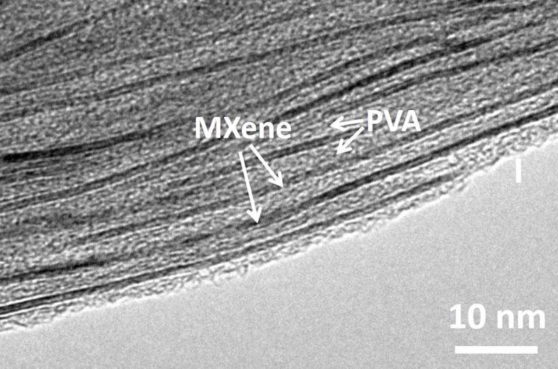
To produce the flexible conductive polymer nanocomposite, the researchers intercalated the titanium carbide MXene, with polyvinyl alcohol (PVA) –a polymer widely used as the paper adhesive known as school or Elmer’s glue, and often found in the recipes for colloids such as hair gel and silly putty. They also intercalated with a polymer called PDDA (polydiallyldimethylammonium chloride) commonly used as a coagulant in water purification systems.

“The uniqueness of MXenes comes from the fact that their surface is full of functional groups, such as hydroxyl, leading to a tight bonding between the MXene flakes and polymer molecules, while preserving the metallic conductivity of nanometer-thin carbide layers.  This leads to a nanocomposite with a unique combination of properties,” Gogotsi said.

The results of both sets of MXene testing were recently published in the Proceedings of the National Academy of Sciences. In the paper, the researchers report that the material exhibits increased ability to store charge over the original MXene; and 300-400 percent improvement in strength.

“We have shown that the volumetric capacitance of an MXene-polymer nanocomposite can be much higher compared to conventional carbon-based electrodes or even graphene,” said Chang Ren, Gogotsi’s doctoral student at Drexel. “When mixing MXene with PVA containing some electrolyte salt, the polymer plays the role of electrolyte, but it also improves the capacitance because it slightly enlarges the interlayer space between MXene flakes, allowing ions to penetrate deep into the electrode; ions also stay trapped near the MXene flakes by the polymer. With these conductive electrodes and no liquid electrolyte, we can eventually eliminate metal current collectors and make lighter and thinner supercapacitors.”

Though just a few atoms thick, the MXene-polymer nanocomposite material shows exceptional strength -especially when rolled into a tube.


The testing also revealed hydrophilic properties of the nanocomposite, which means that it could have uses in water treatment systems, such as membrane for water purification or desalinization, because it remains stable in water without breaking up or dissolving.

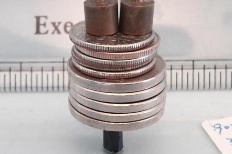
In addition, because the material is extremely flexible, it can be rolled into a tube, which early tests have indicated only serves to increase its mechanical strength. These characteristics mark the trail heads of a variety of paths for research on this nanocomposite material for applications from flexible armor to aerospace components. The next step for the group will be to examine how varying ratios of MXene and polymer will affect the properties of the resulting nanocomposite and also exploring other MXenes and stronger and tougher polymers for structural applications.

Freescale Semiconductor has been named a 2015 CES Innovation Awards Honoree for its Wearable Reference Platform (WaRP). WaRP is a community-based, Internet of Things platform offering designers unique product development flexibility in the quickly evolving consumer wearables market. It encourages design creativity by addressing key development challenges such as battery life, miniaturization, cost and usability.

Announced last night in New York City at the 2015 International CES Unveiled New York, the CES Innovation Awards is an annual competition honoring outstanding design and engineering in consumer technology products. Products entered in this prestigious program are judged by a preeminent panel of independent industrial designers, engineers and members of the trade media, to recognize cutting-edge consumer electronics products across 28 product categories.

An honoree in the Embedded Technologies category, WaRP is a flexible platform built on a hybrid architecture that enables systems designers to move from prototype to product quickly and easily for a broad range of fitness, healthcare and infotainment wearables. The system-level development kit supports embedded wireless charging, incorporates Freescale processors and sensors, and comes with open-source software, a battery and a touchscreen LCD module. WaRP is a result of collaboration among Freescale, CircuitCo, Kynetics and Revolution Robotics.

“We are proud to be among the chosen CES Innovation Honorees, and look forward to seeing many new, imaginative wearable products made possible by the WaRP platform,” said Sujata Neidig, consumer market business development manager for Freescale. “We also want to congratulate our customer and fellow awardee AMPL Labs for the creative use of Freescale technology they’ve packed into their SmartBackpack, which is a great example of adding intelligence to everyday items.”

Freescale customer AMPL Labs was named a 2015 CES Innovation Awards Honoree in the Portable Power and Computer Accessories categories. The company’s SmartBackpack provides connected, on-the-go consumers with a versatile portable charging system, advanced protection of electronics carried in the bag, and wireless connectivity with mobile devices.

Freescale’s Kinetis KL26 microcontroller enabled AMPL Labs to design the backpack’s intelligence, which monitors battery levels, controls power flow for charging devices and communicates with mobile devices using Bluetooth LE. The backpack also utilizes several Freescale sensors, including an accelerometer and pressure sensors. The Freescale Freedom Development Platform (FRDM-KL26Z) enabled AMPL Labs to prototype quickly and efficiently.

“We are honored to win this prestigious CES award and to highlight the innovative ways we are using Freescale chips, technology and tools to make common, everyday things smarter,” said Michael Patton, CEO of AMPL Labs.

Worldwide silicon wafer area shipments increased during the third quarter 2014 when compared to second quarter area shipments according to the SEMI Silicon Manufacturers Group (SMG) in its quarterly analysis of the silicon wafer industry.

Total silicon wafer area shipments were 2,597 million square inches during the most recent quarter, a 0.4 percent increase from the 2,587 million square inches shipped during the previous quarter. New quarterly total area shipments are 11.0 percent higher than third quarter 2013 shipments, according to SEMI.

“After reaching record levels in the second quarter, silicon wafer shipment volume growth plateaued during the most recent quarter,” said Hiroshi Sumiya, chairman of SEMI SMG and general manager of the Corporate Planning Department of Shin-Etsu Handotai Co., Ltd. “Year-to-date silicon volumes are 10 percent higher than the same period last year.”

Quarterly Silicon Area Shipment Trends


Million Square Inches


Q3 2013

Q2 2014

Q3 2014

Q1-Q3 2013

Q1-Q3 2014

Total

2,341

2,587

2,597

6,859

7,548

Semiconductor Silicon Shipments* – Millions of Square Inches

Silicon wafers are the fundamental building material for semiconductors, which in turn, are vital components of virtually all electronics goods, including computers, telecommunications products, and consumer electronics. The highly engineered thin round disks are produced in various diameters (from one inch to 12 inches) and serve as the substrate material on which most semiconductor devices or “chips” are fabricated.

All data cited in this release is inclusive of polished silicon wafers, including virgin test wafers, epitaxial silicon wafers, and non-polished silicon wafers shipped by the wafer manufacturers to the end-users.

The Silicon Manufacturers Group acts as an independent special interest group within the SEMI structure and is open to SEMI members involved in manufacturing polycrystalline silicon, monocrystalline silicon or silicon wafers (e.g., as cut, polished, epi, etc.). The purpose of the group is to facilitate collective efforts on issues related to the silicon industry including the development of market information and statistics about the silicon industry and the semiconductor market.

For more information on the SEMI Worldwide Silicon Wafer Shipment Statistics, visit www.semi.org/en/MarketInfo/SiliconShipmentStatistics.