By Debra Vogler, senior technical editor
February 23, 2011 — As gold becomes more expensive, copper wire bonding becomes more appealing for chip packaging. Reverse bonding, fine-pitch bonding, looping, second bonds, and other technologies are ramping on roadmaps, according to Kulicke & Soffa (K&S).
Bob Chylak, VP engineering, packaging & process integration at Kulicke & Soffa, was the featured speaker at a recent iMAPS NorCal chapter lunch meeting (Santa Clara, CA; 2/2/11). He covered the topic of converting from gold to copper for wire bonding — a move gaining ever greater interest by the surging price of gold. With heightened activities to close the knowledge gap with respect to using copper, many of the challenges have been addressed, observed Chylak.
Listen to Chylak’s interview: Download (iPhone/iPod users) or Play Now
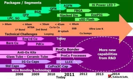
Laying out his company’s copper R&D roadmap (figure), Chylak noted that high-volume production of fine-pitch copper replacing gold already started in 2010. Advanced QFNs and stacked die still need to be developed, and LED packaging needs to be transitioned to copper, though Chylak noted that the challenge there will be with copper’s reflectivity not being as good as gold.
 |
|
Figure. Copper transition and roadmap planning. SOURCE: Kulicke & Soffa |
Chylak said that nearly the entire K&S process engineering staff is working on the copper transition. In particular, work is being done on reverse bonding and getting yields to 50ppm or less. "It’s mainly around the looping [for stacked dies] and second bonds [including for LEDs] we’re focusing on," said Chylak.
Subscribe to Solid State Technology/Advanced Packaging.
Follow Advanced Packaging on Twitter.com by clicking www.twitter.com/advpackaging. Or join our Facebook group


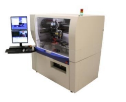
 Die Bonder, created for flexibility, high accuracy and precision.