Category Archives: Materials and Equipment

April 20, 2011 — SmartKem Limited, developer of novel, printable organic semiconductor materials and ink formulations for flexible electronics, received investment funding from the Porton Capital Group and Finance Wales Investments Limited. The investment allows SmartKem to further develop its flexible printed electronics solutions.

Based in Denbighshire, Wales, SmartKem develops a novel range of high mobility organic semiconductor molecules and ink formulations compatible with printed electronic processes. This is an inexpensive, low weight, low energy, alternative to silicon semiconductors and can be used to print organic circuits and devices onto thin flexible substrates such as plastics and paper.

SmartKem has just completed a key R&D phase and is focusing on the formulation of innovative organic semiconductor inks for improved performance and manufacturing of printed transistor arrays and logic circuits. The company targets electronic displays, thin-film RFID, smart sensors and printed logic circuit integration. The funding puts SmartKem at a definitive position in the microelectronics market.

Steve Kelly, CEO SmartKem, comments, “Our semiconductor materials are currently being sampled to a number of electronic device manufacturers and with this investment, SmartKem can scale up market testing and accelerate towards commercialization. This will allow us to further establish our position as a leading independent provider of organic semiconductor solutions for the printed electronics sector and to continue our breakthrough research and development projects.”

SmartKem is a high tech enterprise developing an new technology focusing on high performance/high value organic semiconductor materials that can be printed to form electronic circuits onto lightweight, rugged and low cost polymer films. For more information on SmartKem, visit www.smartkem.com.

Follow Small Times on Twitter.com by clicking www.twitter.com/smalltimes. Or join our Facebook group

April 20, 2011 — Boston Semi Equipment LLC (BSE Group) acquired the assets of Asia Tech Corporation, launching BSE Tech LLC. BSE Tech delivers a comprehensive portfolio of pre-owned front end semiconductor manufacturing equipment and spare parts, technical capabilities and financial solutions.

BSE Tech will facilitate the lease, sale, repositioning and servicing of all makes and models of new and pre-owned front end semiconductor equipment worldwide.

Combining these new assets with our OEM remarketing and partnership agreements is a competitive move, said Doug Elder, CEO and president of BSE Group. "BSE Group’s financial backing gives BSE Tech the ability to own its own equipment and the purchasing power to acquire new tools, which is a key differentiator in this market."

BSE Tech has signed a long-term lease for a 75,000 square foot facility in Tempe, AZ, doubling the former footprint of Asia Tech. The new location will also house a new 15,000 square foot cleanroom, currently under construction. Asia Tech’s president, Francis Colligan, will join BSE Tech in the role of vice president. All employees of Asia Tech are now part of BSE Tech.

BSE Tech LLC (BSE Tech) is a global supplier of pre-owned front end semiconductor manufacturing equipment. BSE Tech buys, reconfigures, finances and sells a broad range of front end wafer fabrication equipment including all makes, models and vendors. It also offers spare parts and pumps from all of the major OEMs as well as third party manufactured goods. Boston Semi Equipment LLC (BSE Group) provides affordable solutions to semiconductor front end manufacturing and back end assembly and test through leasing, rental, and resale of equipment. For more information visit http://www.bsegroup.com.

Also read: Secondary semiconductor equipment market is complex, and growing

Subscribe to Solid State Technology/Advanced Packaging.

Follow Solid State Technology on Twitter.com via editors Pete Singer, twitter.com/PetesTweetsPW and Debra Vogler, twitter.com/dvogler_PV_semi.

Or join our Facebook group

April 19, 2011 — Plasmonics, a phenomenon in which the confinement of light in dimensions smaller than the wavelength of photons in free space make it possible to match the different length-scales associated with photonics and electronics in a single nanoscale device, has become one of the hottest fields in high-technology. However, to date plasmonic properties have been limited to nanostructures that feature interfaces between noble metals and dielectrics. Now, researchers with the U.S. Department of Energy (DOE)’s Lawrence Berkeley National Laboratory (Berkeley Lab) have shown that plasmonic properties can also be achieved in the semiconductor nanocrystals known as quantum dots.

"We have demonstrated well-defined localized surface plasmon resonances arising from p-type carriers in vacancy-doped semiconductor quantum dots that should allow for plasmonic sensing and manipulation of solid-state processes in single nanocrystals," says Berkeley Lab director Paul Alivisatos, a nanochemistry authority who led this research. "Our doped semiconductor quantum dots also open up the possibility of strongly coupling photonic and electronic properties, with implications for light harvesting, nonlinear optics, and quantum information processing."

Alivisatos is the corresponding author of a paper in the journal Nature Materials titled "Localized surface plasmon resonances arising from free carriers in doped quantum dots." Co-authoring the paper were Joseph Luther and Prashant Jain, along with Trevor Ewers.

Plasmonics could enable faster, higher-volume chip interconnects, microscope lenses that resolve nanoscale objects with visible light, highly efficient light-emitting diodes (LEDs), and supersensitive chemical and biological detectors. There is evidence that plasmonic materials can be used to bend light around an object, rendering that object invisible.

The plasmonic phenomenon was discovered in nanostructures at the interfaces between a noble metal, such as gold or silver, and a dielectric, such as air or glass. Directing an electromagnetic field at such an interface generates electronic surface waves that roll through the conduction electrons on a metal, like ripples spreading across the surface of a pond that has been plunked with a stone. Just as the energy in an electromagnetic field is carried in a quantized particle-like unit called a photon, the energy in such an electronic surface wave is carried in a quantized particle-like unit called a plasmon. The key to plasmonic properties is when the oscillation frequency between the plasmons and the incident photons matches, a phenomenon known as localized surface plasmon resonance (LSPR). Conventional scientific wisdom has held that LSPRs require a metal nanostructure, where the conduction electrons are not strongly attached to individual atoms or molecules. This has proved not to be the case.

Prashant Jain, a member of the Alivisatos research group and one of the lead authors of the Nature Materials paper, explains, "Our study represents a paradigm shift from metal nanoplasmonics as we’ve shown that, in principle, any nanostructure can exhibit LSPRs so long as the interface has an appreciable number of free charge carriers, either electrons or holes. By demonstrating LSPRs in doped quantum dots, we’ve extended the range of candidate materials for plasmonics to include semiconductors, and we’ve also merged the field of plasmonic nanostructures, which exhibit tunable photonic properties, with the field of quantum dots, which exhibit tunable electronic properties. Unlike a metal, the concentration of free charge carriers in a semiconductor can be actively controlled by doping, temperature, and/or phase transitions. Therefore, the frequency and intensity of LSPRs in dopable quantum dots can be dynamically tuned. The LSPRs of a metal, on the other hand, once engineered through a choice of nanostructure parameters, such as shape and size, is permanently locked-in."

Jain and his co-authors made their quantum dots from the semiconductor copper sulfide, a material that is known to support numerous copper-deficient stoichiometries. Initially, the copper sulfide nanocrystals were synthesized using a common hot injection method. While this yielded nanocrystals that were intrinsically self-doped with p-type charge carriers, there was no control over the amount of charge vacancies or carriers.

"We were able to overcome this limitation by using a room-temperature ion exchange method to synthesize the copper sulfide nanocrystals," Jain says. "This freezes the nanocrystals into a relatively vacancy-free state, which we can then dope in a controlled manner using common chemical oxidants."

By introducing enough free electrical charge carriers via dopants and vacancies, Jain and his colleagues were able to achieve LSPRs in the near-infrared range of the electromagnetic spectrum.

Jain envisions quantum dots as being integrated into a variety of future film- and chip-based photonic devices that can be actively switched or controlled, and also being applied to such optical applications as in vivo imaging.

In addition, the strong coupling that is possible between photonic and electronic modes in such doped quantum dots holds exciting potential for applications in solar photovoltaics and artificial photosynthesis. "In photovoltaic and artificial photosynthetic systems, light needs to be absorbed and channeled to generate energetic electrons and holes, which can then be used to make electricity or fuel," Jain says. "To be efficient, it is highly desirable that such systems exhibit an enhanced interaction of light with excitons. This is what a doped quantum dot with an LSPR mode could achieve."

The potential for strongly coupled electronic and photonic modes in doped quantum dots arises from the fact that semiconductor quantum dots allow for quantized electronic excitations (excitons), while LSPRs serve to strongly localize or confine light of specific frequencies within the quantum dot. The result is an enhanced exciton-light interaction. Since the LSPR frequency can be controlled by changing the doping level, and excitons can be tuned by quantum confinement, it should be possible to engineer doped quantum dots for harvesting the richest frequencies of light in the solar spectrum.

Quantum dot plasmonics also hold intriguing possibilities for future quantum communication and computation devices. "The use of single photons, in the form of quantized plasmons, would allow quantum systems to send information at nearly the speed of light, compared with the electron speed and resistance in classical systems," Jain says. "Doped quantum dots by providing strongly coupled quantized excitons and LSPRs and within the same nanostructure could serve as a source of single plasmons."

Jain and others in Alivsatos’ research group are now investigating the potential of doped quantum dots made from other semiconductors, such as copper selenide and germanium telluride, which also display tunable plasmonic or photonic resonances. Germanium telluride is of particular interest because it has phase change properties that are useful for memory storage devices.

"A long term goal is to generalize plasmonic phenomena to all doped quantum dots, whether heavily self-doped or extrinsically doped with relatively few impurities or vacancies," Jain says.

This research was supported by the DOE Office of Science.

Lawrence Berkeley National Laboratory addresses the world’s most urgent scientific challenges by advancing sustainable energy, protecting human health, creating new materials, and revealing the origin and fate of the universe. Founded in 1931, Berkeley Lab’s scientific expertise has been recognized with 12 Nobel prizes. The University of California manages Berkeley Lab for the U.S. Department of Energy’s Office of Science. For more, visit www.lbl.gov.

For more information about the research of Paul Alivisatos, visit the Website at http://www.cchem.berkeley.edu/pagrp/

For more information about the research of Prashant Jain, visit the Website at http://www.nanogold.org/

Follow Small Times on Twitter.com by clicking www.twitter.com/smalltimes. Or join our Facebook group

April 18, 2011 – BUSINESS WIRE — Agilent Technologies Inc. (NYSE:A) delivered a fully integrated 1.1-THz network analysis measurement solution to Japan’s Yamaguchi University. The solution will play a critical role in enabling the university to study metamaterials at THz frequencies.

Click to Enlarge

The THz region of the electromagnetic spectrum has enormous potential for high-data-rate communications, advanced electronic materials spectroscopy, space research, medicine, biology, surveillance and remote sensing. Despite its potential, the THz region remains one of the most unexplored areas of the spectrum. And, since high-power THz sources rely heavily on materials with advantageous properties in the THz frequency range, materials research is a critical component of modern THz systems.

Agilent’s integrated measurement solution addresses this challenge by enabling accurate measurement of THz signals in new materials. Such information is critical to the successful resolution of Yamaguchi University’s materials research.

Agilent’s solution features a fully calibrated, 750-GHz to 1.1-THz frequency extension module, the WR-01, from Virginia Diodes Inc., coupled with Agilent’s high-performance 50-GHz PNA-X vector network analyzer. Together, these tools allow for a fully calibrated, vector network analysis measurement with greater than 50dB of dynamic range.

Users can take advantage of the PNA-X’s calibration technology to make stable and repeatable THz measurements. The instrument’s dynamic range also ensures that users can easily achieve highly sensitive measurements. And, with the frequency extension module’s ability to operate across the 750-GHz to 1.-THz frequency range, users can now easily capture higher resolution images as well.

"At Virginia Diodes, our mission is to make the THz region of the electromagnetic spectrum as useful for scientific, military and commercial applications as the microwave and infrared bands are today," said Thomas Crowe, chief executive officer of Virginia Diodes. The WR-01 extender offers the dynamic range and bandwidth required for THz-calibrated vector network analyzer measurements, Crowe added.

"Working closely with Virginia Diodes, we were able to integrate the WR-01 extender into our PNA-X vector network analyzer, further extending its capabilities and enabling fast and accurate measurements at THz," said Gregg Peters, vice president and general manager of Agilent’s Component Test Division.

Agilent Technologies Inc. (NYSE: A) provides tools for chemical analysis, life sciences, electronics and communications. Information about Agilent is available at www.agilent.com. Agilent’s PNA-X vector network analyzer provides the industry’s widest range of measurement applications, from RF to millimeter wave. More information about the PNA-X is available at www.agilent.com/find/pna-x

Yamaguchi University is located in Ube-city, Japan. Its characterization of materials at THz frequencies is part of an ongoing effort within the school of science and engineering. For more information, go to http://www-ap.apsci.yamaguchi-u.ac.jp/groups/appliedphysicslaboratory/

Follow Small Times on Twitter.com by clicking www.twitter.com/smalltimes. Or join our Facebook group

Longtime semiconductor exec Takeshi Hattori continues his reporting on the aftermath of the massive Japanese earthquake and tsunami, with updates on the nuclear crisis, status of facilities and production struggles. See previous updates from Japan here, here, here, and here.

April 18, 2011 – The nuclear crisis is ongoing, ranked up to Level 7 last week, on the International Nuclear Event Scale (INES), the scale’s highest level, and equal to the 1986 Chernobyl nuclear disaster.

Click to EnlargeUpon a strong request by the Japanese Government, Tokyo Electric Power Company (TEPCO), owner/operator of Fukushima Daiichi nuclear plant, released yesterday (Sunday, April 17) a roadmap or timetable to have the nuclear crisis under control, which will take six to nine months. On the same day, US Secretary of State Hillary Clinton made a short (five hour) visit to Tokyo to pledge full American support to help Japan recover from the March 11 earthquake and tsunami. The rolling blackouts are over, but shortage of ultrapure hydrogen peroxide as well as silicon wafers may slow semiconductor manufacturing in Japan (see below).

TEPCO outlined a two-step scenario to bring the nuclear reactors under control. The first action would be to cool the reactors in a stable manner and prevent water with high levels of radioactivity from flowing out of the plant over the next three months. The second step is to reduce the amount of radiation being created by restoring the plant’s cooling system so that cooling water can be recirculated. Following these two steps within six to nine months, the company hopes to be able to bring the four reactors (made by GE/Toshiba/Hitachi) to a "cold shutdown" in which the temperatures at reactor cores are kept under 100°C.

After TEPCO’s announcement, MITI minister Kaieda said Sunday the government hopes to inform evacuees near the nuclear plant in Fukushima prefecture in six to nine months whether they can return home — but many evacuees claimed that the TEPCO roadmap is just a challengeable target, or "pie in the sky." Foreign Affairs minister Matsumoto asked Hillary Clinton, in Tokyo, to bring back the TEPCO roadmap to the US to critically evaluate by nuclear experts there.

Prime minister Kanno said today, through debate in the Diet [Japan’s legislative body], that future nuclear plant expansion program in Japan will be freezed. He also pointed out that it should be abolished that high-ranking MITI officials get executive positions at TEPCO and other electric power companies after their retirements.

A global team led by Hitachi and GE said last week that it would take at least three decades to make the nuclear reactors to be decommissioned and then to return the site to what the firms refer to as a "green field" state within legal limits of radiation for any residents. Toshiba said it could take at least 10 years.

Scheduled rolling blackouts in East Japan is virtually over, because spring has come with cherry blossoms and become warmer; also, everybody is making every effort to save electricity consumption everywhere (at home, offices, fabs, stores, and even at airports and train stations.) Some companies employ their own "summer time" (one-hour shift of their office hours) schedules: fab operations at night, national holidays and/or weekends, and one or two week fab shutdown in the peak summer with employees’ longer summer vacations all at once.

Shortages in key semiconductor materials

Semiconductor manufacturing in Japan is starting to expose a shortage of hydrogen peroxide (liquid) for standard silicon wafer cleaning and photoresist removal, as well as anticipated bulk-silicon wafer shortage in the very near future. According to Japanese industry sources, epitaxial silicon wafers has already been in shortage.

Hydrogen peroxide

The hydrogen peroxide (H2O2) plant of Tokyo-based Mitsubishi Gas Chemical Company (MGC) in Kashima, Ibaraki Prefecture, has stopped production due to infrastructural damage of the Kashima water-front industrial complex since March 11. This plant produces 104,000 tons of hydrogen peroxide annually, almost half of the domestic demand in Japan. The plant’s share of ultrapure hydrogen peroxide for silicon wafer cleaning and photoresist removal is some 60% in the Japanese semiconductor industry.

As of March 11, MGC had been accumulating its stockpiles to exceed one-month levels to prepare the scheduled maintenance/repair of the whole plant in this May-June timeframe. The plant will become partial operational within this month, but a plant shutdown for scheduled repair will be unavoidable, so the shortage is anticipated next month. In the end market the shortage is already a reality, and this is presently the major concern for semiconductor fab managers.

MGC is preparing to urgently import ultrapure (semiconductor-grade) hydrogen peroxide from some or all of their group manufacturing companies to produce it in Korea, Taiwan, Singapore, and the US, as well as general-purpose H2O2 from their group firms in China and Indonesia. MGC may even purchase H2O2 from companies outside the group worldwide, depending the shortage situation.

MGC had announced a severe control of shipments (probably shipping only 30% of the total orders) starting from the middle of April, but it was postponed to early May, with possible 70%-80% shipment of the total orders if the H2O2 imports will be timely done.

Silicon wafers

Shin-Etsu Hantodai’s Shirakawa plant in Fukushima Prefecture, the world largest 300mm wafer manufacturing base, expects to resume partial operation by the end of this month, but it is not clear when the facility will restart production as of today. If they cannot resume operation for several more weeks, the wafer shortage issue will become clear.

MEMC Electronic Materials has resumed production of 300mm wafers at its facility in Utsunomiya, Tochigi Prefecture. The facility has been shipping unaffected product and has resumed production on qualified process tools, while continuing to inspect, qualify, and ramp additional equipment. Full 300mm production is targeted for the middle of May. The facility’s small volume of 200mm wafer capacity, previously scheduled to be moved to the company’s Ipoh, Malaysia site during the third quarter of 2011, is being moved ahead of the original schedule.

SUMCO’s Yonezawa plant in Yamagata prefecture has resumed operation but very partially.

Toshiba

Iwate Toshiba Electronics, in Kitakami, Iwate Prefecture, resumed partial operation today (April 18) instead of formerly announced April 11. The one-week delay was due to continuous aftershocks and subsequent blackouts reported previously. Toshiba Mobile Display’s Fukaya plant in Saitama Prefecture, which restarted partial operation on March 28, will become fully operational at the end of this month.


Takeshi Hattori is president of Hattori Consulting International and editorial columnist of Electronic Journal in Japan, with more than 36 years experience in the semiconductor field. He is a Fellow of the Electrochemical Society, founding member of the International Symposium on Semiconductor Manufacturing, member of SEMI’s Japan regional standards committee and SEMI/SEAJ Forum, and The Confab advisory board, among many others.

April 15, 2011 — Researchers at Eindhoven University of Technology have developed a replacement for indium tin oxide (ITO), which is used in displays, solar cells, and other technologies. This transparent, conducting film is produced in water, and based on electrically conducting carbon nanotubes (CNT) and plastic nanoparticles. The component materials are commonly available and the process is deemed environmentally friendly.
 

Click to Enlarge
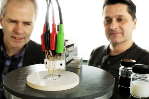
Image. 4-point conductivity measurement of the new transparent conducting film developed by Prof. Cor Koning (left) and prof. Paul van der Schoot (right). The black pot contains a dispersion of carbon nanotubes in water, and the white pot contains the conducting latex. Photo: Bart van Overbeeke.

The research team has been able to achieve higher conductivity by combining low concentrations of carbon nanotubes and conducting latex in a low-cost polystyrene film. The nanotubes and the latex together account for less than 1% of the weight of the conducting film (a high concentration of CNTs makes the film black and opaque). The research team was led by theoretical physicist Paul van der Schoot and polymer chemist Cor Koning. Post-doc Andriy Kyrylyuk is the first author of the paper in Nature Nanotechnology (see below).

The researchers use standard, widely available CNTs, which they dissolve in water. Then they add conducting latex (a solution of polymer beads in water), together with a binder in the form of polystyrene beads. When the mixture is heated, the polystyrene beads fuse together to form the film, which contains a conducting network of nanotubes and beads from the conducting latex. The water, which only serves as a dispersing agent in production, is removed by freeze-drying. The researchers calculated the expected effects and also understood how the increased conductivity worked before trying the formula.

The conductivity of the transparent film is still a factor 100 lower than that of indium tin oxide. But Van der Schoot and Koning expect that the gap can quickly be closed. Standard CNTs are a mixture of metallic conducting and semiconducting tubes, notes Cor Koning. "As soon as you start to use 100% metallic tubes, the conductivity increases greatly. The production technology for 100% metallic tubes has just been developed, and we expect the price to fall rapidly."

The film’s conductivity is already good enough to be used immediately as an antistatic layer for displays, or for EMI shielding to protect devices and their surroundings against electromagnetic radiation.

The film has an important advantage over ITO: it is environment-friendly. All the materials are water-based, and no heavy metals such as tin are used. The new film is also a good material for flexible displays.

The research team was a combination of theoreticians, modeling specialists and staff to do practical experiments.

The results, which also provide new insights into conduction in complex composite materials, were published online April 10 by the scientific journal Nature Nanotechnology, "Controlling Electrical Percolation in Multi-Component Carbon Nanotube Dispersions" (DOI: 10.1038/NNANO.2011.40). Access it here: http://www.nature.com/nnano/journal/vaop/ncurrent/full/nnano.2011.40.html

The research forms part of the Functional Polymer Systems research program at the Dutch Polymer Institute (DPI), which provided financial support for this project. Prof. Cor Koning is with the Polymer Chemistry group (Department of Chemical Engineering and Chemistry) and prof. Paul van der Schoot is with the Theory of Polymers and Soft Matter group (Department of Applied Physics) of Eindhoven University of Technology. The other authors of the article are Andriy Kyrylyuk (first author), Marie Claire Hermant, Tanja Schilling and Bert Klumperman.

Subscribe to Solid State Technology/Advanced Packaging.

Follow Solid State Technology on Twitter.com via editors Pete Singer, twitter.com/PetesTweetsPW and Debra Vogler, twitter.com/dvogler_PV_semi.

Or join our Facebook group

April 15, 2011 — Electron microscopes use focused electron beams to make extremely small objects visible. By combining the microscope with a gas-injection system, material samples can be manipulated and nanometer-wide surface structures can be written. Empa researchers, together with scientists from EPFL, used this method to improve lasers.

The vertical cavity surface emitting laser (VCSEL), a semiconductor laser often used in data transmission for short-distance links like Gigabit Ethernet, exhibits one weakness: Because of the cylindrical structure in which the lasers are built up on the wafer, the polarization of the emitted light can sometimes change during operation. Stable polarization is necessary to reduce transmission errors and to use VCSELs in future silicon photonics.

Click to Enlarge

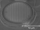
Image: The result is a nanostructure — for example, a polarization grating on a VCSEL (vertical cavity surface emitting laser). These are semiconductor lasers frequently used in optical data transmission.

"We’ve written flat grating structures on the VCSELs with an electron beam," says Ivo Utke, Empa researcher, in describing their solution, "and the gratings were effective in stabilizing the polarization."

Click to Enlarge

Image. The principle of the local deposition process, which is induced with a focused electron beam (FEBIP), is that molecules from a gas-injection system are deposited on the sample surface in a reversible manner. The focused electron beam dissociates adsorbed gas molecules. The resulting non-volatile compounds remain permanently on the sample.

Minimally invasive, direct FEBIP is suitable for prototyping nanocomponents to solve specific questions and problems in applied nanoelectronics, nanophotonics, and nanobiology. Suitable gas molecules are injected close to a sample which is already in the microscope’s vacuum chamber. These adsorb on the sample in a reversible manner.

The focused electron beam induces chemical reactions of the adsorbed gas molecules, but only at the spot where the beam strikes the surface. The resulting non-volatile molecular fragments then remain permanently on the sample while the volatile fragments are removed by the vacuum system. "With the help of a precisely positioned electron beam, it’s possible to remove or apply surface structures with nanometer precision and in virtually any desired three-dimensional shapes, explains Utke. "FEBIP could soon become a true nanofabrication platform for rapid prototyping of nanostructures in a minimally invasive way, without necessitating the large investment of a clean room."

The team was led by Utke, together with scientists from the Laboratory of Physics of Nanostructures at EPFL. The study has recently been published in the scientific journal Nanoscale as an advanced online publication. Access the article here.

Learn more at www.empa.ch

Follow Small Times on Twitter.com by clicking www.twitter.com/smalltimes. Or join our Facebook group

April 15, 2011 – PR Newswire — EoPlex Technologies Inc. is promoting the xLC substrate for quad flat pack no lead (QFN) semiconductor packages. The substrate enables QFNs with hundreds of leads and multiple rows at a lower cost than conventional packages.

The EoPlex xLC substrate is a sintered metal array of wire bond and die attach pads delivered on a temporary thin metal strip (the lead carrier). The product is designed to be a direct replacement for the leadframe and is completely compatible with all QFN processing. With EoPlex xLC, packages can be made with as many rows as needed with hundreds of leads. xLC production is based on sintering for better environmental friendliness.

QFNs are the fastest growing packaging segment; however, they cannot be used in many applications due to the limitations imposed by the metal leadframe that is used to build them. The most critical limitation is that the leadframe prevents multi-row and high-lead-count designs, which are currently served by BGAs, says EoPlex. The leadframe also makes QFNs bigger than necessary, adds extra metal that reduces electrical performance, requires expensive polyimide tape and can slow down process steps like dicing and testing.

By using space efficiently and adding no waste metal, the substrate allows up to 50% more package-sites on each strip, resulting in a price per package-site that is 20-30% less than leadframes, said Arthur L. Chait, CEO of EoPlex.

EoPlex is a private company backed by Draper Fisher Jurvetson, ATA Ventures, Labrador Ventures and Draper-Richards. More information is at www.eoplex.com.

Subscribe to Solid State Technology/Advanced Packaging.

Follow Advanced Packaging on Twitter.com by clicking www.twitter.com/advpackaging. Or join our Facebook group

April 13, 2011 — SEMI and Semico announced the Secondary Semiconductor Equipment Market Study, which estimates that secondary market equipment sales reached $6.0 billion in 2010, a 77% increase over 2009. At 13% of the total equipment spending for semiconductor manufacturing, secondary equipment and services are gaining importance at both 300 and 200mm fabs.

The study was initiated by the Secondary Equipment, Services & Technology Group (SESTG), a special interest group of SEMI, with participation from the full spectrum of the secondary equipment market: IDMs, foundries, equipment OEMs, finance and lease companies, refurbishers and brokers.

The current market is complex, which makes the secondary semicondustor equipment sector difficutt to measure, noted Dan Tracy, senior director, Industry Research & Statistics at SEMI, "Secondary semiconductor equipment is refurbished and sold through a variety of different players; it is a highly fragmented supply chain.  In addition to the original equipment manufacturers, semiconductor manufacturers, refurbishers, dealers and brokers also buy and sell equipment.  One piece of equipment can change hands several times before it is put back into a production or research facility."

The Secondary Semiconductor Equipment Market Study is based on a combination of primary research and secondary data analysis. SEMI/SESTG, in collaboration with Semico Research Corp., conducted surveys of the secondary equipment community.  Participants included IDMs, foundries, OEMs (equipment suppliers), equipment brokers, dealers and refurbishers. Primary data was supplemented with information from company financial reports, company analyst presentations as well as Semico Research Corp.’s databases including capital expenditures, semiconductor fabs, and wafer demand. SEMI and Semico have an extensive network of contacts ranging from executives to engineers at semiconductor manufacturers and semiconductor equipment vendors.  The information in this study was developed from surveys, interviews and briefings by these contacts and from ongoing conversations with the contacts.

The study estimates the secondary equipment market by region, by wafer size, by equipment type, and by vendor type. The study can be used to help companies improve business planning, market share and sales analysis, investment sourcing, resource allocation, and new product development. It can be purchased in SEMI’s store.

SEMI is the global industry association serving the manufacturing supply chains for the microelectronic, display and photovoltaic industries. For more information, visit www.semi.org. Read SEMI’s blog, SEMI News and Views

Semico Research Corp is a semiconductor marketing and consulting research company. For more information, visit www.semico.com.

Subscribe to Solid State Technology/Advanced Packaging.

Follow Solid State Technology on Twitter.com via editors Pete Singer, twitter.com/PetesTweetsPW and Debra Vogler, twitter.com/dvogler_PV_semi.

Or join our Facebook group

April 13, 2011 — Questar Products International, a manufacturer of automatic wire bonders for the global assembly market, released the Q7000 series of fine-pitch, fine-wire (17-75μm), aluminum/gold (Al/Au) automatic wedge and ball bonders to better meet smaller lot size, multiple product variation, frequent set-up change styles of package production.

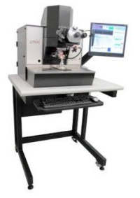
Click to EnlargeThe Q7000 Series has updated hardware and software, delivering a more tightly integrated assembly package, with approximately 30% fewer components and 50% less wiring than the Q2100 Series, which it replaces. These systems also cost less than the Q2100 models. The machines are designed with off-the-shelf components available directly from suppliers worldwide.

In addition, Questar has simplified the configuration selection process by including previously optional items, such as a programmable ultrasonic generator, as standard features.

Also standard is ball/stud bumping, stitch bonding, and table tear for wedge bonding. The customer chooses the appropriate heated or ambient workholder (and a programmable temperature controller if gold wire is to be used with the Q7800 wedge bonder) when ordering a Q7000 or Q7800 wire bonding system.

These automatic wire bonders support prototyping to medium-volume production. Designed for packaging applications from basic monolithic to complex hybrid devices and custom, specialty systems, the Q7000 series accommodates a multitude of device configurations. Package conversions are reportedly simple and can be completed in minutes.

The new design has also placed all control electronics on the top of the bonders for easier, no-tools-required access.

Questar Products offers hardware and software customization for specialty device applications such as unique wire-shaping and larger bondable area requirements.

Running on the Windows XP Pro operating system, the Q7000 Series offers intuitive, menu-driven software that is easy to program, with convenient access to all machine functions. The user-friendly operator interface provides point-and-click bonding; unlimited wires; easy bond process editing; extensive program storage; and a bond parameter library.

Questar provides wire-bonding machines to the global solid-state component assembly market. For more information on the Q7000 Series, visit www.questarproducts.com.

Subscribe to Solid State Technology/Advanced Packaging.

Follow Advanced Packaging on Twitter.com by clicking www.twitter.com/advpackaging. Or join our Facebook group