Category Archives: Materials and Equipment

by Dr. Phil Garrou, contributing editor

March 22, 2011 – The recent IMAPS Global Business Council (GBC) Meeting and Device Packaging Conference (DPC) was the source of some significant new developments in the areas of 3D IC and fan-out wafer-level packaging.

Matt Nowak, senior director at Qualcomm, reviewed the key attributes of 3D ICs, including performance enhancement, improved power efficiency, form factor miniaturization, and cost reduction. From there, a question arises — can 3D ICs can take the place of scaling as CMOS technology appears to be slowing (or stalling)? He concludes:

  • Yes — if performance enhancement and power reduction are the primary motivation.
  • Yes — if form factor miniaturization is the only motivation.
  • No — if cost reduction is the primary motivation. (However, 3D with TSVs can provide cost reduction benefits, if cost improvements derived from CMOS scaling diminish in future nodes, e.g. due to advanced lithography and FEOL costs.)

Sitaram Arkalgud, director of SEMATECH’s 3D IC program, shared the organization’s perspective on the readiness of 3D IC toolsets:

Click to Enlarge

Taiji Sakai of Fujitsu indicated that the demand for tighter-pitch bonding has moved the industry to copper pillar bumping but that the time/temp bonding requirements of direct Cu-Cu bonding is keeping companies from moving to that technology despite its electrical performance advantages.

Click to Enlarge

He revealed that if the Cu bumps are planarized by cutting with a diamond bit vs. the normal CMP process, a "amorphous-like layer" is produced at the surface which allows Cu-Cu direct bonding at 200-250°C (30min) vs. the >350°C (30min) required for a CMP’ed surface.

Paul Siblerud of Applied Materials announced that EMCD 3D consortium members, having met their goal of $150/wafer, will be ending the consortium this coming summer.

Rumors going around at this years IMAPS-DPC were concerned with interposers reportedly failing in thermal cycling (TC) reliability tests. Reports are that when the interposers are populated with unequal size or thickness silicon chips or chip stacks, the stresses generated on the interposers during TC causes the interposers to break. Ron Huemoeller, VP of 3D packaging for Amkor, confirmed that this indeed was an issue, but that Amkor had been able to engineer around it. He also revealed that the underfill process for the Xilinx program took more than a year get to a reliable, manufacturable state.

At the GBC, Suresh Ramalingam of Xilinx discussed their stacked silicon interconnect technology (SSIT). The 28nm Virtex-7 SSIT will reportedly use TSMC fabricated 100μm thick silicon interposers with 10-12μm Cu TSV and 65nm interconnect. The micro-bumps are Cu-SnAg alloys at 45μm pitch.

Click to Enlarge

Amkor’s Huemoeller also offered the following roadmap for memory stack usage:

Click to Enlarge

During an excellent panel session on fan-out packaging, Thorsten Meyer, one of the developers of the Infineon eWLB fan-out technology, informed the audience that his group was now part of the "Intel Mobile Communications" division, but that Infineon retains rights to non-wireless applications.

Navjot Chhabra, director of advanced packaging for the Freescale RCP fan-out program, indicated that they are in qualifications with "industrial and automotive products."

Tom Strothman, director of business development for STATS ChipPAC, indicated that eWLB is today less costly than FcBGA.

While STATS is currently running a 300mm line for production of eWLB, John Hunt, director of engineering for ASE, commented that "demand just does not warrant putting 300mm capacity in place." It was revealed that Infineon is the only commercial customer for eWLB today, with ST Micro being very close.

While all of the eWLB licensees are proposing fan-out packaging on panels, Hunt commented that ASE was "the only company who has tried to do this […] I can tell you that if we move forward with this approach it will require a totally new materials set." He indicated that they are attempting this work on 1/4 panels, not full PWB panels, and that obviously they cannot use molded underfill (MUF) to encapsulate the large substrates.


Dr. Phil Garrou is an IEEE Fellow and consultant with Microelectronic Consultants of NC.

March 21, 2011 – Semiconductor equipment demand inched back up in February, though part of that recovery was because January final numbers were a little softer than originally tallied, according to the latest monthly update from SEMI.

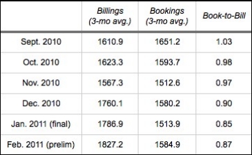
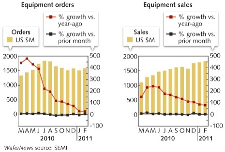
For February, North America-based manufacturers of semiconductor equipment reported $1.58B in bookings, up nearly 5% from January and 27% from a year ago. Billings were ~$1.83B, up around 2% month/month and nearly 80% from a year ago.

Click to Enlarge

A look inside the February 2011 numbers:

  • It’s been an up-and-down few months for chip tool demand: a 4% orders increase in December, then a -3% decline in January, and now a nearly 5% bounceback in February. Bookings have been in the $1.5B-$1.6B range for six months now… is this the new normal?
  • Billings have increased for three straight months now, adding about $260M in sales (nearly 17% growth). back off a December surge to a small 2.5% increase to $1.80B. They’re closing in on levels not seen since the spring of 2001 (only about 10% away, or $190M).
  • In revising its January figures, SEMI actually added subtracted about $22M in bookings and $17.5M in sales.
  • The book-to-bill ratio climbed slightly to 0.87, meaning $87 worth of orders received for every $100 billed. That’s a trend of less business coming in than going out, though at a slightly better rate than it was. We’re now five months below the 1.0 parity mark.
Click to Enlarge
Click to Enlarge

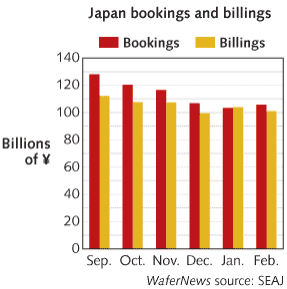
Normally we report Japanese semiconductor equipment data along with the SEMI North American data, since they are released at about the same time — but with the Japanese earthquake tragedy, the SEAJ has postponed its data reporting by a week until 3/25. We’ll update this story when the new data arrives.


Update:  The SEAJ’s delayed February numbers showed possible signs of life in semiconductor equipment demand. Orders rose about 2% from January (about 23% Y/Y) to ¥105.79B (US $1.305B), the first increase in five months. Sales slipped about -3% (+56% Y/Y) to ¥100.92B ($1.245B). That pushed the B:B back above parity to 1.05.

Click to Enlarge

March 17, 2011 – BUSINESS WIRE — The System LSI Division of Samsung Electronics Co. Ltd. has licensed the OptiML Zoom image enhancement solution from Tessera Technologies Inc. (NASDAQ:TSRA). Camera modules incorporating this technology enable high-quality zoom functionality in cell phones, portable video recorders and other camera-equipped mobile devices.

OptiML Zoom technology combines a non-mechanical lens designs with specialized algorithms to provide high-performance zoom with better reliability and manufacturability, says Tessera.

"Samsung has been offering high-quality CMOS imagers to the market place, and the cell phone market demands not only crisp, clear images, but also more advanced imaging technologies like 3X zoom," said Dojun Rhee, vice president, marketing team, System LSI Division, Samsung Electronics.

"Industry partners like Samsung LSI are crucial for executing our vision for implementing advanced imaging technologies in mobile devices," said John Keating, senior vice president, Tessera.

The OptiML family of image enhancement products from Tessera enables significantly higher quality images in a cell phone camera form factor without the need for mechanical parts, resulting in a more reliable, miniaturized, cost-effective solution. The OptiML Zoom solution offers 3X zoom capabilities, and the OptiML Focus solution enables all objects from 20cm to infinity to be in focus at once. The OptiML Low Light solution improves performance in low light, one of the key challenges in cell phone cameras, by increasing the amount of available light by as much as 250%, without degrading the field depth or other performance factors.

Tessera Technologies Inc. develops, invests in, licenses and delivers innovative miniaturization technologies and products for next-generation electronic devices. For information, go to www.tessera.com.

Subscribe to Solid State Technology/Advanced Packaging.

Follow Advanced Packaging on Twitter.com by clicking www.twitter.com/advpackaging. Or join our Facebook group

March 16, 2011 – BUSINESS WIRE — Scientists in GE’s Global Research Center have demonstrated an advanced thermal material system that could pave the way to faster computing and higher performing electronic systems. Leveraging technologies developed under GE’s Nanotechnology Advanced Technology Program, they have fabricated a prototype substrate that can cool electronic devices better than copper.

 Click to Enlarge
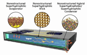
Figure. A diagram of GE’s advanced thermal material system. Leveraging unique surface engineered coatings that both repel and attract water, GE’s system achieves twice the heat conducting properties of copper and can function under extreme forces of gravity.

The development of GE’s prototype substrate, which utilizes phase-change-based heat transfer, is part of a 4-year, $6 million program funded by the Defense Advanced Research Program Agency (DARPA, Contract # No. N66001-08-C-2008). GE Global Research has been collaborating with GE Intelligent Platforms, the Air Force Research Laboratory, and University of Cincinnati on the project.

GE’s phase-change based prototype substrate can be applied to computer chips and different electronic components. It acts as a cooling mechanism that spreads or dissipates the heat generated in electronic systems to keep components cool.

"In demonstrations, GE’s prototype substrate has functioned effectively in a variety of electronics application environments. We also subjected it to harsh conditions during testing and found it could successfully operate in extremely high gravity applications," said Dr. Tao Deng, a senior scientist at GE Global Research and the project leader.

During testing at the Air Force Research laboratories, GE’s research team successfully demonstrated a prototype substrate that was measured to have at least twice the thermal conductivity as copper at only one-fourth of its weight. In addition, the prototype successfully operated in a condition that was more than 10 times normal gravity.

With high thermal conductivity, low weight, and high-G acceleration performance, this substrate could work well in laptop computers to sophisticated computing systems that run the avionics and electronic control systems on board jetliners and other aircraft.

In collaboration with various agencies from the US government, GE Global Research has been developing several advanced thermal technologies. Besides the DARPA effort, Dr. Deng is also leading a team, supported by Air Force Research Laboratory, to develop advanced thermal solutions for high-speed flight in a 1.5-year, $1 MM effort. These efforts will build a total thermal solution platform to serve multiple GE businesses, including GE Aviation, GE Energy, and GE Intelligent Platforms.

GE Global Research is the hub of technology development for all of GE’s businesses. Visit GE Global Research on the web at www.ge.com/research.

Follow Small Times on Twitter.com by clicking www.twitter.com/smalltimes. Or join our Facebook group

March 16, 2011 – We’ve been tracking the Japan earthquake’s impact on the semiconductor community, including a constantly updated list of facilities impacted and a broader view of the impact on global markets. But there’s one angle to this tragedy that could directly affect the semiconductor packaging sector.

Apparently one of the bigger problems is a growing shortage of bismaleimide triazine (BT) resin, a material used in many chip package substrates. BT is mainly sourced in Japan, and key supplier Mitsubishi Gas Chemical is among the many companies facing potential production outages. "Shortage of BT resin would most impact Xilinx (50% exposed), Altera (40% exposed), and Qualcomm (30% exposed)," writes Craig Berger from FBR Research.

Further downstream this affects PBGA packages produced by backend assembly/test firms including ASE, Siliconware Precision (SPIL), and Amkor, Berger notes. Credit Suisse analysts add substrate companies Kinsus and Unimicron to the list as well.

Even further down the packaging chain, most raw materials for printed circuit boards (PCB) are supplied outside of Japan, Credit Suisse notes. Production outages at JX Nippon, a major supplier of RA foil, should be partially offset by other sources in Taiwan (Furukawa Copper foil, Taiwan Copper Foil) and the US (Olimbrass).

Also read:
Letter from Japan: Update on infrastructure, fab status after earthquake

News from Japan on the Impact of Disasters 

Japan earthquake’s impact on semiconductor community

March 11, 2011 – Marketwire — NexPlanar, a semiconductor CMP pad technology company, tasked its recently hired CTO, Dr. Rajeev Bajaj, with expanding on the core capabilities of their chemical mechanical planarization (CMP) product platform to add new materials and microstructures, enabling customers to implement advanced processes.

Bajaj will lead the materials technology and applications groups, develop the company’s technology roadmap, and accelerate product development cycles, including disruptive pad technologies.

Bajaj has 17 years experience in the semiconductor, semiconductor equipment and consumables industry, and was formerly the technology director at Applied Materials (AMAT) for copper CMP, electroplating, chemical vapor deposition (CVD) and atomic layer deposition (ALD) programs. As a senior member of the technical staff at Motorola’s APRDL, he worked on development and technology transfer of tungsten CMP to Motorola MOS 11 and MOS 13 fabs and copper CMP development for introduction in HiP5 technology. Most recently, Dr. Bajaj was founder and CTO of SemiQuest, a CMP pad company working on developing innovative pad technologies. He has a PhD from University of Texas-Austin and a BS from IT-BHU, India. He holds 36 U.S. patents and has several CMP publications.

"We have demonstrated capability beyond conventional pad technologies in very challenging applications," commented Jim LaCasse, NexPlanar president and CEO. "Semiconductor market drivers in pad technology, such as very thin film removal, advanced defectivity requirements and multiple integration schemes, require tuning pad properties for specific applications. NexPlanar is able to modulate pad properties, such as pad hardness, pore size, and pore density, to develop customized solutions for demanding applications and integration schemes, including those for emerging technologies. We feel that Dr. Bajaj has the unique skill set to lead our technology development for the future."

NexPlanar builds next-generation chemical mechanical planarization (CMP) pads for the semiconductor device industry using proprietary "nano-domain" technology. See www.nexplanar.com.

Subscribe to Solid State Technology/Advanced Packaging.

Follow Solid State Technology on Twitter.com via editors Pete Singer, twitter.com/PetesTweetsPW and Debra Vogler, twitter.com/dvogler_PV_semi.

Or join our Facebook group

March 11, 2011 – Marketwire — Ceradyne Inc. (NASDAQ: CRDN) and Yamanaka EP Corporation (Kyoto, Japan) jointly announced that Ceradyne, Inc. has acquired a minority interest in Yamanaka EP Corporation for an undisclosed amount.

Yamanaka EP Corporation, a privately owned company based in Kyoto, Japan, processes advanced technical materials in its modern processing facility in Shiga, Japan, and markets these materials in Japan, Asia, the United States, and Europe. It serves primarily nuclear power plant, solar, optical fiber, and semiconductor applications.

Ceradyne Inc.’s wholly owned subsidiary, Ceradyne Boron Products, supplies nuclear power plant and semiconductor materials to Yamanaka. Takao Danno, president of Yamanaka, refered to Ceradyne Boron Products as a long-term supplier that will enable continued growth.

The companies plan to change the name of Yamanaka EP Corporation to Yamanaka Ceradyne Inc. There will be a Ceradyne Inc. representative on the Yamanaka Ceradyne Inc. Board of Directors.

Michael Kraft, VP of Ceradyne Nuclear and Semiconductor Business Units, stated: "Our strategy in Asia is to have a regional ‘on the ground’ presence. We have achieved this in China and now our formal partnership with Yamanaka EP Corporation ensures a close professional presence in Japan and the rest of Asia. Yamanaka EP Corporation has been working with Ceradyne’s Boron Products subsidiary and its predecessor in Quapaw, Oklahoma, for over 15 years, and we are looking forward to expanding this relationship into other Ceradyne products."

Ceradyne develops, manufactures, and markets advanced technical ceramic products and components for defense, industrial, energy, automotive/diesel, and commercial applications. Additional information about the Company can be found at http://www.ceradyne.com

March 10, 2011 — A Brigham Young University (BYU) physics student and his professor have a new method of growing tiny machines from carbon molecules.

BYU physics professor Robert Davis and his student Taylor Wood started by patterning the iron seeds of the BYU logo onto an iron plate. Next, they send heated gas flowing across the surface, and a batch of carbon nanotubes (CNT) springs up.

"It’s a really fragile structure at this point — blowing on it or touching it would destroy it," Davis said. "We developed a process to coat and strengthen the tubes so that we can make microstructures that have practical applications."

Another student, Jun Song, used the process to make devices that quickly and neatly separate the various chemicals contained in a solution. The approach using carbon nanotubes is more precise than current chemical separation methods because it gives more control over the channels that the fluids flow through.

The BYU researchers are building several kinds of micro-machines, including actuators, switches, and humidity-detecting cantilevers. Next on their agenda is to create filtration devices.

The company US Synthetic licensed the commercial rights from BYU. Another company, Moxtek, also entered into a licensing agreement with BYU for applications to their X-ray windows.

The technique is detailed by the BYU physicists in a new study published in the scientific journal Advanced Functional Materials. Physics professor Richard Vanfleet and chemistry professor Matthew Linford also contributed to the project and appear as co-authors on the new study. Two researchers from US Synthetic also appear as co-authors. 

Learn more at http://www.byu.edu/webapp/home/index.jsp

Follow Small Times on Twitter.com by clicking www.twitter.com/smalltimes. Or join our Facebook group

March 9, 2011 — SouthWest NanoTechnologies’ (SWeNT) single-wall carbon nanotubes (SWCNT) exhibit promising potential for use in biomedical treatments such as cancer photo thermal therapies, new research reveals. The key is the CNT’s ability to enter the cytoplasm without toxic effects, then cause apoptosis when radiated with a 980nm laser.

According to an article published in Biophotonics and Immune Responses, researchers in China and the U.S. showed that SWeNT SWcNT "possessed superior nanoscale interactions and physical properties that make them useful in various biological systems."

One intrinsic property of SWCNTs is their strong optical absorbance in the near-infrared (NIR) of the spectrum. As a result, they can be used to selectively increase thermal destruction in target tumors. The SWeNT SWCNT has an intense absorption band at 980nm. When radiated with a 980nm laser, these tubes affect cellular oxidation and destroy the mitochondrial membrane potentially causing apoptosis, or programmed cell death.

"The SWCNTs appear to enter the cytoplasm without cytotoxic effects in cells, and can be used as effective and selective nanomaterials for cancer photo thermal therapy," explains Wei R. Chen, a researcher at the University of Central Oklahoma. "The distinct architecture of the SWCNT can shuttle various molecular cargoes, including anticancer drugs and proteins, crossing through cellular membrane without cell disruption."

"We’re excited by the findings that SWeNT SWCNT killed the cancer cells and didn’t harm the healthy ones," said SWeNT CEO Dave Arthur. "These findings distinguish the qualities and special properties of our…Specialty Multi-Wall (SMW) carbon nanotubes [for biomedical applications]."

The research is supported by the National Basic Research Program of China, the Program for Changjiang Scholars and Innovative Research Team in University and the National Natural Science Foundation of China.

Feifan Zhou1, Da Xing1*, Wei R. Chen1,2, Direct Imaging the Subcellular Localization of Single-Walled Carbon Nanotubes Biophotonics and Immune Responses, Biophotonics and Immune Responses: http://spie.org/x648.html?product_id=874307

1. MOE Key Laboratory of Laser Life Science & Institute of Laser Life Science, College of Biophotonics, South China Normal University, Guangzhou 510631, China
2. Biomedical Engineering Program, Department of Engineering and Physics, College of Mathematics and Science, University of Central Oklahoma, Edmond, OK 73034, USA

SouthWest NanoTechnologies, Inc. (SWeNT) is a specialty chemical company that manufactures high quality single-wall and specialty multi-wall carbon nanotubes, printable inks and CNT-coated fabrics for a range of products and applications including energy-efficient lighting, affordable photovoltaics, improved energy storage and printed electronics. For more information, visit www.swentnano.com

Follow Small Times on Twitter.com by clicking www.twitter.com/smalltimes. Or join our Facebook group

March 9, 2011 – Business Wire — Hynix Semiconductor Inc. (Hynix), DRAM and flash memory supplier, has become a member of SEMATECH’s 3D Interconnect program at the College of Nanoscale Science and Engineering (CNSE) of the University at Albany.

Hynix will collaborate with engineers in SEMATECH’s 3D Interconnect program at CNSE’s Albany NanoTech Complex to address industry infrastructure and technology gaps in materials, equipment, integration and product-related issues for high-volume adoption of through silicon vias (TSV). Through technology leadership and global collaboration, SEMATECH’s 3D Interconnect program emphasis is on exploring 3D technology options that provide cost-effective and reliable solutions to drive manufacturing readiness of 3D TSV.

Volume implementation of wide input/output (I/O) memory-based products is gaining significant momentum in the microelectronics industry. Worldwide academic and industrial research activities are currently focusing on stacked wide I/O DRAM for mobile applications. Successful deployment of wide I/O and TSV combination will enable heterogeneous 3D integration and volume production of 3D-based packages. Hynix and SEMATECH will address commercialization challenges and wide I/O interface structures using TSVs for high-volume manufacturing within the next two years.

"3D integration offers a path for higher performance, higher density, higher functionality, smaller form factor, and potential cost reduction," said Dr. Sung Joo Hong, head of the R&D division of Hynix Semiconductor, adding that the goal in SEMATECH’s 3D Interconnect program is realizing 3D’s manufacturability and affordability potential. To acheive high-volume manufacturing (HVM) by 2013, industry-wide cooperation is neccessary, said Raj Jammy, vice president of emerging technologies at SEMATECH.

Hynix Semiconductor Inc. (HSI) is a top-tier memory semiconductor supplier offering Dynamic Random Access Memory chips (DRAMs), Flash memory chips (NAND Flash) and CMOS Image Sensors (CIS). The company’s shares are traded on the Korea Exchange, and the Global Depository shares are listed on the Luxembourg Stock Exchange. Further information about Hynix is available at www.hynix.com

SEMATECH is an international consortium of leading semiconductor manufacturers. Learn more at www.sematech.org

The UAlbany CNSE is dedicated to education, research, development, and deployment in the emerging disciplines of nanoscience, nanoengineering, nanobioscience, and nanoeconomics. With over $7 billion in high-tech investments, the 800,000-square-foot UAlbany NanoCollege houses a fully integrated, 300mm wafer pilot prototyping and demonstration line within 80,000 square feet of Class 1 capable cleanrooms. More than 2,500 scientists, researchers, engineers, students, and faculty work on site at CNSE’s Albany NanoTech, from companies including IBM, GlobalFoundries, SEMATECH, Toshiba, Samsung, Applied Materials, Tokyo Electron, ASML, Novellus Systems, Vistec Lithography and Atotech.

An expansion currently in the planning stages is projected to increase the size of CNSE’s Albany NanoTech Complex to over 1,250,000 square feet of next-generation infrastructure housing over 105,000 square feet of Class 1 capable cleanrooms and more than 3,750 scientists, researchers and engineers from CNSE and global corporations. For more information, visit www.cnse.albany.edu

Subscribe to Solid State Technology/Advanced Packaging.

Follow Advanced Packaging on Twitter.com by clicking www.twitter.com/advpackaging. Or join our Facebook group