Category Archives: Materials and Equipment

March 8, 2011 — Carbon nanotubes (CNTs) are promising elements for optoelectronic components. However, so far there were no electronic methods to analyze the ultra fast optoelectronic dynamics of the nanotubes. A team of physicists headed by Professor Alexander Holleitner from the Technische Universitaet Muenchen (TUM) has now come up with a new method to directly measure the dynamics of photo-excited electrons in nanoscale photodetectors.

Carbon nanotubes have a multitude of unusual properties which make them promising candidates for optoelectronic components. It has proven extremely difficult to analyze or influence their optic and electronic properties. A team of researchers headed by Professor Alexander Holleitner, a physicist at the Technische Universitaet Muenchen and member of the Cluster of Excellence Nanosystems Munich (NIM), has now succeeded in developing a measurement method allowing a time-based resolution of the so-called photocurrent in photodetectors with picosecond precision.

This new measurement technique is about a hundred times faster than any existing method. It allowed the scientists to measure the precise speed of electrons. In the carbon nanotubes, the electrons only cover a distance of about 8 ten-thousandths of a millimeter or 800nm in one picosecond.

At the heart of the photodetectors in question are carbon tubes with a diameter of about one nanometer spanning a tiny gap between two gold detectors. The physicists measured the speed of the electrons by means of a special time-resolved laser spectroscopy process – the pump-probe technique. It works by exciting electrons in the carbon nanotube by means of a laser pulse and observing the dynamics of the process using a second laser.

The insights and analytic opportunities made possible by the presented technique are relevant to a range of applications, most notably, the further development of optoelectronic components such as nanoscale photodetectors, photo-switches, and solar cells.

The studies were funded by the German Research Foundation (Cluster of Excellence Nanosystems Initiative Munich, NIM) and the Center for NanoScience (CeNS) at Ludwig-Maximilians-Universitaet Muenchen. Further contributions to the publication came from physicists of the University of Regensburg (Germany) and the Swiss Federal Institute of Technology, Zurich.

The experimental results are presented in the journal Nano Letters:
Time-Resolved Picosecond Photocurrents in Contacted Carbon Nanotubes, Leonhard Prechtel, Li Song, Stephan Manus, Dieter Schuh, Werner Wegscheider, Alexander W. Holleitner, Nano Letters 2011, 11 (1), pp 269–272, DOI: 10.1021/nl1036897 http://pubs.acs.org/doi/abs/10.1021/nl1036897

Learn more at www.tum.de

Follow Small Times on Twitter.com by clicking www.twitter.com/smalltimes. Or join our Facebook group

by Ron Kool, ASMLClick to Enlarge

March 7, 2011 – Extreme ultraviolet (EUV) lithography was one of six conference tracks and a major point of discussion at the 2011 SPIE Advanced Lithography symposium (Feb. 28-Mar.3, San Jose, CA), with dozens of papers presented on various technology and infrastructure areas of EUV development. EUV is generally considered the technology needed to extend the lithography roadmap; ASML believes EUV is the most economically viable, most extendible lithography technology for the 22nm node and beyond.

Progress made on ASML’s NXE:3100 pre-production system center on imaging and overlay potential to support the development work of chipmakers. Resolutions down to 18nm and 7nm matched machine overlay (MMO) were shown. Samsung, which received the first NXE:3100 system last fall and exposed wafers before the end of 2010, showed 27nm images exposed on the NXE:3100 using conventional illumination. IMEC has now received and begun installation of the second NXE:3100, and officially moves their EUV litho research program to the preproduction stage, shifting focus from mainly an infrastructure study to include a manufacturability study. Hynix also showed NXE:3100 exposures comparing a thick and a thin absorber reticle, including 22nm lines and spaces using dipole illumination.

Click to Enlarge

Several chipmakers presented updates and analysis that indicated EUV litho provides the most advantageous roadmap. Toshiba addressed the comparison between quadruple patterning, single-exposure EUV, and double-patterning EUV techniques using the parameters of litho performance, process costs, and turn-around time. Their conclusion: EUV is the preferred technology for lowest cost-of-ownership and turn-around time, provided projected throughput targets are met. In general, >100 wafers per hour (wph) EUV is cost-effective relative to almost all other patterning schemes, and 125wph makes it cost-effective relative to all schemes.

Source power

Meeting these throughput targets depends on significantly increasing EUV source power, which although not the only challenge facing EUV, is its biggest hurdle to high-volume manufacturing (HVM) production. The first part of the challenge is getting to 60wph on ASML’s six NXE:3100 pre-production systems (two have already shipped to customers, and the remaining four systems will ship by mid-year). There are two pieces of good news regarding source power. First significant progress has been made, including a 20× increase in productivity, since the first EUV alpha demo tools (ADT) were shipped in 2006 (to IMEC in Europe and CNSE in the US). Second, all three source suppliers (Cymer, Ushio, and Gigaphoton) presented progress updates and roadmaps, showing they have developed platforms for their sources and have defined improvements to increase the power levels to achieve the targeted 60wph by end of this year. In addition, Cymer and Ushio have coupled sources to ASML NXE:3100 systems that have shipped to end customers.

Masks and resists

In addition to source power, two key areas of EUV infrastructure development that are instrumental to make EUV viable for HVM are blank and mask inspection and photoresists. Papers/presentations at SPIE 2011 showed a lot of solid work and progress on both fronts.

Progress was shown in the inspection and repair field, stimulated by US and Japanese programs, SEMATECH and EUVA. KLA-Tencor updated its blank and mask inspection roadmaps going down to resolutions of 8nm logic or 11nm memory, extending beyond optical inspection, using actinic wavelength. Zeiss showed that its AIMS tool development for mask repair is nearing the end of the concept phase and preparing to enter the development phase. Also, several papers were given on mask cleanability with good results, showing the broad scope of the mask work being done to support EUV litho.

On the resist front, the growing availability of exposure tools (six NXE:3100 systems installed by mid-year) will continue to enable the development of resists that began with the ADTs four years ago. This year’s SPIE saw papers showing resolution improvements, linewidth roughness control, and dealing with out-of-band radiation. Inorganic resists made significant progress in resolution down to 15nm, and at the same time dose improvements were reported — this year’s champion data from Inpria showed dose improvement already down to 25mJ/cm2 for 22nm dense lines, vs. ~100mJ/cm2 at SPIE 2010.

Other NGL

EUV is not the only next-generation lithography (NGL) technology — several papers and presentations at SPIE covered nanoimprint lithography (NIL), maskless e-beam, and self-assembly technologies.

The key challenges of NIL are low throughput, overlay, and defectivity. Progress was reported notably on defectivity and throughput performance — to the level of claiming to be entering acceptable performance for Toshiba. However, in a presentation that showed the options for their 1xnm arena, Toshiba did not mention nano-imprint in their candidates for HVM, and solely focused on double-patterning extension and EUV.

Progress on e-beam seems slow, with throughput remaining a significant hurdle. The impression from the papers presented is that overlay is also an area where large progress is needed, certainly in combination with the increasingly more aggressive targeted insertion point of the technology.

Good progress was shown on self-assembly techniques. Whereas NIL and e-beam can be considered market niches, and complimentary for instance in double patterning schemes, self-assembly will most likely be used in combination with other litho technologies and will be used as complimentary technology.

Conclusion

While EUV is not yet ready for manufacturing, progress is being made, roadmaps are in place and industry infrastructure is coming together. ASML expects that this progress will continue at an increased rate as NXE:3100 pre-production systems continue entering the market providing platforms for continued development.


Ron Kool is VP of ASML’s EUV product group.

March 4, 2011 — A little zinc can do a lot of damage to graphene. Rice University researchers have taken advantage of that to create single-atomic-layer lithography. The Rice lab of chemist James Tour sputtered zinc onto multilayered graphene, enabling the team to remove a single layer at a time without disturbing the layers beneath.

A microscopic checkerboard pattern shows the ability of Rice University’s new technique, as reported in Science, to remove single layers of graphene without disturbing the layers beneath. (Credit: Tour Lab/Rice University)

The discovery could be useful as researchers explore graphene’s electrical properties for new generations of microcircuitry and other graphene-based devices. Graphene, the one-atom-thick form of carbon, won its discoverers the most recent Nobel Prize in physics.

The researchers created a graphene checkerboard by removing horizontal and vertical layers to create a three-dimensional pattern. The researchers were able to create a 100nm line in a sheet of graphene, which suggests the only horizontal limit to the resolution of the process is the resolution of the metal patterning method.

"The next step will be to control the horizontal patterning with similar precision to what we have attained in the vertical dimension," Tour said. "Then there’s no more room at the bottom at any dimension, at least if we call single atoms our endpoint — which it is, for practical purposes."

"The removal of a single sheet of graphene or graphene oxide was a surprise," said Tour, Rice’s T.T. and W.F. Chao Chair in Chemistry as well as a professor of mechanical engineering and materials science and of computer science. "We thought multiple layers would be removed by this protocol, but to see single layers removed is one of those exciting events in science where nature gives us far more than we expected."

The Rice U. researchers printed a micro owl, Rice’s mascot, about 15 millionths of a meter wide. For the owl, Dimiev cut a stencil in PMMA with an electron beam and placed it on graphene oxide. He sputter-coated zinc through the stencil and then washed the zinc away with dilute hydrochloric acid, leaving the embedded owl behind. (Credit: Tour Lab/Rice University)

Tour said the ability to remove single layers of graphene in a controlled manner "affords the most precise level of device-patterning ever known, or ever to be known, where we have single-atom resolution in the vertical dimension. This will forever be the limit of vertical patterning — we have hit the bottom of the scale."

Ayrat Dimiev, a postdoctoral scientist in Tour’s lab, discovered the technique and figured out why graphene is so amenable to patterning. He sputtered zinc onto graphene oxide and other variants created through chemical conversion, chemical vapor deposition (CVD) and micromechanically (the "Scotch-tape" method). Bathing the graphene in dilute hydrochloric acid removed graphene wherever the zinc touched it, leaving the layers underneath intact. The graphene was then rinsed with water and dried in a stream of nitrogen.

Investigation of the sputtered surface before applying the acid wash revealed that the metals formed defects in the graphene, breaking bonds with the surrounding sheet like a cutter through chicken wire. Sputtering zinc, aluminum, gold and copper all produced similar effects, though zinc was best at delivering the desired patterning.

Sputter-coating graphene with aluminum showed similar effects. But when Dimiev tried applying zinc via thermal evaporation, the graphene stayed intact.

Results are reported this week in the journal Science. Read the abstract at: 

A team of Rice University researchers has developed a way to remove layers of graphene from a stack leaving underlying layers in a pristine state. Co-authors of a new Science paper on the research include, from left: Ayrat Dimiev, Alexander Slesarev, Professor James Tour, Zhengzong Sun and Alexander Sinitskii. Missing from the photo is former Rice postdoctoral researcher Dmitry Kosynkin. (Jeff Fitlow/Rice University)

http://www.sciencemag.org/content/331/6021/1168.abstract Co-authors include research associate Dmitry Kosynkin, postdoctoral research associate Alexander Sinitskii and graduate students Alexander Slesarev and Zhengzong Sun, all of Rice.

The Air Force Office of Scientific Research, the Air Force Research Lab through the University Technology Corporation, the Office of Naval Research Graphene MURI Program, and M-I SWACO funded the research.

Video of the researchers discussing their work is available at: http://www.youtube.com/watch?v=RqPg0rebSl8

Follow Small Times on Twitter.com by clicking www.twitter.com/smalltimes. Or join our Facebook group

March 3, 2011 – Marketwire — Cascade Microtech Inc. (NASDAQ: CSCD) and imec entered into a collaborative research partnership for testing and characterization of 3D integrated circuit (IC) test structures. Imec will work closely with Cascade Microtech to develop test methods and methodologies for emerging 3D through silicon via (TSV) structures, and to lead the way in development of global standards for 3D IC development and production test.

3D-TSV stacked ICs, still an emerging technology, allow multiple chips to be stacked and integrated into a single package, reducing the form factor and power consumption and increasing the bandwidth of inter-chip communication by eliminating connections through the circuit board for mobile advanced devices like tablets and smartphones. Chip stacking with 3D-TSV interconnects requires known good die (KGD) wafer probing with high test coverage before stacking to achieve practical stack yields. The high density of TSV interconnects has challenged conventional probe card architectures, limiting electrical test access.

The complexities of test inherent in new 3D TSV integrated circuit designs will be a key focus of the research project that will take place at imec’s research facilities in Belgium, where silicon wafers with test probe structures of 40µm pitch and smaller will be manufactured and tested. In the process of ongoing research, imec will install the first turnkey 3D test solution comprising of a 3D-TSV probe station and a new probe card from Cascade Microtech. The probe station and probe cards will be used to characterize the TSVs in the chip stacks as part of ongoing efforts to optimize 3D stacked integrated circuit performance and reliability.

"The collaboration with Cascade Microtech in this early phase of engineering and development will enable us to identify challenges and provide solutions for test issues that are specific for 3D integrated systems. Enabling probing solutions for high-density interfaces, minimizing the impact of pre-bond testing on stacking yield and test access to buried layers are key challenges for testing 3D systems that we will address through this collaboration," said Erik Jan Marinissen, imec principal scientist. "The complexity of the 3D-system supply chain is reflected in the partner portfolio of imec’s 3D research program, where leading IDMs, foundries, fabless companies, outsourced semiconductor assembly and test providers (OSATs), equipment and material suppliers, as well as EDA companies partner to develop and improve 3D technologies. A good alignment of these multi-disciplinary forces is required to make 3D system integration an industrial reality." 

"Ongoing research is critical for Cascade Microtech’s 3D TSV solution path, and imec is a key collaboration partner for our development efforts, given its history of successful research collaboration, its superior research facilities, its commitment to the semiconductor industry and the expertise of its staff," said Michael Burger, president and CEO, Cascade Microtech, Inc. "In recent years, probing and test were viewed as a major barrier to 3D TSV development and manufacturing. We are looking forward to breaking through the barrier, paving the way for our mutual customers to quickly achieve extremely cost-effective 3D TSV test solutions."

Imec performs world-leading research in nanoelectronics. Further information on Imec can be found at www.imec.be.

Cascade Microtech, Inc. (NASDAQ: CSCD) is a leader in the precise electrical and mechanical measurement and test of integrated circuits (ICs) and other small structures. For more information, visit www.cascademicrotech.com.

Subscribe to Solid State Technology/Advanced Packaging.

Follow Advanced Packaging on Twitter.com by clicking www.twitter.com/advpackaging. Or join our Facebook group

March 3, 2011 — NuPGA Corporation has changed its name to MonolithIC 3D Inc. The company incorporated in 2009 with the mission to develop better programmable logic technology with density, speed, and power approaching ASICs. As it developed an improved FPGA technology, the NuPGA team discovered a path for practical monolithic 3D ICs. MonolithIC 3D Inc. changed its strategy to focus on monolithic 3D IC technology as a pure IP innovator organization.

MonolithIC 3D’s patented technologies offer chipmakers an economical and efficient way to create semiconductor chips in vertical "stacks" of circuit elements that delivers vertical connectivity 10,000 times better than the existing TSV-based 3D stacking. The company’s technologies have the potential to increase semiconductor device speed, lower power requirements, reduce silicon area, and be cost competitive with traditional dimensional scaling. 

MonolithIC 3D has filed more than 30 fundamental patent applications that cover the basic technology as well as significant applications of 3D IC technology.

"MonolithIC 3D’s technology can enable older fabs to use 3D IC to successfully compete in the mobile market. My hope is that by empowering the older process nodes to create better devices and products, we can reverse the NRE cost trend and ignite the ASIC market and device innovation," noted Zvi Or-Bach, founder of MonolithIC 3D.

The MonolithIC 3D team consists of semiconductor and semiconductor equipment industry veterans with deep experience in design innovation and collaborates with researchers at Stanford University, Rice University, and other research organizations. Learn more at www.MonolithIC3D.com

Subscribe to Solid State Technology/Advanced Packaging.

Follow Advanced Packaging on Twitter.com by clicking www.twitter.com/advpackaging. Or join our Facebook group

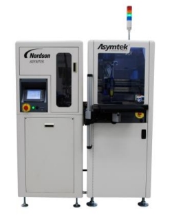
March 3, 2011 — Nordson ASYMTEK, dispensing, coating, and jetting technologies provider, introduced jet dispensing for manufacturing of side-view LEDs. The Spectrum S-920N fluid dispenser jets 0.1 to 0.2mm dots through windows as small as 0.4mm into LED cavities.

Click to EnlargeNordson ASYMTEK’s Spectrum S-920N jetting system automatically maintains a consistent shot weight with software-managed dispense parameters. Closed-loop dispensing eliminates operator adjustment. "Consistent dispensing weight improves process capability while ensuring higher units per hour," said Akira Morita, business development manager at Nordson ASYMTEK. "Using CPJ+ (calibrated process jetting plus), the process variability is reduced for tight LED color quality."

The system uses a jet for non-contact dispensing. Unlike a needle, the jet retracts much less for silicone break off and therefore shoots multiple shots faster, increasing speed and throughput. The jet’s small, controlled drops of fluid reach tight cavities consistently and reliably, unlike needles which have orifices larger than the cavity windows of side-view LEDs. Nordson ASYMTEK states that the system is easier to set up and maintain in production than multi-headed needle dispensing systems.

Side-view LEDs are incorporated into displays in tablet computers, smart phones, e-readers, and other devices. "As these LED devices get slimmer, the challenge to dispense specialized fluids, like silicone phosphor, into these tight spaces becomes greater," explained Morita.

View the free, on-demand webcast, "Light and Color Measurement of Today’s LED Technology" from Konica Minolta here.

Visit Nordson ASYMTEK at SEMICON China Booth 2437.

Nordson ASYMTEK provides precision automated fluid dispensing, conformal coating, and jetting technologies and designs and manufactures a full line of dispensing and coating systems. Nordson Corporation (Nasdaq: NDSN) is one of the world’s leading producers of precision dispensing equipment that applies adhesives, sealants, liquid and powder coatings and other materials to a broad range of consumer and industrial products during manufacturing operations. For more information, visit www.nordsonasymtek.com

Subscribe to Solid State Technology/Advanced Packaging.

Follow Advanced Packaging on Twitter.com by clicking www.twitter.com/advpackaging. Or join our Facebook group

March 2, 2011 — A solid composite heat-conducting material created by Georgia Tech Research Institute (GTRI) scientists has a thermal conductivity that is higher than any metal and takes advantage of the properties of diamond, which is the most thermally conductive material at 2000W m-1 K-1.

Single-crystal diamonds are sometimes used as heat spreaders for semiconductor lasers. The silver-diamond composite is being aimed at cooling wide-bandgap semiconductors planned for next-generation phased-array radars.

The material is made of very small particles of diamond in a matrix of silver. Unlike single-crystal diamond, the small particles are relatively inexpensive. The silver, which is conductive at 400W m-1 K-1, bonds the loose diamond particles into a stable matrix, allows precise cutting of the material to form components of exact sizes, and creates a thermally effective interface between the diamonds.

One of the most important qualities of the silver-diamond composite is that its coefficient of thermal expansion (CTE) can be tailored to match the semiconductor that is being cooled. Otherwise, the heat-conducting layer would delaminate from the semiconductor as temperature changes.

The researchers want to use the composite as a thermal shim with 250µm or thinner thicknesses. Some versions of the composite are up to 85% diamond. The thermal shims made so far are very small, making in-depth testing (which would help to explain the material’s performance in terms of materials science rather than just in terms of performance results) difficult; the GTRI group is evaluating several testbed technologies that hold promise for detailed thermal-conductivity analysis.

February 28, 2011 — The new gold/tin (AuSn) process from Stellar Industries is ideally matched to Stellar’s proprietary CPU copper on aluminum nitride (AlN) submounts with its sharp guillotine edge for precise edge alignments.

Click to EnlargeThe new gold/tin process improves wettability and offers variable freeze time options to ensure efficient laser die bonding. Reduced micro-voiding improves thermal performance for increased reliability.

The AuSn performance is available from 70Au/30Sn to 80Au/20Sn compositions.

Learn more about this product at (508) 865-1668; [email protected]

Subscribe to Solid State Technology/Advanced Packaging.

Follow Advanced Packaging on Twitter.com by clicking www.twitter.com/advpackaging. Or join our Facebook group

February 28, 2011 — Various industries — such as aerospace, sporting goods manufacturers, construction – are incorporating technological advances using nanocomposites, with extraordinary results. Epoxy materials are being transformed into stiffer, lighter, and stronger materials thanks to the addition of fullerenes and carbon nanotubes (CNTs). Dongsheng Mao, Applied Nanotech, Applied Nanotech Holdings (APNT), describes a process involving multi-walled carbon nanotubes (MWCNTs) that have stronger mechanical properties yet remain lightweight and within end-product cost parameters.

These epoxy materials frequently appear in industry as fiber reinforced plastics (FRP). The properties of these new epoxy/carbon nanotube composites are generally not easily transferred to the FRP. However, using this new composite, APNT achieved a 31% improvement in the flexural strength of the final FRP and similar improvements are expected in compression strength.

Click to Enlarge
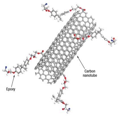
Figure 1. Schematic diagram of carbon nanotube (CNT) reinforced epoxy. Strong bonding between functionalized carbon nanotubes and epoxy is formed to significantly improve mechanical properties of the composites.

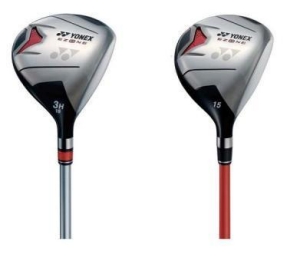
The epoxy/CNT nanocomposite material has properties tailored to 3D assembling, thanks to an ability to uniquely handle blocks of CNTs. Large-volume applications include golf club shaft and sports racquet manufacture. Manufacturers using this material can decrease product weight while maintaining strength, portability, and flexibility. Sporting goods products are only the first application area.

The role carbon nanotubes play

Only 1-2% of the product is carbon nanotubes, yet they improve mechanical properties. By dispersing and functionalizing CNTs individually, ANI spread the CNTs throughout an epoxy matrix such that, when force is applied on the final product, a part of that stress is transferred to the CNTs.

CNTs possess unique mechanical properties. Their stiffness, strength and resilience exceed similar properties of any current material, with the potential for fundamentally new material systems, in particular, structural nanocomposites. Unfortunately, their integration with polymer matrices presents new technical challenges.

CNTs tend to aggregate with each other to form ropes or bundles due to intrinsic van der Waals forces associated with their high surface energy. De-agglomeration and dispersion of CNTs in various media has been recognized as one of the major challenges of commercial CNT adoption. Traditional methods such as sonication, high-shear mixing, stirring, and surfactants are often used in lab-scale quantities to disperse CNTs, but those methods have proven ineffective on an industrial scale. Although surface functionalization of CNTs has improved dispersions, the results for the mechanical properties of CNT-reinforced nanocomposites also depend on mixing procedures and carbon fiber-reinforced polymer (CFRP) manufacture methods.

Transferring interesting and unique nanocomposite properties to CFRPs can be realized only by successfully integrating functionalized CNTs into more complex structures. Using CNTs as a reinforcing component in polymer composites requires the ability to tailor the nature of the CNT walls to control the interfacial interactions between the CNTs and the polymer chains.

Applied’s CNT achieved over 40% improvement in both flexural and compression strength for epoxy/carbon nanotube composites. Chemical and mechanical modification and CNT functionalization, for them to be accepted and integrated properly into the epoxy matrix, were essential.

Click to Enlarge
Figure 2. Yonex’s new golf clubs (EZONE) are made using Applied Nanotech, Inc’s patented technology (www.yonex.co.jp).

Commercializing new CNT products

At times, companies worry about sharing propriety research information. Without all of the pertinent data, it is difficult to clearly understand how to apply nanotechnology methods to achieve the desired result. In cases like this, if the CNTs are not functionalized properly, or epoxy penetration into the fiber is suboptimal, the final material will have visible defects and no mechanical enhancement. Communication between industry and research entities is therefore essential to develop commercially viable products, as APNT demonstrates with this sporting goods partner.

Cost is always a manufacturing consideration. Even the greatest design improvements fail in the market if consumer cost is prohibitive. We advise clients to carefully examine how nanotechnology is applied to a project. In the past, single-wall nanotubes (SWCNTs) have enabled some great results, but costs were exorbitant. Today, functionalized CNT prices are dropping considerably, so we focused on MWCNTs. The results were significantly improved compression strength, flexural strength, modulus, impact strength, and vibration damping factor compared with epoxy.

We have demonstrated that the functionalization and dispersion methods used in CNT-reinforced epoxy and other thermosetting nanocomposites is a promising technology that can be expanded into many other fields, including aviation, defense, aerospace, marine, and cleantech.

Dongsheng Mao received his Ph.D from Chinese Academy of Sciences with a background of Materials Science and Engineering and is director of the Nanocomposite Division at Applied Nanotech. Inc., Applied Nanotech Holdings (Stock Symbol: APNT), 3006 Longhorn Blvd., Suite 107, Austin, TX 78758; [email protected]. Dongsheng Mao is director of Applied Nanotech Inc.’s Nanocomposite Division.

Follow Small Times on Twitter.com by clicking www.twitter.com/smalltimes. Or join our Facebook group
February 25, 2011 – Global production value of nanocarbon products — single-walled carbon nanotubes (SWNT), multi-walled carbon nanotubes (MWNT), fullerenes, graphene, carbon nanofiber, and nanodiamonds — will triple over the next four years in value, and by orders-of-magnitude in actual production, according to a recent analyst report.

Production of carbon nano products totaled about 710 tons in 2010, for a rough value of $435M, calculates Innovative Research and Products Inc. (iRAP). The company predicts that will swell to 9,300t and $1.3B by 2015.


2010
2015
AAGR %
(2010-2015)
SWNT 180 320 12.2
MWNT 105 700 46.7
Fullerenes 61 60 -0.33
CNF 88 144 10
Graphene 0.75 48 130
TOTAL
435
1272
24

Nanocarbon production value (in US $M) according to types. (Source: iRAP)

Inside the numbers, iRap finds some key trends:

  • Production closing the capacity gap. Those surging output numbers for nanocarbon products suggest partially solving a more important problem: massive overcapacity. In 2010, production capacity for these materials was 4065t — actual output of 710t translates to 17% capacity utilization. (Output was only about 500t in 2009, and 340t in 2008.) But by 2015, iRap sees this gulf closing, with actual production doubling over the period to exceed 9300t (a 67.3% annual growth rate), translating to an 80% utilization based on the 12,300t of projected capacity.
  • Despite surging output and capacity, demand hasn’t really caught up yet, iRap notes, but suppliers want to be ready to match future demand seen coming in the next 5-10 years. Contributing to that demand spark, overall prices are coming down: the firm projects prices for all nanocarbon products will fall by an average of ~12%/year from 2010-2015.

  • Nanotubes leading the way. Multiwalled carbon nanotubes (MWNT) will pace the growth, says iRap: 390t of global capacity in 2008, 1500t in 2009, >3400t in 2010, and 9400t by 2015. But single-walled carbon nanotubes (SWNT), the most expensive of the lot, are the key to the kingdom; they "are much more difficult to produce than MWCNTs," iRap notes, and are seen replacing silicon as the ubiquitous electronic starting material within the next decade or so.
  • Asia is production home. Asia’s production capacity for both types of nanotubes (SWNT and MWNT) is 2×-3× higher than North America and Europe combined, says iRap. Japan is a leader in MWNT production (driven by demand for lithium-ion battery electrodes) but China and Korea are catching up fast.

  • Share of nanocarbon production value according to types, 2015 vs. 2010. (Source: iRAP)