Category Archives: Materials and Equipment

February 25, 2011 – Global production value of nanocarbon products — single-walled carbon nanotubes (SWNT), multi-walled carbon nanotubes (MWNT), fullerenes, graphene, carbon nanofiber, and nanodiamonds — will triple over the next four years in value, and by orders-of-magnitude in actual production, according to a recent analyst report.

Production of carbon nano products totaled about 710 tons in 2010, for a rough value of $435M, calculates Innovative Research and Products Inc. (iRAP). The company predicts that will swell to 9,300t and $1.3B by 2015.


2010
2015
AAGR %
(2010-2015)
SWNT 180 320 12.2
MWNT 105 700 46.7
Fullerenes 61 60 -0.33
CNF 88 144 10
Graphene 0.75 48 130
TOTAL
435
1272
24

Nanocarbon production value (in US $M) according to types. (Source: iRAP)

Inside the numbers, iRap finds some key trends:

  • Production closing the capacity gap. Those surging output numbers for nanocarbon products suggest partially solving a more important problem: massive overcapacity. In 2010, production capacity for these materials was 4065t — actual output of 710t translates to 17% capacity utilization. (Output was only about 500t in 2009, and 340t in 2008.) But by 2015, iRap sees this gulf closing, with actual production doubling over the period to exceed 9300t (a 67.3% annual growth rate), translating to an 80% utilization based on the 12,300t of projected capacity.
  • Despite surging output and capacity, demand hasn’t really caught up yet, iRap notes, but suppliers want to be ready to match future demand seen coming in the next 5-10 years. Contributing to that demand spark, overall prices are coming down: the firm projects prices for all nanocarbon products will fall by an average of ~12%/year from 2010-2015.

  • Nanotubes leading the way. Multiwalled carbon nanotubes (MWNT) will pace the growth, says iRap: 390t of global capacity in 2008, 1500t in 2009, >3400t in 2010, and 9400t by 2015. But single-walled carbon nanotubes (SWNT), the most expensive of the lot, are the key to the kingdom; they "are much more difficult to produce than MWCNTs," iRap notes, and are seen replacing silicon as the ubiquitous electronic starting material within the next decade or so.
  • Asia is production home. Asia’s production capacity for both types of nanotubes (SWNT and MWNT) is 2×-3× higher than North America and Europe combined, says iRap. Japan is a leader in MWNT production (driven by demand for lithium-ion battery electrodes) but China and Korea are catching up fast.

  • Share of nanocarbon production value according to types, 2015 vs. 2010. (Source: iRAP)


February 24, 2011 — Multitest, a designer and manufacturer of final test handlers, contactors and load boards used by integrated device manufacturers (IDMs) and final test subcontractors, received its fifth full purchase order for its InCarrier device transfer system with InStrip test handling system adapted to metal frame-based carriers.

This new test handling process differs from traditional tube or tray loading of devices into gravity feed and pick-and-place systems. Instead, singulated devices are loaded into a patented micro-spring carrier frame that is handled on Multitest’s strip handling system.

With the InCarrier device transfer system, Multitest can achieve high test parallelism for singulated devices without compromising quality through post test singulation processing. The actual test handling is practically jam free, even for devices as small as QFN 2 x 2mm.

Multitest manufactures test equipment for semiconductors. Multitest markets test handlers, contactors, and ATE printed circuit boards. For more information about Multitest’s InCarrier, visit www.multitest.com/InCarrier.

Subscribe to Solid State Technology/Advanced Packaging.

Follow Advanced Packaging on Twitter.com by clicking www.twitter.com/advpackaging. Or join our Facebook group

February 24, 2011 — A lab at Rice University has developed an efficient method to disperse nanotubes in a way that preserves their unique properties and adds more. The technique allows inorganic metal complexes with different functionalities to remain in close contact with single-walled carbon nanotubes (SWCNT) while keeping them separated in a solution.

That separation is critical to manufacturers who want to spin fiber from nanotubes, or mix them into composite materials for strength or to take advantage of their electrical properties. The ability to functionalize the nanotubes at the same time may advance imaging sensors, catalysis and solar-activated hydrogen fuel cells.

A batch of nanotubes can stay dispersed in water for weeks on end. Keeping carbon nanotubes from clumping in aqueous solutions and combining them with molecules that add novel abilities have been difficult for scientists exploring the use of these highly versatile materials. They’ve tried attaching organic molecules to the nanotubes’ surfaces to add functionality as well as solubility. But while these techniques can separate nanotubes from one another, they take a toll on the nanotubes’ electronic, thermal and mechanical properties.

Angel Marti, a Rice assistant professor of chemistry and bioengineering and a Norman Hackerman-Welch Young Investigator, and his students reported this month in the Royal Society of Chemistry journal Chemical Communications that ruthenium polypyridyl complexes are highly effective at dispersing nanotubes in water efficiently and for long periods. Ruthenium is a rare metallic element.

Marti and his team created ruthenium complexes by combining the element with ligands, stable molecules that bind to metal ions. The resulting molecular complex is part hydrophobic (the ligands) and part hydrophilic (the ruthenium). The ligands strongly bind to nanotubes while the attached ruthenium molecules interact with water to maintain the tubes in solution and keep them apart from one another.

Another key turned out to be moderation. Marti and co-authors Disha Jain and Avishek Saha — Jain is a former postdoctoral researcher in Marti’s lab, and Saha is a graduate student — were originally eyeing ruthenium complexes as part of a study to track amyloid deposits associated with Alzheimer’s disease. "We started to wonder what would happen if we modified the metal complex so it could bind to a nanotube," Marti said. "That would provide solubility, individualization, dispersion and functionality."

"Avishek put this together with purified single-walled carbon nanotubes (created via Rice’s HiPco process) and sonicated. Absolutely nothing happened. The nanotubes didn’t get into solution — they just clumped at the bottom.

"That was very weird, but that’s how science works — some things you think are good ideas never work."

Saha removed the liquid and left the clumped nanotubes at the bottom of the centrifuge tube. "So I said, ‘Well, why don’t you do something crazy. Just add water to that, and with the little bit of ruthenium that might remain there, try to do the reaction.’ He did that, and the solution turned black."

A low concentration of ruthenium did the trick. "We found out that 0.05% of the ruthenium complex is the optimum concentration to dissolve nanotubes," Marti said. Further experimentation showed that simple ruthenium complexes alone did not work. The molecule requires its hydrophobic ligand tail, which seeks to minimize its exposure to water by binding with nanotubes. "That’s the same thing nanotubes want to do, so it’s a favorable relationship," he said.

Marti also found the nanotubes’ natural fluorescence unaffected by the ruthenium complexes. "Even though they’ve been purified, which can introduce defects, they still exhibit very good fluorescence," he said.

He said that certain ruthenium complexes have the ability to stay in an excited state for a long time — about 600 nanoseconds, or 100 times longer than normal organic molecules. "It means the probability that it will transfer an electron is high. That’s convenient for energy transfer applications, which are important for imaging," he said.

That nanotubes stay suspended for a long time should catch the eye of manufacturers who use them in bulk. "They should stay separated for weeks without problems," Marti said. "We have solutions that have been sitting for months without any signs of crashing."

The Welch Foundation supported the research.

More information can be found at www.rice.edu

Follow Small Times on Twitter.com by clicking www.twitter.com/smalltimes. Or join our Facebook group

February 24, 2011 – GLOBE NEWSWIRE — FEI (Nasdaq:FEIC) and CEA-Leti entered into a three year agreement to characterize advanced semiconductor materials for the 22nm technology node and beyond. European-based CEA-Leti, with its two partners on the NanoCharacterization Platform of MINATEC Campus, CEA-Liten (new materials for new energies) and CEA-INAC (Nanoscience Institute), will apply their expertise in holography and nanobeam diffraction. FEI will provide advanced nanobeam diffraction technology with its Titan scanning transmission electron microscope (S/TEM). The companies will measure strain changes in semiconductor structures.

"The research will focus on two important areas: use of holography with the Titan’s unique XFEG electron source to improve the sensitivity of dopant profiling, and the use of nanobeam diffraction techniques to measure changes in strain and other crystallographic parameters," said George Scholes, vice president and general manager for FEI’s S/TEM product line.

"We must improve the sensitivity, accuracy and throughput of dopant profiling in order to continue supporting shrinking device dimensions. And a better understanding of the effects of strain is critical in the development of higher performance IC devices as we continue to push the technology to the 22nm technology node and beyond," stated Rudy Kellner, vice president and general manager of FEI’s Electronics Division.

According to Laurent Malier, CEO of CEA-Leti, FEI offers a powerful, widely available microscope as well as expertise in nanobeam diffraction applications.

For more information, visit http://www.fei.com or www.leti.fr.

CEA is a French research and technology organization, with activities in four main areas: energy, information technologies, healthcare technologies and defence and security. Within CEA, the Laboratory for Electronics & Information Technology (CEA-Leti) works with companies in order to increase their competitiveness through technological innovation and transfers. CEA-Leti is focused on micro and nanotechnologies and their applications, from wireless devices and systems, to biology and healthcare or photonics. Nanoelectronics and microsystems (MEMS) are at the core of its activities.

FEI (Nasdaq:FEIC) is a diversified scientific instruments company. It is a premier provider of electron- and ion-beam microscopes and tools for nanoscale applications across many industries: industrial and academic materials research, life sciences, semiconductors, data storage, natural resources and more.

Subscribe to Solid State Technology/Advanced Packaging.

Follow Solid State Technology on Twitter.com via editors Pete Singer, twitter.com/PetesTweetsPW and Debra Vogler, twitter.com/dvogler_PV_semi.

Or join our Facebook group

February 24, 2011 – FARS News Agency — Iranian researchers at Kashan University calculated the physical and mechanical properties of multi-walled carbon nanotubes (MWCNT) and nitride-Bohr nanotubes in a move to help improve the design of arms for nano-robots.

The body of the nano robot has joints or fixed points around which arms move. This research studies the various stability types of two-walled or multi-walled carbon nanotubes in an elastic environment around these moving parts. "What distinguishes this study from all other researches carried out recently is the presentation of Pasternak model that considers the effect of shear forces applied by the elastic environment to the two-walled carbon nanotubes," Dr. Ali Qorbanpour Arani, a lecturer at University of Kashan, told the Iran Nanotechnology Initiative Council.

Arani, a member of the Nanoscience and Nanotechnology Research Center of University of Kashan added, "In this study, the physical and mechanical properties of the multi-walled carbon and nitride-Bohr nanotubes were determined. The properties can be used in the design of nano-robots’ arms. In addition, they can be used as intelligent nanotubes due to their piezoelectric properties by using electrical field on them, and they can control the rotation and movement or the kinetic of the movement in the arms and neck of the nano-robot."

"Taking into account the fact that nanotubes are usually studied in an elastic environment, in order to calculate the forces applied to nanotubes, which include vertical and shear forces, we used Winkler model (for studying the vertical forces) and Pasternak model (for the vertical and shear forces) to obtain more precise results," Qorbanpour Arani concluded.

Copyright 2011 Fars News Agency. All Rights Reserved

Follow Small Times on Twitter.com by clicking www.twitter.com/smalltimes. Or join our Facebook group

February 24, 2011 — Custom fabricated sapphire wafer carriers that are uniform, parallel, and impervious to solvents and etchants for thinning semiconductor materials are available from Meller Optics Inc.

Meller Sapphire Wafer Carriers feature ±1.2µm thickness and part-to-part uniformity, with parallelism to 10arc-sec., depending upon size, and exhibit Moh 9 hardness, second only to diamond. They are suited to thinning semiconductor materials such as GaAs, available plain or perforated with custom patterns for hold-down or delamination.

Impervious to solvents, etchants, and capable of withstanding repeated use, Meller Sapphire Wafer Carriers are chip-, chemical-, and scratch-resistant.  Custom fabricated in 2" to 6" diameter sizes as thin as 0.018", they can be supplied with flats, laser markings, and other special characteristics.

For more information, visit www.melleroptics.com

Subscribe to Solid State Technology/Advanced Packaging.

Follow Solid State Technology on Twitter.com via editors Pete Singer, twitter.com/PetesTweetsPW and Debra Vogler, twitter.com/dvogler_PV_semi.

Or join our Facebook group

February 23, 2011 – More evidence for a slowing market: SEMI’s January data is back on a downward trend for demand in semiconductor equipment, though the group is "encouraged" by recent capex announcements.

A look inside the January 2011 numbers:

  • After December’s 4% snapback, bookings are headed back down the slope again, -3% M/M to $1.53B. That’s five declines in the past six months, eroding more than $300M or about 16%. (And the massive Y/Y comparisons we’ve enjoyed the past year? Gone. It’s now just 30%, less than half the Y/Y growth in December 2010.)
  • Billings fell back off a December surge to a small 2.5% increase to $1.80B. They’re still double the level they were at a year ago, and now back above mid-2007 levels. (Next stop: early-2001 levels?)
  • The book-to-bill ratio fell again in January to 0.85, which translates to $85 worth of orders received for every $100 billed. That’s a trend of less business coming in than going out. And we’re now four months below the 1.0 parity mark, a consecutive stretch not seen since the spring of 2009 — but that’s when numbers were rising off the bottom of the downturn. A four-month stretch of increasingly sub-parity B:B hasn’t been seen since early 2008.

SEMI backdated about $55M in tool sales and an extra ~$45M in orders to its December figures, but those didn’t change the B:B.

Despite the direction of tool orders, SEMI president/CEO Stanley Myers noted in a statement that industry spending is still solid, and he is "encouraged by the strength in capital expenditure plans announced over the past month."

Click to Enlarge
North American equipment demand in US $M, a 3-mo. average. (Source: SEMI)

In Japan, the trend of slowing demand was similar. Semiconductor tool sales rebounded about 5% after a December lull (+66% vs. a year ago) to ¥103.96B (US $1.24B), but orders slipped about -3% M/M (+21.5% Y/Y) to ¥103.36B ($1.24B), pushing the B:B ratio just below the parity level at 0.99. It’s the first sub-parity B:B in Japan in nearly two years, since May 2009, according to SEAJ data. Bookings levels have pulled back almost 20% since their September peak; billings are off about -7%.

Click to Enlarge

By Debra Vogler, senior technical editor

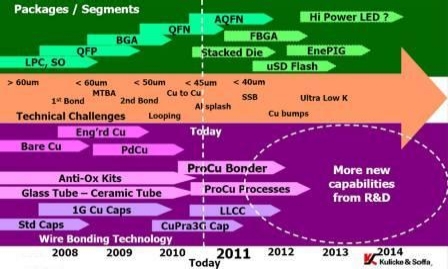
February 23, 2011 — As gold becomes more expensive, copper wire bonding becomes more appealing for chip packaging. Reverse bonding, fine-pitch bonding, looping, second bonds, and other technologies are ramping on roadmaps, according to Kulicke & Soffa (K&S).

Bob Chylak, VP engineering, packaging & process integration at Kulicke & Soffa, was the featured speaker at a recent iMAPS NorCal chapter lunch meeting (Santa Clara, CA; 2/2/11). He covered the topic of converting from gold to copper for wire bonding — a move gaining ever greater interest by the surging price of gold. With heightened activities to close the knowledge gap with respect to using copper, many of the challenges have been addressed, observed Chylak.

Listen to Chylak’s interview:  Download (iPhone/iPod users) or Play Now

Laying out his company’s copper R&D roadmap (figure), Chylak noted that high-volume production of fine-pitch copper replacing gold already started in 2010. Advanced QFNs and stacked die still need to be developed, and LED packaging needs to be transitioned to copper, though Chylak noted that the challenge there will be with copper’s reflectivity not being as good as gold.

Click to Enlarge

Figure. Copper transition and roadmap planning. SOURCE: Kulicke & Soffa

Chylak said that nearly the entire K&S process engineering staff is working on the copper transition. In particular, work is being done on reverse bonding and getting yields to 50ppm or less. "It’s mainly around the looping [for stacked dies] and second bonds [including for LEDs] we’re focusing on," said Chylak.

Subscribe to Solid State Technology/Advanced Packaging.

Follow Advanced Packaging on Twitter.com by clicking www.twitter.com/advpackaging. Or join our Facebook group

February 22, 2011 — CEA-Leti, in a multi-partner project with SET, STMicroelectronics, ALES and CNRS-CEMES, will demonstrate high-alignment-accuracy (<1µm) chip-to-wafer structures made by direct metallic bonding. Such structures are required for high-performance 3D integrated circuits and could enable a wide range of applications in microelectronics as well as in optoelectronics or MEMS.

The chip-to-wafer direct-metallic-bonding technology was developed at Leti to break through certain 3D-integration limitations. For example, the technology allows chips to be attached to a substrate at low temperature and with low bonding pressure. This technology also allows interconnecting the chip and the substrate electrically through local metallic bonding.

Leti has acquired a customized 300mm FC300 pick-and-place tool from SET, Smart Equipment Technology, to demonstrate the technology. The equipment was developed by SET based on its high placement accuracy FC300 system to adapt it to direct-metallic-bonding requirements.

The customized system will be used by the Minalogic PROCEED project. Minalogic is a global competitive cluster specialized in micro- and nanotechnologies and embedded intelligence. In addition to Leti and SET, partners are STMicroelectronics, ALES and the CNRS-CEMES. The PROCEED Minalogic project is a EUR4.2 million, 24-month project that began in December 2009 and is supported by French FIU (Fond Interministeriel Unique).

"SET has a strong interest for this non-thermocompression metal-to-metal bonding, which may be a key to throughput improvement required for the adoption of 3D-IC integration," said Gaël Schmidt, managing director of SET.

CEA is a French research and technology organization, with activities in four main areas: energy, information technologies, healthcare technologies and defence and security. Within CEA, the Laboratory for Electronics & Information Technology (CEA-Leti) works with companies in order to increase their competitiveness through technological innovation and transfers. CEA-Leti is focused on micro and nanotechnologies and their applications, from wireless devices and systems, to biology and healthcare or photonics. Nanoelectronics and microsystems (MEMS) are at the core of its activities. Visit www.leti.fr.

SET, Smart Equipment Technology, is a supplier of high-accuracy die-to-die, die-to-wafer bonding and nanoimprint lithography products. SET is a wholly owned subsidiary of Replisaurus Technologies. Further information is available on www.set-sas.fr.

Subscribe to Solid State Technology/Advanced Packaging.

Follow Advanced Packaging on Twitter.com by clicking www.twitter.com/advpackaging. Or join our Facebook group

By Debra Vogler, senior technical editor

February 18, 2011 — Jamal Izadian, co-founder & president of RFCONNEXT, made the case for shaped membrane transmission lines (SMTL) for use in high-speed 3D packaging applications, as guest speaker at a recent MEPTEC lunch forum (2/9/11, Santa Clara, CA). Observing that wire bonding is limiting high-speed performance and die stacking, and that high-speed digital signals are limited by traditional plastic packaging, he calls for SMTL use, in conjunction with two other solutions, called periodic micro transmission lines (PMTL) and via micro transmission lines (VMTL), as a total high-speed packaging interconnect solution.

Listen to Izadian speak: Download (iPhone/iPod users) or Play Now

Each of these technologies is described in a podcast interview with Izadian. He also explains how SMTL supports and improves flip-chip, micro-bumping, wafer thinning, system-in-package (SiP), package-on-package (PoP), and other packaging processes by extending the bandwidth and high-speed limits of these technologies.

An intriguing topic covered in the interview is Izadian’s contention that SMTL is an inexpensive PCB alternative solution to TSVs. Wire bonds are not transmission lines, so high-speed connectivity is not possible, observed Izadian. “With the advent of advanced transmission lines, which are almost as good as a coaxial line at the microscopic level, we have removed the requirement for the connections to be next to each other or on top of each other,” said Izadian. “You can have them dispersed around like a SiP and be able to connect them at high speed.” SMTL technology also allows plastic packaging to be used for high-speed applications, essentially obtaining the performance achieved with ceramic packages, but at a lower cost.  

Some of the advantages of SMTL include: controlled impedance, no parasitic inductance, no significant length limit, no cross-talk, noise immunity, 90% less metal in the process, and scalability.
 
SMTL for packaging applications is currently under evaluation by end users and RFCONNEXT intends to adapt the technology to existing manufacturing processes. Izadian said he expects advanced transmission lines to be ready within the next 6-12 months. Learn more at http://www.rfconnext.com/

Subscribe to Solid State Technology/Advanced Packaging.

Follow Advanced Packaging on Twitter.com by clicking www.twitter.com/advpackaging. Or join our Facebook group