Category Archives: Test and Measurement

WILFRIED VOGEL*, NETA, Talence, France

*No longer at NETA; Please contact CEO Julien Michelon, [email protected] for any inquiries.

Downsizing and thinning all the electronic parts has always been a trend in our modern era. However, the nanoscience and nanotechnologies were still science fiction in the ‘60s and the word nanotechnology was used for the first time in 1974. At the same time, the first atomic force microscopes (AFM) and scanning acoustic microscopes (SAM) were developed. Today nanotechnologies represent huge investments –  even from governments – and a global market of several thousand of billions of euros.

Non-destructive testing at the nanometric scale is the purpose here. Ultrasounds are widely used in the aeronautics industry or during medical echography. The spatial resolution reached in that case is around the millimeter which is a million time too large when we speak of nanotechnologies.

SAM systems benefit from a higher definition thanks to MHz/GHz ultrasounds, the smallest axial resolution found on the market is below the micron.

The nanometric world requires another 2 to 3 orders of magnitude below and it can only be reached thanks to THz ultrasounds. These frequencies cannot be generated with standard transductors, that’s why the ASynchronous OPtical Sampling (ASOPS) systems are equipped with ultrafast lasers.

This complex technology is now available on the market in a compact instrument. The JAX is the first industrial imaging ASOPS system (FIGURE 1).

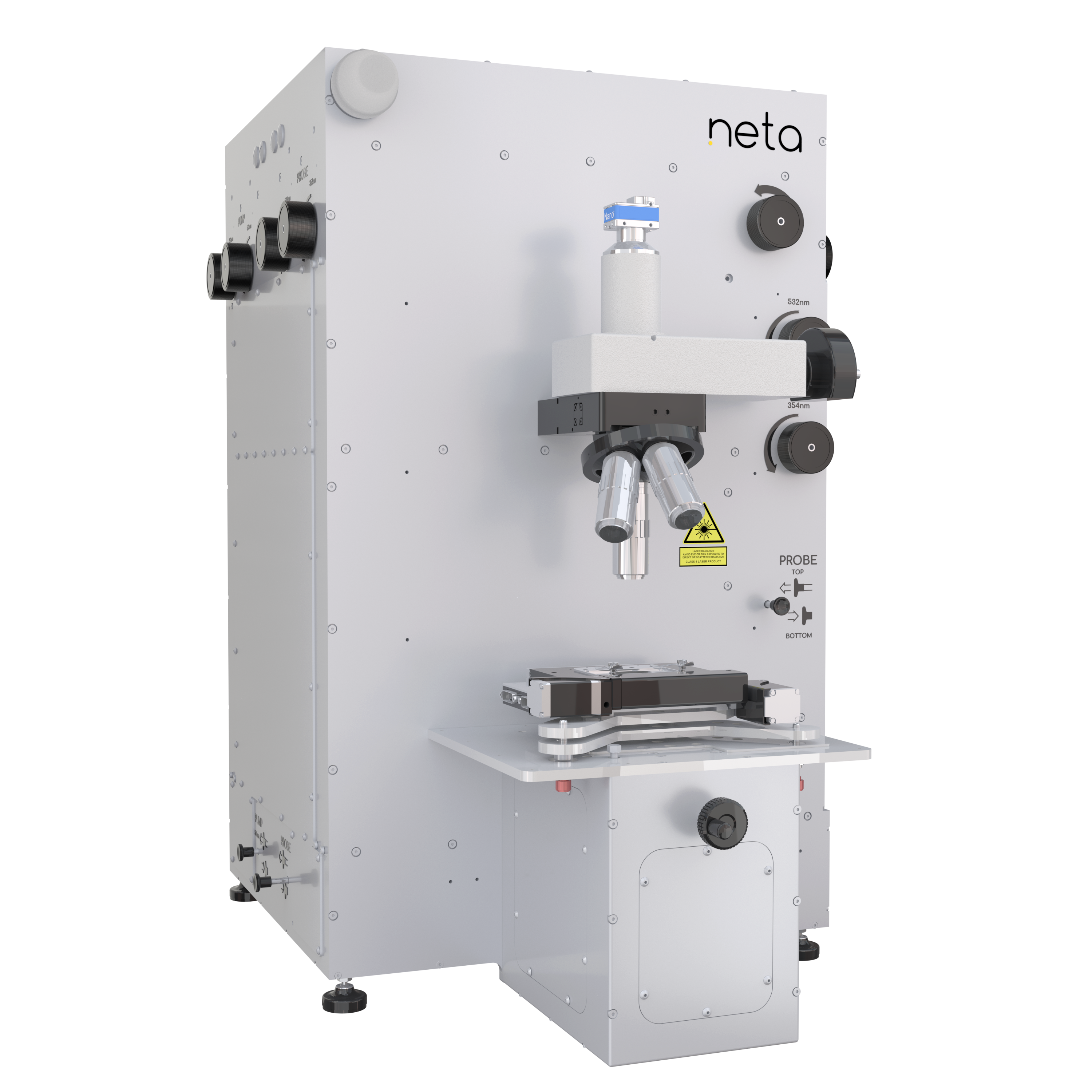
FIGURE 1. JAX imaging system.

When the laser hits the surface, the most part of the energy is absorbed by the first layers of atoms and converted into heat without damaging the sample (FIGURE 2), leading to transient thermoelastic expansion and ultrasound emission. The choice of the probe is also important to keep the temporal and the spatial resolution as low as possible, that’s why another ultrafast laser is used as a probe (FIGURE 3).

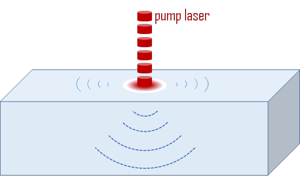
FIGURE 2. ASOPS principle: ultrasound generation.

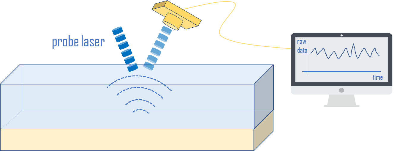
FIGURE 3. ASOPS principle: ultrasound detection.

The ultrasound is propagating a few nanometers per picosecond through the thin film and at some point will bounce back partially or completely to come back to the surface when meeting a different medium.

The probe laser is focused at the surface, when the ultrasound hits back the surface, the reflectivity fluctuates locally over time. The variation of reflectivity is detected and stored into the computer as a raw data. The technique is often called picosecond ultrasonics, it has been developed at Brown University in the USA by Humphrey Maris in the mid 80’s.

The ASOPS is not the only kind of technology able to perform picosecond ultrasonics, but it’s the latest evolution and the fastest to perform a full measurement. The trick here is to slightly shift the frequency of the probe laser compared to the pump’s one (FIGURE 4). Both lasers are synchronized by a separate electronical unit. The probe arrives slightly after the pump and this delay is extending with time until the whole sampling is over.

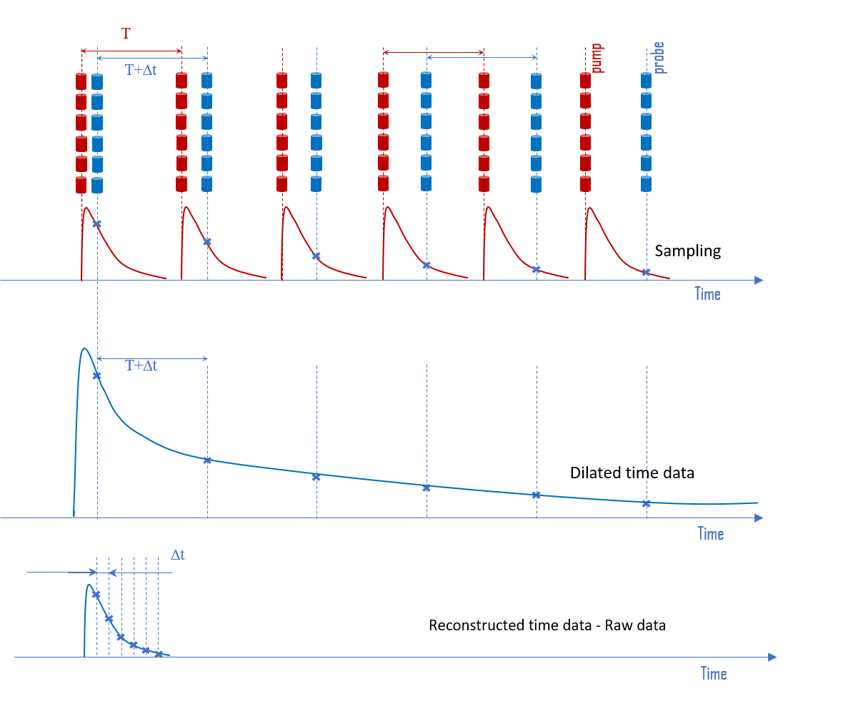
FIGURE 4. Asynchronous pump and probe lasers sampling concept.

The elastic answer of the thin film to a pump excitation is too fast to be measured in real time. You have to artificially extend time and reconstruct the signal of the probe.

The measure described above is for one single point. With a more standard instrument able to perform picosecond ultrasonics, it would take several minutes. Here with the ASOPS, the measure takes less than a second. It means that by simply scanning point by point all over the surface (FIGURE 5), you will get a full map of the studied mechanical parameter in minutes.

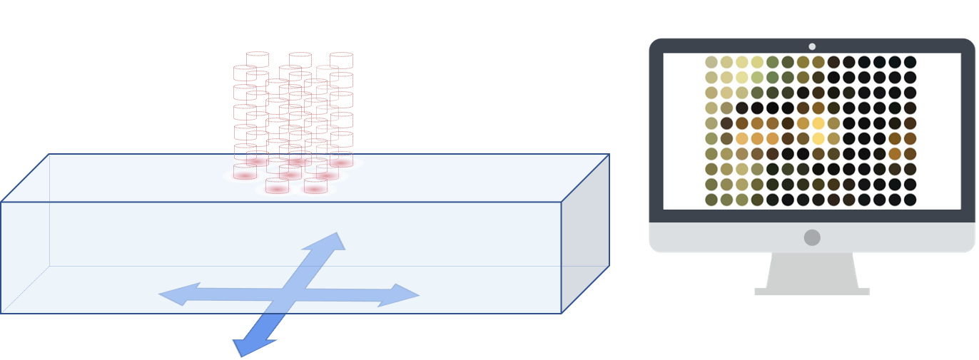
FIGURE 5. Mapping of sample’s thickness.

Thickness measurement

For instance, if your interest is in the thickness of a thin film, you can easily retrieve an accurate value by measuring the time between two echoes of the ultrasound at the surface of the sample (FIGURE 6).

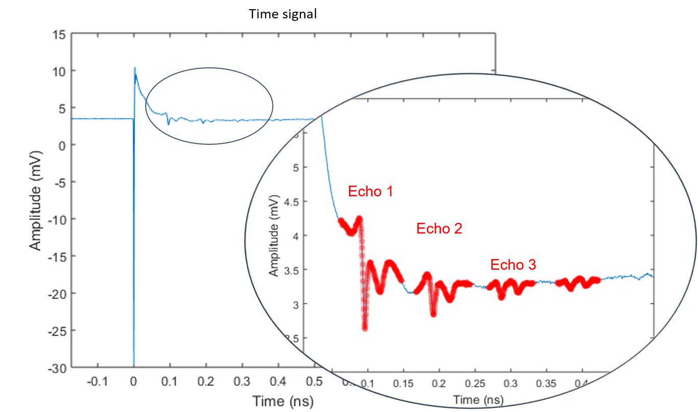
FIGURE 6. Example of raw data.

Until recently, the kind of setup required to make these measurements was found in a optical lab with a large honeycomb table full of mirrors and lenses. Even though the results are respectable, the time to install and repeatability are often the main issue.

Hopefully the technology is now accessible for non-specialists who just want to focus on measuring the mechanical properties of their samples and not to take care of all the optical part. The industrialization of such an innovative and complex device is giving an easy access to new information.

Since a punctual measurement takes a few milliseconds, it is easily feasible to measure all over the surface of the sample and get a full mapping of the thickness.

In the example below (FIGURE 7), the sample consists of a 500 µm silicon substrate and 255 nm sputtered tungsten single layer. The scanned surface is approximately 1.6 mm x 1.6 mm and the lateral resolution in X-Y is 50 µm, 999 points in total.

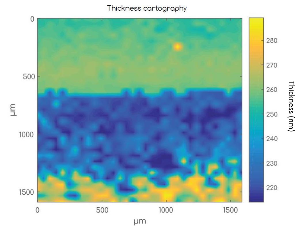
FIGURE 7. Example of sample thickness mapping with ASOPS system.

7b. Microscope view of the sample.

A large scratch is being highlighted at the surface but the average thickness remains in the range of 250 nm. The total time of measurement is less than 10 minutes, which is comparable to a single point measurement with one laser and a mechanical delay line (homodyne system).

Until now, the industry offer for production management was only homodyne instruments performing picosecond ultrasonics measurements, reducing the full scan of the surface to a very few points checked only over a full wafer.

We just saw that single layer thin film thickness measurement is pretty straight forward. If you are dealing with more than one layer the raw data is much more complex to read. However, it is possible to model the sample and to compare the simulated signal to the actual measure with an incredible fit.

Multiphysics

When you chat with several experts of thin films, they will all agree to tell you that:

  • Thickness is a key parameter
  • Adhesion is always a problem
  • Non-destructive measurement is a fine improvement
  • Faster is better
  • Imaging is awesome

In the industry, thickness and adhesion are the main concern at all steps of the manufacturing process, whether you are working in the display or the semiconductor field. The picosecond ultrasonics technique is already used in-line for wafer inspection, which shows its maturity and yet confidentiality.

The standard procedures for adhesion measurement are applicable only on flat and large samples, and they are destructive. When it comes to 3D samples and if you want to check the adhesion on a very small surface, the laser is the only solution. Adhesion can now be verified inline all over the sample during every step of the manufacturing process.

Now the academic world has different concerns and goes deeper and deeper in the understanding of the material behavior at the atomic scale.

The ASOPS system can go beyond the picosecond ultrasonics — which is already a great source of information if we stick to thickness and adhesion — and get even more from the raw data such as thermal information or critical mechanical parameters.

Thermal conductivity

Thermal conductivity is the parameter representing the heat conducting capability of a material.

Thin films, superlattices, graphene, and all related materials are of broad technological interest for applications including transistors, memory, optoelectronic devices, MEMS, photovoltaics  and more. Thermal performance is a key consideration in many of these applications, motivating efforts to measure the thermal conductivity of these films. The thermal conductivity of thin film materials is usually smaller than that of their bulk counterparts, sometimes dramatically so.

Compared to bulk single crystals, many thin films have more impurities which tend to reduce the thermal conductivity. Besides even an atomically perfect thin film is expected to have reduced thermal conductivity due to phonon leakage or related interactions.

Using pulsed lasers is one of the many possibilities to measure the thermal conductivity of a thin material. The time-domain thermoreflectance (TDTR) is a method by which the thermal properties of a material can be measured. It is even more suitable for thin films materials, which have properties that vary greatly when compared to the same materials in bulk.

The temperature increase due to the laser can be written as follows:

where R is the sample reflectivity,

Q is the optical pulse energy,

C is the specific heat per unit volume,

A is the optical spot area,

ζ is the optical absorption length,

z is the distance into the sample

The voltage measured by the photodetector is proportional to the variation of R, it is possible then to deduce the thermal conductivity.

In some configuration, it can be useful to shoot the probe on the bottom of the sample (FIGURE 8) or vice versa in order to get more accurate signal from one side or the other of the sample.

Surface acoustic wave

When the pump laser hits the surface, the ultrasound generated is actually made of two distinct waves modes, one propagating in the bulk, which is called longitudinal (see Fig. 2), one traveling along the surface, it’s called the Rayleigh mode.

In the industry the detection of surface acoustic wave (SAW) is used to detect and characterize cracks.

The surface wave is very sensitive to the presence and characteristics of the surface coatings, even when they are much thinner than the penetration depth of the wave.

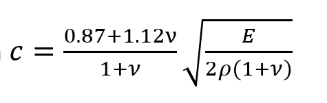
Young’s Modulus can be determined by measuring the velocity of the surface waves.

The propagation velocity of the surface waves, c, in a homogeneous isotropic medium is related to:

  • the Young’s modulus E,
  • the Poisson’s ratio ,
  • the density

by the following approximate relation

When using an industrial ASOPS system to measure and image the SAW, the pump laser is fixed (Fig. 8) and always hitting the same spot. The probe is measuring its signal around the pump laser thanks to a scanner installed in the instrument.

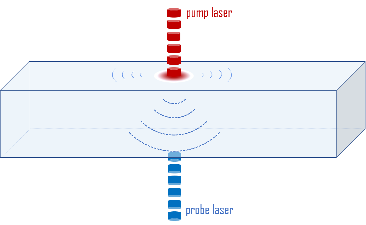
FIGURE 8. ASOPS principle: Top / Bottom configuration.

Future Challenges

Today ASOPS technology is moving from the margin to the mainstream. The academic community already recognizes this non-destructive technology as truly operational and able to deliver reliable and accurate measurements. For industrial applications, ASOPS systems will most certainly begin to replace standard systems in the short term and to fill the gap of ultrasonic inspection at nanometric scale. It is also easily nestable in the production line while some other instruments are meant to remain research devices because they require much more care, vacuum pumps, complex settings etc.

However, the industry is far from done exploiting the full range of capabilities offered by ASOPS systems, this versatile technology also continues to be developed and validated for a broad range of other critical applications. Indeed, ASOPS systems has already shown a great potential on biological cell research. We can expect new developments to be done in the future and see instruments help the early disease detection within the next few years.

WILFRIED VOGEL is a sales engineer for NETA, Talence, France. www.neta-tech.com, [email protected]


By Debra Vogler, SEMI

The demand for smartphones and other portable devices that need efficient power management is driving the analog IC market. Additionally, growth is fueled by the Internet of Things (IoT) and the MEMS/sensors devices that enable it. To explore the supply chain opportunities within the analog sector, including MEMS/sensors, SEMI introduced the Analog and New Frontiers Program at SEMICON West 2016. This program — part of the Extended Supply Chain Forum — will feature four, hour-long sessions, each focusing on a different supply chain challenge or area of interest within the analog sector. One of the featured speakers will be Dr. Peter Hartwell, senior director of Advanced Technology at InvenSense. Dr. Hartwell’s pre-show interview provides a provocative look at supply chain challenges facing MEMS/sensors manufacturers.

Perhaps the most significant challenge facing manufacturers of MEMS/sensors is commoditization of sensors and where the profits end up. “The windfall is going to the people enabling the applications at the top,” Hartwell told SEMI. “Especially with mobile devices and IoT.” He pointed out that if there isn’t a way for value capture at the lowest levels – i.e., the companies that enable the systems and devices that create the IoT experience – he predicts a plateau of innovation. “We won’t have the resources to push technology forward, so as a sensor company, we are trying to find ways to move further up the value chain to extract some of that value.”

Moving up the value chain, however, requires sensor companies to become more aware of system considerations. Design convergence is one way to accomplish this. “We think of design convergence as SiPs (System in Package) or SoCs (System on a Chip),” said Hartwell. “We start to put together our sensors with other capabilities, whether that means having processing power in our package or looking at different kinds of sensors that come together.”

He speculates about a time when there will be a single-chip IoT device, i.e., a one-chip device comprising sensors, storage, radio, power management, and perhaps even energy harvesting. “Maybe that’s where the convergence goes.” Still, in the end, the challenge becomes how the industry gets the money back to the bottom of the supply chain. “We’re inching up towards where that money is by building those systems and understanding what it takes to make them.”

The fabless model for MEMS/sensors

Aside from the commoditization conundrum, Hartwell sees another supply chain opportunity arising if the industry embraces a truly fabless business model. Such a model would be based on companies that only design the devices with the process kits arising from different companies. The fundamental question with that scenario, Hartwell notes, is how the various MEMS/sensors houses differentiate themselves.

Hartwell noted that InvenSense embraces the fabless model — the company has a Shuttle program with its foundry partners, TSMC and GLOBALFOUNDRIES. The InvenSense Shuttle gives MEMS developers the opportunity to fabricate their designs on the patented InvenSense Fabrication MEMS-CMOS integrated platform. Though competitors are not able to take part in the Shuttle program, it is available to universities and start-up partner companies. That said, Hartwell noted that the company keeps its ‘cards pretty close to the vest.’ So the challenge is how to open up that model while retaining differentiation when fabs and foundries tend to want to wring out cost from process development by using as much standardization as possible.

“The million dollar question,” said Hartwell, “is could we ever get to the point where the foundry tells the sensor companies what to do — the EDA companies would love to see this happen because it would lead to standardization of design tools and simulators.”

Opportunities for test and the digital interface

Test and packaging are two more opportunity areas for the supply chain. Hartwell pointed out that most MEMS/sensors companies do their own testing using their own test infrastructure. “It’s one differentiator that we haven’t been willing to give up,” said Hartwell. “So this is an opportunity for someone to come in and turn over the apple cart.”

With the proliferation of sensors that need to interface with a multi-chip system comes the challenge of having to connect using more and more pins. And though the industry has solutions for a digital interface to the sensor world, additional work needs to focus on making that interface robust. Hartwell explained that multiple interrupts and digital lines are needed and it gets complicated when you have five, six, or seven sensors in a system. “There are just not enough pins,” said Hartwell. “So we’re seeing a change in the wiring and the interface will have to be something new to solve the integration problem, which has become nontrivial.” He further observed that IoT is driven by four attributes: size, cost, power, and performance. “To get to the promise of IoT, it will take breakthroughs to get to a trillion sensors. You will have to reduce size, cost, power and performance, and some of those by one or two orders of magnitude.”

Wringing out costs with packaging (or, “no” package)

Hartwell minces no words when it comes to tackling size and cost in MEMS: packaging is MEMS. “This is the biggest opportunity to take out size and cost,” Hartwell told SEMI. “The influence of packaging on the transducer can’t be ignored. Packaging hurts the size, it hurts performance, and it’s something for which I don’t want to pay. It’s a huge opportunity for a shift.”

For Hartwell, the crux of the challenge is how to take a single piece of silicon that has a 6-axis sensor system, and then test it, trim it, ship it, and put it into whatever system it’s going into without changing its trim. While chip-scale packaging could be the opportunity the MEMS industry needs, he wants to keep the options open for other ways to break the paradigm.

What’s clear is that ample business opportunities exist for the supply chain within the MEMS/sensors sector to get rid of cost and size, address the test challenge, get rid of the package, and finally, new ways to handle and assemble parts.

To learn more, attend the Analog and New Frontiers Forum (part of the Extended Supply Chain Forum) at SEMICON West. The forum will be held on Wednesday, July 13, in four, hour-long sessions on the Keynote Stage, North Hall, Moscone Center. Check the SEMICON West 2016 website for more details and a list of confirmed speakers for each of the sessions.

SAN JOSE, Calif. — Nov. 11, 2015 — Ultratech, Inc., a supplier of lithography, laser-processing and inspection systems used to manufacture semiconductor devices and high-brightness LEDs (HB-LEDs), as well as atomic layer deposition (ALD) systems, today introduced the Superfast 4G+  in-line, 3D topography inspection system. Ultratech’s new 4G+ system builds on the field leadership of the Superfast 4G, providing the industry’s highest-productivity and lowest-cost solution for high-volume manufacturing. The Superfast 4G+ system’s patented coherent gradient sensing (CGS) technology enables Ultratech customers to use a single type of wafer inspection tool to measure patterned wafers across the entire fab line at the lowest cost. Ultratech plans to begin shipping the Superfast 4G+ systems in the first quarter of 2016.

Superfast 4G+ features include:

  • Direct, front-side 3D topography measurement for opaque and transparent stacks patterned wafers
  • 150 wph, the highest industry 3D in-line inspection throughput with the smallest footprint
  • 1-mm edge exclusion enabling full-wafer pattern inspection and thin-film 3D process control
  • Large bow option for in-line manufacturing control of highly bowed wafers without impacting throughput

Damon Tsai, Ultratech Asia Director for Inspection Systems, said, “Our current leadership position in in-line 3D inspection at advanced memory and foundry manufacturers with Superfast 4G has provided us with a tremendous learning environment. Our partners have helped us develop new hardware capabilities like the ‘Recipe Driven Range Control,’ an innovative high-throughput, large bow optical option on board the Superfast 4G+, as well as new fleet management performance metrics. The inherently simple design of the CGS technology is enabling us to rapidly deliver new capabilities and performance improvements over more complex optical solutions.”

Based on patented CGS technology, Ultratech’s Superfast 4G+ inspection system provides the industry’s highest throughput (150 wph) with the lowest cost-of-ownership compared to competing systems. The direct, front-side 3D topography measurement capability is well-suited for patterned wafer applications such as lithography feed-forward overlay distortion and edge-defocus control as well as thin-film deposition stress and planarization control. Delivering a 2X improvement in performance with fleet matching TMU (Total Measurement Uncertainty), along with the ability to measure opaque and transparent stacks on patterned wafers, the Superfast 4G+  provides cost-effective technology to address the critical needs of its global customers. In addition, leveraging the same breakthrough CGS optical module, the Superfast 4G+ is available as a field upgrade of the Superfast 4G.

Portland, OR — November 4, 2015 — JEOL‘s new JSM-IT100 is the latest addition to its InTouchScope Series of Scanning Electron Microscopes. Representing 50 years of industry leadership with advances in SEM, the IT100 is a simple-to-use versatile, research-grade SEM with a compact ergonomic design.

JEOL JSM-IT100_20Featuring expanded EDS analysis capabilities and ports for multiple detectors, the InTouchScope is a versatile workhorse SEM that can be configured to meet individual lab requirements at an exceptional value. It offers high resolution imaging and a range of acceleration voltages at both high and low vacuum modes.

The IT100 is a remarkably intuitive, high throughput microscope designed to streamline workflow in any lab. Touchscreen operation, or traditional keyboard and mouse interface are at the operator’s fingertips. Fast data acquisition make imaging and analysis of samples a simple task.

With the IT100, it is simple to quickly obtain high quality images using both Secondary Electron and Backscatter Imaging. The embedded JEOL EDS system with silicon drift detector technology now includes Spectral Mapping, Multi-Point Analysis, Automatic Drift Compensation, Partial area, Line Scan, and Mapping Filter functions.

JEOL’s popular InTouchScope series includes the NeoScope benchtop SEM with selectable HV/LV and the JSM-IT300LV with advanced analytical capabilities and imaging of large, intact samples.

HILLSBORO, Ore. — October 27, 2015 — FEI Company and DCG Systems, Inc. today announced a definitive agreement under which FEI would acquire DCG for $160 million in an all cash transaction. DCG is a leading supplier of electrical fault characterization, localization and editing equipment, serving process development, yield ramp and failure analysis applications for a wide range of semiconductor and electronics manufacturers. Headquartered in Fremont, California, DCG is a profitable private company and was the recipient of Deloitte’s Technology Fast 500 award in 2013 and 2014.

The deal combines FEI’s leading physical failure analysis capabilities for the semiconductor lab with DCG’s complementary portfolio of electrical failure analysis solutions.  DCG’s offerings expand FEI’s served available market through the addition of optical imaging, thermal imaging and nano-probing technologies.  The combined company’s solutions will offer a more complete workflow for customers as they deal with the increasing complexities from process development to advanced 3D packaging.

“The acquisition of DCG expands FEI’s presence and capability in the semiconductor lab and enhances our ability to provide a complete workflow solution,” commented Don Kania, president and CEO of FEI. “The combination brings together leaders in physical and electrical failure analysis and will enable our customers to better connect workflows to improve time to data and efficiency.”

“Together with FEI we have a tremendous opportunity to offer our customers an integrated defect analysis solution,” commented Israel Niv, CEO of DCG. “The DCG team is excited to join forces with FEI and tap into FEI’s strong global presence and significant R&D capabilities to drive further penetration of DCG’s leading electrical failure analysis solutions.  We look forward to working together with FEI to provide integrated solutions to help our customers successfully execute on their future technology roadmaps.”

DCG generated revenue of $76 million in its fiscal year ended January 31, 2015.  The transaction is expected to be slightly accretive to FEI’s 2016 GAAP EPS.  FEI intends to fund the acquisition with cash on hand.

The transaction is expected to close by the end of 2015 and is subject to certain regulatory approvals and customary closing conditions.

Yamaichi Electronics presents Test Contactors for lab and reliability applications and ultra fine pitch semiconductor devices.

New semiconductor devices, like wafer level CSPs for mobile applications, have ball pitches of 0.35mm. And there is a trend to shrink towards lower pitches.

For testing such devices, Yamaichi Electronics in Europe (European headquarters in Munich, Bavaria) develops test contactors (TC) within the YED254 and YED274 series. The TC is individually modified and designed for different outline dimensions of the package. Very important is a homogeneous force distribution on the device surface to avoid device cracking.

Through Yamaichi Electronics’ experience in developing test and burn-in sockets, the opening and closing mechanism is released for easy handling. The test contactor is designed with compression mount technology, therefore no soldering is needed. Selected materials like air craft aluminum, PEEK, and ceramic PEEK make the socket robust.

This offers the customer a variety of TCs which can be used in any custom application:

  • Evaluation: the first silicon has been received to verify the functionality
  • HAST/HTOL/ELFR: reliability and stress tests for pre-qualification and during silicon production
  • ESD/Latch-Up Test: performed as part of product qualification
  • Failure Analysis: finding device malfunctions during development, production and field

To fulfill these requirements, Yamaichi Electronics has a portfolio of probe pins. The low inductance probe pin for the 0.35mm pitch has a length in working position of only 1.7mm. All pins have been electrical qualified and the standard data are available on request. This helps to select the best performing pin for our customers’ individual needs.

Tektronix, Inc., a global manufacturer of oscilloscopes, today announced the expansion of its DPO70000SX Performance Oscilloscope Series to include 50 GHz and 23 GHz models. By extending the flagship 70 GHz model, the new 50 GHz product is targeted for engineers and researchers who want to take advantage of the superior low-noise performance of the patented asynchronous time interleaving (ATI) architecture for technologies such as 28 GBaud PAM4 and Kband frequency testing. The 23 GHz instrument joins the existing 33GHz models which feature compact dimensions and built-in scalability using the UltraSync synchronization technology.

The growing family of DPO70000SX Series Performance Oscilloscopes deliver some of the lowest-noise and highest fidelity of any ultra-high bandwidth real-time oscilloscope available on the market today. As speeds go up and amplitudes go down, system noise has become a major challenge because it obscures important details in signal behavior. Tektronix’s 50 GHz and 70 GHz ATI oscilloscopes allow engineers to more accurately capture and measure higher frequency signals with up to 30% less system noise than legacy frequency interleaving approaches.

“The DPO70000SX Series is setting the new standard for performance leadership. We are quickly expanding the family in direct response to customer demand,” said Brian Reich, general manager Performance Oscilloscopes, Tektronix. “With our flagship model offering 10% more bandwidth, 25% higher sample rate and 30% lower noise than the nearest major competitor, we wanted to extend our portfolio to cover a broader variety of engineers and researchers who are serious about signal integrity.”

Symmetrical signal paths for lower noise

Current real time scope solutions for digitizing ultra-high bandwidth signals distribute signal energy to two digitizing paths then use DSP to reconstruct the input signal. Unlike legacy schemes, Tektronix’s unique ATI architecture uses a symmetrical technique that delivers all signal energy to both digitizing paths resulting in an inherent noise advantage when signals are reconstructed. The 50 GHz instrument’s ATI channel offers 200 GS/s sample rate for 5 ps/sample resolution. It also has two standard (non-ATI) 33 GHz channels with 100 GS/s sample rate for 10 ps/sample resolution.

To further enhance signal fidelity, DPO70000SX oscilloscopes use a compact 5 1/4 inch form factor so the instrument can be positioned very close to the device under test (DUT) for shorter cable lengths and cleaner signals. The low height means each unit fits in a single 3U rackmount space, or two oscilloscopes can be stacked in the same space as a single standard bench oscilloscope.

Precise multi-instrument timing synchronization is required for test applications such as validation of high-speed networking technologies used in long-reach fiber systems (DP-QPSK Coherent Modulation) and shorter-reach (PAM4) data center networks. The DPO70000SX oscilloscopes meet these needs through the patent-pending UltraSync architecture that provides precise data synchronization and convenient operation of multi-unit systems. UltraSync uses a 12.5 GHz sample clock reference and coordinated trigger for inherent channel-to-channel skew stability superior to channels within a single instrument.

Multi-level signaling is being planned for deployment in future 56GBaud Datacom standards for transmission of distances up to 10km using a technique known as PAM4. The multi-level signaling presents unique measurement challenges for today’s design engineers. To provide testing insight on this new technology, Tektronix is rolling out PAM4 Analysis support on the DPO70000SX family. The low noise acquisition system in the DPO70000SX 50 GHz and 70 GHz models enables very accurate characterization of PAM4 signaling with this latest analysis toolset.

Rounding out the DPO70000SX Series, Tektronix is also introducing a new 23 GHz model that takes advantage of the compact form factor and supports UltraSync. It features four 23 GHz non-ATI channels with a 50 GS/s sample rate on each, for 20 ps/sample resolution.

Tektronix, Inc., a worldwide provider of test, measurement and monitoring instrumentation, today announced the release of a major system software update (KTE version 5.6) for the Keithley S530 Parametric Test System that can reduce measurement speed by as much as 25 percent. This translates into increased wafer-level test throughput and directly improves the S530’s cost of ownership (COO) for semiconductor production and R&D departments.

Lower manufacturing costs and increased yields are key goals for semiconductor production companies who must also deal with evolving materials and device structures. In-line parametric test throughput and overall COO are directly related to the time it takes to complete all necessary measurements across semiconductor wafers. This new release of the Keithley Test Environment (KTE) software for the popular S530 steps up to these demands by delivering a significant improvement in test performance.

“When it comes to manufacturing and testing modern IC devices, driving down the cost-of-ownership is the name of the game,” said Mike Flaherty, general manager, Keithley product line at Tektronix. “With this latest release, we’ve taken the parametric test system with the best COO and reduced measurement time even further for improved in-line wafer test throughput. This will help our customers improve the bottom line and stay competitive in a fast-moving industry.”

The software upgrade for the S530 includes enhancements to system SMUs that reduce settling time associated with low current measurements. Faster current measurements result in faster overall system measurement speeds. New system measurement settings and streamlined software execution further improve system speed. The upgrade also includes integration of Tektronix’s newest Keithley digital multimeter (DMM) for faster low voltage and low resistance measurements.

Entropic announced plans today to close and consolidate several global facilities, a move that would impact approximately 23 percent of Entropic’s headcount. In its official release, Entropic said these plans are intended to align its cost structure around providing more focused engineering, R&D and product development programs.

Today’s actions, which are expected to be substantially completed by the fourth quarter of 2014, will place a higher concentration of engineering, R&D and product development efforts in San Diego, Irvine and San Jose, California, with specialized and local efforts maintained in Shanghai and Shenzhen, China and Belfast, Northern Ireland. Entropic will close major engineering sites in Austin, Texas; Israel; India; and Taiwan. By consolidating sites, Entropic anticipates it will be able to reduce product development complexity, create immediate operational efficiencies, and lower structural overhead costs.

Entropic offered approximately 30 percent of the staff in the facilities closing an opportunity to relocate to one of its California sites and expects to have approximately 500 employees at year’s end. Entropic is offering transition assistance to those impacted by the restructuring.

“Our actions today, while difficult to make as they affect our team of dedicated, talented employees, will enable Entropic to better target resources, improve short-term performance and accelerate our path to profitability while maintaining the proper level of investment in product development, the commercialization of new products, and general customer and design-win support,” said Patrick Henry, president and chief executive officer, Entropic.

Beginning in the fourth quarter of 2014, Entropic expects to realize approximately $6 million in quarterly savings, primarily in operating expenses mainly related to personnel and facilities expenses, with annualized savings in those same areas projected at $24 million.

The Company expects to incur a total pre-tax restructuring charge of approximately $5 million, of which roughly 75 percent is expected to be cash expenditures.

Today, Entropic also announced it lowered its previously announced financial guidance for the second quarter of 2014. Entropic now expects revenue for the second quarter to be in the range of $50 million to $51 million.

Abingdon, EnglandOxford Instruments (OXIG:LSE) has acquired Asylum Research (Santa Barbara, CA), a maker of scanning probe microscopes (SPM) with subsidiaries in the UK, Germany, and Taiwan. Its products are used by academic and industrial customers across the world for a wide range of materials and bioscience applications.

Asylum Research is being acquired from its management for an initial debt free, cash free consideration of $32 million with a deferred element of up to $48 million payable over three years depending on performance. Asylum Research generated Earnings Before Interest and Taxation (EBIT) of $1.1 million in 2011 from revenue of $19.6 million, and had gross assets of $6.2 million. The acquisition will be funded from existing facilities and is expected to be completed before the end of December 2012.

The acquisition of Asylum Research is in line with Oxford Instruments’ 14 Cubed objectives, to achieve a 14% average compound annual growth rate in revenues and a 14% return on sales by the year ending March 2014.  This acquisition contributes to the planned acquisition element of the revenue growth objective. While Asylum Research is expected to deliver less than the 14% targeted margin in this and the next financial year, following the acquisition the 14 Cubed margin target for the Group remains unchanged.

Approximately 60% of Asylum Research turnover comes from customers working in the materials science area where the customer base and routes to market are shared with Oxford Instruments. This opens opportunities for market synergies and the development of new integrated products. The remainder of Asylum Research’s turnover is in the bio-nano area where SPM instruments are used for research into soft materials such as DNA. This market provides a new growth opportunity for Oxford Instruments.

Jonathan Flint, Chief Executive of Oxford Instruments, noted, "The acquisition of Asylum Research significantly increases our footprint in the nanotechnology space and complements our strong position in electron microscopes with a presence in another fundamental nanotechnology measurement technique. The acquisition also gives us access to the rapidly growing bio-nano market as it allows customers to perform analysis of organic samples in their natural liquid environments, something which cannot readily be done using electron microscopes.