Category Archives: Wafer Level Packaging

May 23, 2011 — Amkor Technology, Inc. (NASDAQ:AMKR) completed its previously announced offering of $400 million aggregate principal amount of its 6.625% Senior Notes due 2021. The proceeds from the offering will be used to fund the company’s tender offer for the approximately $264.3 million aggregate principal amount of its outstanding 9.25% Senior Notes due 2016, for general corporate purposes, including the redemption of any 2016 Notes not tendered in the tender offer and the refinancing of the company’s 2.50% Convertible Senior Subordinated Notes due May 2011, and to pay related fees and expenses.

This announcement does not constitute an offer to sell or a solicitation of an offer to buy any of the notes, nor shall there be any offer, solicitation or sale in any state or jurisdiction in which such an offer, solicitation or sale would be unlawful.

The notes have not been registered under the Securities Act of 1933, as amended, or any state securities laws and may not be offered or sold in the United States absent registration or an applicable exemption from such registration requirements.

Also read: Lee Smith, Amkor, on the 3 generations of 3D packaging

Amkor is a leading provider of semiconductor assembly and test services to semiconductor companies and electronics OEMs. Learn more at www.amkor.com.

Subscribe to Solid State Technology/Advanced Packaging.

Follow Advanced Packaging on Twitter.com by clicking www.twitter.com/advpackaging. Or join our Facebook group

May 19, 2011Package-on-package (PoP) provides a cost/performance solution that solves business and logistics issues associated with stacking devices directly. 3D through silicon vias (TSV), with its associated manufacturing and test uncertainties, and questions about who handles what in the supply chain, cannot yet meet PoP’s benefits, says TechSearch International (TSI).

Memory and logic packages can be tested separately before assembly with PoP. Standardization of the top memory package footprint allows memory packages from various suppliers to be interchanged. Memory devices are wire bonded in the top package, but the logic device in the bottom package is migrating to flip chip, including copper pillar.

Package-on-package (PoP) volumes continue to grow with a CAGR of 31% from 2009 to 2015. Applications driving this double-digit growth include mobile phones (especially smartphones), tablets, games, iPods, and digital cameras. "This high growth and broad adoption has been driven by the continuous advancements that PoP has delivered. When Amkor ramped PoP in 2005, the mobile processor clock was 330MHz with a 0.65mm pitch interface to the top SDRAM/NOR combo memory. Now, processor speeds exceed 1 GHz with a 0.4mm pitch interface to the top low power DDR, with near term roadmaps exceeding 2.5 GHz and high-density PoP interfaces supporting two channel LP DDR2. With more than four billion mobile processors forecasted for smart device applications in the next four years, PoP growth and advancements will continue at a high rate," stated Lee Smith, VP of marketing and business development at Amkor Technology.

The latest issue of TechSearch International’s Advanced Packaging Update contains a unit forecast for PBGAs, TBGAs, and CBGAs. Forecasts for FBGAs, QFNs, flex-substrate CSPs, and stacked die CSPs are also provided. Market estimates for each package type are based on input from both captive and merchant assembly operations. Key applications and drivers for unit volume growth are highlighted. The report also includes an analysis of the impact of the tragic events in Japan on the electronics industry infrastructure. A special section provides insights into packages for automotive electronics. Included in the Update Service is a complimentary set of PowerPoint slides.

TechSearch International, Inc., founded in 1987, is a market research firm specializing in technology trends in microelectronics packaging and assembly. For more information, visit http://www.techsearchinc.com

Subscribe to Solid State Technology/Advanced Packaging.

Follow Advanced Packaging on Twitter.com by clicking www.twitter.com/advpackaging. Or join our Facebook group

May 18, 2011 — For the first time, the semiconductor industry is moving to 3D device structures, such as through silicon vias. This is significantly different than moving to thinner devices, says Raj Jammy, SEMATECH, at The ConFab 2011. He speaks with senior technical editor Debra Vogler.

Conformality of the gate dielectric, conformality of the contacts, and design all come into play. Semiconductor makers must still create robust and high-yield devices to be sucessful.

The biggest challenges for high-volume manufacturing of through silicon vias (TSV), Jammy says, are all through the process flow. Bonding and de-bonding is one major example, with poor throughput. Materials stresses, especially on thinned dies, are another.

SoC technologies are on the verge of some significant changes, Jammy predicts. For example, an entire smartphone could be fit onto one SoC. With system in package (SiP), additional functionality will be integrated, even MEMS devices.

Jammy also reviews SEMATECH’s roadmaps for logic and memory.

Read a summary of Jammy’s ConFab 2011 presentation on new device architectures.

May 18, 2011 – Marketwire — Ramtron International Corporation (NASDAQ: RMTR), developer and supplier of ferroelectric-based low-power memory and integrated semiconductor products, named Taiwan-based King Yuan Electronics Co., LTD (KYEC) to provide semiconductor assembly and test services (SATS) for its entire line of F-RAM products. KYEC will provide incremental back-end production capabilities in line with demand.

"KYEC is currently fitting up to address Ramtron’s assembly and test capacity needs and we expect to be fully operational at KYEC early in the third quarter of 2011," said Ying Shiau, Ramtron’s vice president of customer satisfaction. KYEC will boost near-term capacity and provide a scalable platform for the future.

KYEC develops and delivers semiconductor assembly and test solutions. For more information, visit www.kyec.com.tw.

Ramtron International Corporation is a fabless semiconductor company that designs, develops and markets specialized semiconductor memory and integrated semiconductor solutions used in a wide range of product applications and markets worldwide. For more information, visit www.ramtron.com.

Subscribe to Solid State Technology/Advanced Packaging.

Follow Advanced Packaging on Twitter.com by clicking www.twitter.com/advpackaging. Or join our Facebook group

Meredith Courtemanche, digital media editor

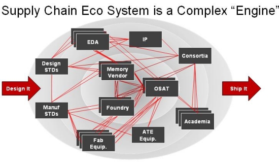
May 16, 2011 — Today at The ConFab, John Chen (Nvidia), Jeong-ki Min (Samsung Electronics), and Abraham Yee (Nvidia) gathered foundry, OSAT, and chip maker leaders to discuss what happens beyond Moore’s Law. The following are key points from "Collaboration to Strengthen the IC Supply Chain."

John Waite, VP, packaging development and central engineering at GLOBALFOUNDRIES, presented "Supply Chain Reaction: A Collaborative Approach to Packaging Innovation." Since packaging costs are the dominant contributor to the value chain, designers need to select the right combination of silicon and packaging technologies to achieve performance and cost goals.

What enables success in the More Moore realm? Waite lists diverse options for wafer bumping (lead-free, copper pillar, lead and high-lead solders used in bond on pad, repassivation or redistribution [RDL] designs) and package form factor (QFP/QFN, BGA and flip chip, wafer-level chipscale packages [WLCSP]), as well as vertical options that take advantage of Z space (stacked chips, system in package [SiP]). These each have tradeoffs of cost, time, and density/performance, and customers must make packaging choices with these goals in mind.

Click to Enlarge
Packaging influences the front end. SOURCE: John Waite, GLOBALFOUNDRIES.

Packaging increasingly requires attention on the frontend because of the packaging demand on the wafer. The frontend, backend, and system suppliers must collaborate in chip development. Early engagement, EDA tool flow optimization, turnkey wafer-to-package assembly, and other risk reduction strategies take a design from R&D into high-volume manufacturing.

Nick Yu, VP of technology development, Qualcomm, brought a fabless perspective to the session. In "3D Through Si Stacking Technology — a Qualcomm Perspective," Yu reminds us that 3D packaging creates thin, small, exciting products with long battery life. All 3D packages create better form factors on the board, increased performance for the device, and higher modularity in the design. The options to create a 3D package, however, as Waite also noted, are myriad: wire bonded chip stacks, flipped stacked chips, bumped/bonded chip stacks, through silicon vias (TSV) implemented as interposers, via first, or mid-process. Yu assesses these 3D technologies on the commercialization roadmap. Leading-edge technologies, like wide I/O memory on logic, are moving from lab to fab for the best of all worlds.

Click to Enlarge
Supply chain needs a 3D ecosystem, as 3D is disruptive to how we do things today. SOURCE: Nick Yu, Qualcomm.

While integrated fabless companies are ramping up leading-edge 3D IC designs, the lack of standards is holding back the 3D ecosystem. Traditional business models also don’t support the boundary-breaking 3D design and process steps. Yu supports integration via standards bodies and research consortia to bring design and manufacturing standards to the 3D arena. Consider Yu’s questions: Who owns the die? Who holds the inventory? How are pass-through costs funded? Who owns the integration process? Who owns the yield? Is the additional risk of TSV worth the benefits over wire-bonded stacks? Is a fabless design company or an IDM the way to go? The key question here is who acts as the "3D aggregator"? Foundry, memory company, OEM, fabless, OSAT?

Raj Pendse, VP of product and technology marketing at STATS ChipPAC and Robert Darveaux, CTO of Amkor, covered this supply chain integration from the dedicated packaging house perspective. Pendse presented "3D Packaging Evolution from an OSAT Perspective." Darveaux spoke on "Supply Chain Challenges for 3D Integration of Memory and Logic Devices using TSVs."

Click to Enlarge
Material flow and infrastructure evolution. SOURCE: Dr. Raj Pendse, STATSChipPAC Inc.

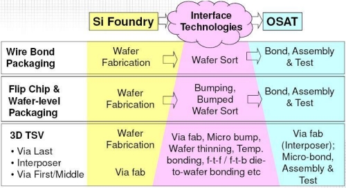
Pendse sees synergies and intersections among parallel developments in the three areas of packaging technology (i.e. traditional die and package stacking on substrates, fan-in and fan-out wafer level packaging and 3D Si integration). With these new process technologies, the OSAT industry’s role is transformed. Pendse channels wafer bumping, thinning, and other tasks into an in-between space for the Si foundry and OSAT to determine logical hand off points. Many of these processes can be done in both — the question to ask is who can do it better in each scenario? Is TSV fabrication best handled in the fab, with the OSAT taking over via fill and silicon interconnect? Pendse also spoke on "bridge" technologies — interposers, super-thin package-on-package, TSV hybridized with fan-out wafer-level packages (FOWLP) — that play an interim role in the commercialization of 3D. Pendse shared a typical OSAT TSV roadmap through 2013 with the attendees.

Darveaux compared the relative ease of sourcing, assembly, and test of package-on-package (POP) with the challenges of TSV: difficult to test high-density area array contact pads or bumps; bare or partially assembled memory and logic die that are difficult to burn in adequately; a newer joining technology not widely available to OEMs and contract assemblers; a poorly characterized joining process yield; and, due to the immaturity of the test, burn-in, and assembly; unclear ownership of defect liability. This applies to the "2.5D" interposer strategy as well as pure 3D TSV stacks. Interconnect processes are too new and done in too small sample sizes to lead to industry agreement on the right method: die-to-die first or die-to-laminate first? Interposer in singulated format or wafer format?

Click to Enlarge Click to Enlarge
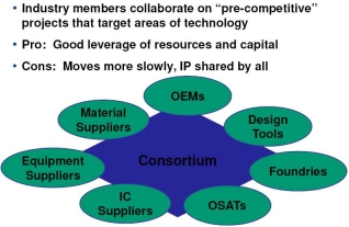
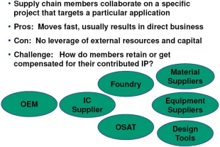
Consortium collaboration model. Supply chain collaboration model. SOURCE: Robert Darveaux, Amkor Technology.

These problems can not be resolved by technologies or business models alone. TSV processes can be standardized and characterized, with the resource-sharing model of consortia or the faster but potentially messy supply chain collaboration on specific projects. Both offer pros and cons, and fit different needs of the industry.

More from The ConFab:

May 13, 2011 — Yole Développement released "Equipment & Materials for 3DIC and Wafer-Level-Packaging," a database and complete report analyzing in detail the equipment and materials tool-box for wafer-level packaging (WLP).

Wafer-level packaging is the name given to an array of technologies: historically flip-chip wafer bumping with electroplated gold and solder bumps and leading-edge copper pillars. Form factors include fan-in WLCSP packages, 3D WLP, FO WLP packages, 2.5D glass/silicon interposers and 3DIC integration with TSV interconnects.

A real infrastructure has emerged into what is now being called the mid-end of the semiconductor manufacturing environment (the overlapping area that is served by IDM/CMOS foundry backend of line [BEOL] processes and the OSAT/wafer bumping house back-end wafer bumping assembly). There’s a significant difference in how manufacturing is generally performed in the front-end versus the back-end.

Yole’s analysts gathered all the information necessary to benchmark and compare all the different alternatives offered by the present equipment and material tool-box for wafer-level-packaging. All main scenarios are analyzed, including flip-chip wafer bumping trends, Fan-in WLCSP, 3D WLP, FOWLP, 2.5D silicon interposers, 3DIC Via Middle & Via Last processes. Yole includes a 2010-2016 wafer forecast for each "flavor."

The backend has greater cost sensitivity with adaptability for scaling with time, as ICs shrink and pin counts increase. Frontend technologies are more expensive initially, but offer higher repeatability, yield, and throughput. Frontend technologies allow chip makers to scale down the technology to smaller pitch dimension while maintaining cost pressure.

Future trends for PANEL scale packaging (embedded die in PCB, FOWLP 2nd generation and polysilicon or glass sheet interposers based on LCD/PCB/Solar infrastructures) are also analyzed.

WLP has emerged as the fastest growing semiconductor packaging technology with more than 27% CAGR in unit shipments over the next 5 years. The wafer-level-packaging market shows the greatest potential for significant  future growth in the semiconductor industry. Yole expects the equipment and material market for wafer-level packaging to grow significantly in total revenue over the next five years with a CAGR over 60%. The growth will be mainly driven by the expansion of flip-chip, WLCSP and FOWLP technologies into the wireless mobile industry along with the emergence of 3DIC technology into 3D TSV stacked memories, wide I/O interfaces in logic and memory ICs as well as in CMOS image sensors, MEMS and other heterogeneous 3D stacking applications.

The analysis quantifies the WLP equipment market evolution for wafer bonders, die pick & place bonders, C2W bonders, DRIE etching & drilling tools, CVD, PVD, plating, exposure & lithography, spray coating, temporary bonding & de-bonding, grinding-thinning-CMP, wafer-molding, inspection & metrology, and test tools.

On the material side, it covers photoresist & coatings, adhesive tapes, pre-applied & wafer-level underfills, molding compounds, thermal interface materials (TIM), plating/etching/cleaning chemistries, slurries for CMP, temporary bonding materials, gas & precursors, sputtering targets, silicon & glass wafer carriers, cap, 2.5D interposer and TSV substrates.

Wafer-level packaging tool providers are consolidating, Yole says, pointing to Applied Materials’ acquisition of Semitool, which enabled AMAT to expand and sustain in this back-end/WLP direction.

Along with this new research report, Yole will be delivering a 350+ players excel database screening and profiling the detailed activity of small, medium, and giant equipment & material suppliers coming either from Front-end, Back-end assembly, PCB, LCD or Solar industries and providing actual solutions for the 3DIC & wafer-level-packaging tool-box.

WLP equipment & material market forecasts are given in unit, volume and revenues 2010-2016, with estimated sales opportunities in the global mid-end 3DIC & wafer-level-packaging area.

Report authors:
Phil Garrou recently joined Yole Développement forces as senior technical advisor in the fields of advanced packaging. He blogs for ElectroIQ.com at Insights from the Leading Edge.

Jerome Baron is leading the advanced packaging market research at Yole Developpement.

Access the report at http://www.i-micronews.com/reports/Equipment-Materials-3DIC-Wafer-Level-Packaging/204/

Subscribe to Solid State Technology/Advanced Packaging.

Follow Advanced Packaging on Twitter.com by clicking www.twitter.com/advpackaging. Or join our Facebook group

May 13, 2011The ConFab gathers semiconductor industry leaders to discuss the biggest trends in the chip manufacturing sector. One of these major trends is 3D packaging. In Session 2 on Monday (May 16), John Waite (GLOBALFOUNDRIES), Raj Pendse (STATS ChipPAC), Robert Darveaux (Amkor), and Nick Yu (Qualcomm) will combine fabless, foundry, and packaging house perspectives on the disruptive design and process changes that 3D creates for the semiconductor and packaging industries.

John Chen (Nvidia), Jeong-ki Min (Samsung Electronics), and Abraham Yee (Nvidia) will lead "Collaboration to Strengthen the IC Supply Chain."

Smaller dimensions and higher complexity chips are driving "More Moore," while "More than Moore" is pushing vertical integration, such as 3D TSV. Both require changes to the traditional frontend and backend of semiconductor manufacturing.

3D packaging, whether bonded wafers with through silicon vias (TSV) or wire bonded chip stacks, push packaging processes into the fab, and make wafer-level processes the outsourced semiconductor assembly and test (OSAT) provider’s responsibility. In this new supply chain, many questions are raised about ownership and responsibility in the implementation of a new chip design. Since our IC industry has long been divided into EDA or fab tool supplier, fabless, foundry and assembly/test companies, getting everyone to work together and make profits for each party can be extremely challenging. This session is intended to explore various options.

Session 2, "Collaboration to Strengthen the IC Supply Chain" presentations:

John Waite, VP, packaging development & central engineering, GLOBALFOUNDRIES: Waite will present "Supply Chain Reaction: A Collaborative Approach to Packaging Innovation." As the industry moves aggressively to more advanced technology nodes, the once "bland" interconnect, assembly and packaging processes can now improve performance and power efficiency as well as reduce costs for chip designers. Chip-package interaction (CPI) is significantly more complex today, requiring coordination between design and manufacturing. It is increasingly difficult for foundries and OSATs to be able to deliver end-to-end solutions that meet the requirements of leading-edge designs. A new approach is needed — one that leverages the success of a "shared investment, shared return" model.

Raj Pendse, VP product & technology marketing, STATS ChipPAC: Pendse will present "3D Packaging Evolution from an OSAT Perspective," illustrating the synergies and intersections among packaging technologies (i.e. traditional die and package stacking on substrates, fan-in and fan-out wafer level packaging and 3D Si integration) and the resulting future path for packaging technology. Pendse will discuss the transformed role of the OSAT industry in supporting this evolution. Latest developments in wafer thinning, micro bumping, micro bonding and logical hand off points among Si and package foundries will be presented, and Pendse will look at "bridge" technologies — interposers, TSV substrates — that play an interim role in the commercialization of 3D.

Robert Darveaux, CTO, Amkor: Darveaux will present "Supply Chain Challenges for 3D Integration of Memory and Logic Devices using TSVs." While package-on-package (POP) technology allows ease of test, flexible sourcing, and mature interconnect technology, TSV technology suffers from difficult-to-test high-density area array contact pads or bumps; bare or partially assembled memory and logic die that are difficult to burn in adequately; a newer joining technology not widely available to OEMs and contract assemblers; a poorly characterized joining process yield; and ultimately unclear ownership of defect liability. These problems can not be resolved by technologies or business models alone.

Nick Yu, VP of technology development, Qualcomm: Yu is presenting "3D Through Si Stacking Technology – a Qualcomm Perspective." Qualcomm, as an integrated fabless company, has several primary motivations for following 3D TSV-based stacking technologies. Yu will propose a roadmap for the evolution of the 3D technology, and detail the integration challenges for an integrated fabless manufacturer using a distributed supply chain. Yu shares Qualcomm’s implementation strategy, and points to some of the gaps in the business model associated with 3D products.

See The ConFab’s conference program here.

Bios:

Session Leaders:
John Chen, Ph.D., VP of technology and foundry operations, Nvidia: Dr. Chen has 30 years of experience in IC industry ranging from IDM to Foundry to Fabless companies. Dr. Chen was a Howard Hughes Doctor Fellow and received a Ph.D. in EE and an Executive Management degree, both from UCLA. He also holds a M.S. from University of Maine and a B.S. from National Taiwan University, both in E.E. He started his career as a researcher in Hughes Research Laboratories, subsequently at Xerox Palo Alto Research Center (PARC). Most of his work involves CMOS devices and process technologies. Later, he has had various technical and managerial positions in technology development and IC manufacturing. He has held positions at Cypress Semiconductor, TSMC, WaferTech (a JV then led by TSMC), and Nvidia. Dr. Chen has published 100 papers, mostly by IEEE and a book, "CMOS Devices and Technology for VLSI." Accolades and industry service include IEEE Fellow, Technical Advisory Committee for ITRI, Taiwan, and committee member of SIA and GSA.

Jeong-ki Min, VP of foundry marketing, Samsung Electronics Co., Ltd. LSI Division: Jeong-ki Min joined Samsung in 1984 and has served in marketing, technology planning, and capital investment to M&A and other strategic alliances. He also worked for Samsung’s US operations (San Jose, CA), as a planning officer. Min leads foundry and ASIC marketing teams and his current responsibility at System LSI Division includes business development and market research and customer engineering supports.

Abraham Yee, director of advanced technology & package development, Nvidia Corporation: Yee is responsible for readying next generation technologies for production, benchmarking technologies, investigating new technologies and setting NVIDIA’s process roadmap. Prior to NVIDIA, he has worked with SUN Microsystems, Equator Technologies, and LSI Logic Corp. Dr. Yee received his BA in Mathematics and Physics and his PhD in Physics from UC Berkeley.

Speakers:
Waite is responsible for global packaging development and collaborative R&D activities, as well as central engineering. Waite joined GLOBALFOUNDRIES in 2009 after a 25-year career in technical and management positions at AMD and IBM.

Pendse completed his BS in Materials Science from IIT Bombay with Top in Class honors and his Doctorate in Materials Science from UC Berkeley. Prior to joining STATS ChipPAC, Raj held various positions in package engineering and R&D at National Semiconductor Corp and Hewlett-Packard Labs. His work has spanned the gamut from packaging of high-end microprocessors, ASIC and graphics products to low-cost packaging solutions for logic and analog devices used in mobile phones and consumer products. His most recent focus has been on flip chip and 3D wafer level packaging.

Darveaux has 24 years experience in the IC packaging field at the Microelectronics Center of North Carolina, Motorola, and Amkor. Robert has a B.S. in Nuclear Engineering from Iowa State University and a Ph.D. in Materials Science and Engineering from North Carolina State University. His expertise covers thermal and mechanical simulation, materials characterization, failure analysis, and fatigue life prediction for solder joints. Robert has published over 75 technical papers and has 22 patents.

Yu is a Vice President of Engineering at Qualcomm’s CDMA Technologies Division. He sets Qualcomm’s semiconductor technology roadmaps including wafer fab process node, backend interconnect and packaging technologies. Yu has 18 years of experience with Qualcomm on low power wireless chipset and SoC development. He is one of the architects of, and has participated in the definition and development of, many Qualcomm chipset products. Nick has an MSEE degree from Georgia Institute of Technology.

May 12, 2011 — Rudolph Technologies, Inc. (NASDAQ: RTEC), process characterization equipment and software provider to wafer fabs and advanced packaging facilities, released the Wafer Scanner 3880 inspection and measurement system for advanced packaging applications.

The first production system was delivered in March 2011 to a major semiconductor foundry, which cited throughput and flexibility as benefits of the system. A second system shipped to a leading IDM, where it will be used to develop new packaging processes.

The WS 3880 provides 3D (height) and 2D measurement and inspection of micro and standard bumps, through silicon via (TSV) post-via-fill copper protrusions (nails) and re-distribution layers (RDL) used in 3D IC packaging. It also offers an ultra-high resolution 3D sensor designed for micro bumps as small as a few microns. The WS 3880 inspects flip chip and non-flip-chip wafers. According to Reza Asgari, Rudolph Wafer Scanner product manager, "Micro bumps, TSVs and RDLs are critical interconnect technologies used in 3D IC packages; the new WS 3880 provides the 2D and 3D measurement and inspection capability required to develop and maximize yields for these packaging processes. Ultra-high resolution allows the Wafer Scanner to accurately characterize small features, such as micro bumps and TSV nails…while still preserving the flexibility to handle standard bumps and other larger features."

Rudolph’s proprietary 3D laser triangulation technology measures bump height and coplanarity, RDL thickness, and more.

The WS 3880 suits high-volume manufacturing, for either randomly sampled inspection or 100% inspection. The system permits on-line or off-line defect review and classification. Electronic wafer maps can be imported into the system, updated after inspection and exported.

The WS 3880 replaces the 3840 system, launched immediately following Rudolph’s acquisition of RVSI assets in 2008. Over 20 WS 3840 systems have been installed in advanced packaging facilities.

Rudolph Technologies, Inc. is a worldwide leader in the design, development, manufacture and support of defect inspection, process control metrology, and data analysis systems and software used by semiconductor device manufacturers. Additional information can be found at www.rudolphtech.com

Subscribe to Solid State Technology/Advanced Packaging.

Follow Advanced Packaging on Twitter.com by clicking www.twitter.com/advpackaging. Or join our Facebook group

May 12, 2011 – BUSINESS WIRE — Tessera Technologies, Inc. (NASDAQ: TSRA) Board of Directors appointed Robert A. Young, Ph.D., as president and chief executive officer (CEO). Young is currently a member Tessera’s Board of Directors. Young will take over for Henry R. Nothhaft, who resigned to pursue his advocacy of smart innovation policies in Washington, as presented in his recently released book Great Again – Revitalizing America’s Entrepreneurial Leadership (Harvard Business Press).

Nothhaft will continue to serve as chairman of the board of directors until May 20, 2011, shortly before the company’s upcoming 2011 annual meeting of stockholders, and will remain in a non-executive advisory role to assist Tessera with various endeavors thereafter. Robert J. Boehlke will succeed Nothhaft as chairman. Boehlke is currently a member of Tessera’s Board of Directors.

Tessera recently announced plans to refocus the company beyond the semiconductor packaging arena, including a possible separation of its Imaging & Optics business. "Under Hank’s leadership, the company made numerous operational improvements and experienced growth, both organic and acquired," noted Young.

"This is a very exciting time in the company’s history, given the opportunities we see to maximize long-term shareholder value," continued Young. "The investments made in the last several years have positioned us well to take advantage of two rapidly growing and changing markets: consumer optics and intellectual property. The board has initiated efforts to re-structure the businesses to take full advantage of these emerging opportunities."

"Tessera is a great company, with an exciting future ahead, and I am reluctant to leave," said Henry R. Nothhaft. "But the impact on our economy of national innovation policies, including the patent reform legislation currently pending in Congress, presents a significant challenge at this critical juncture. This is where I’d like to focus my time and efforts now."

Young has served as a member of Tessera’s board of directors since its inception in 1991. He has had a broad career including 17 years at IBM Corporation, where he held various executive positions. Subsequently, Young served as the managing partner of Dillon, Read & Co., Inc.’s venture capital operation before serving as Dillon, Read & Co.’s head of Technology Banking. He has a Ph.D. in physical chemistry from the Massachusetts Institute of Technology and a B.S. with honors in chemistry from the University of Delaware.

Management held a conference call available for replay for 90 days at www.tessera.com. In addition, a replay of the call will be available via telephone for two business days. To listen to the telephone replay in the U.S., please dial 800-642-1687 and for international callers, dial 706-645-9291. Enter access code 66825888.

Tessera Technologies, Inc., headquartered in San Jose, California, develops, invests in, licenses and delivers innovative miniaturization technologies and products for next-generation electronic devices. For information, go to www.tessera.com.

Subscribe to Solid State Technology/Advanced Packaging.

Follow Advanced Packaging on Twitter.com by clicking www.twitter.com/advpackaging. Or join our Facebook group

May 11, 2011 – BUSINESS WIRE — CoolChip Technologies won the MIT Clean Energy Prize for their technology that reduces data center cooling needs.

CoolChip helps data centers reduce cooling costs using patented technology to eliminate the thermal barrier that currently stifles the performance of a computer’s central processing unit (CPU). Comprised of a team of engineers and business professionals with extensive experience in information technology and thermo-mechanical engineering, CoolChip is dedicated to delivering the next generation of ultra-high efficiency air-based CPU coolers.

Other work on data center thermal management include hot-water cooling (IBM Zurich) and source-located thermal management (Nextreme Thermal Solutions).

CoolChip was selected from 80 teams from over 40 universities by prominent judges.

The MIT Clean Energy Prize is a national competition founded in 2008 by MIT, the U.S. Department of Energy and NSTAR to accelerate the pace of clean energy entrepreneurship and boost the clean energy economy.

Now in its fourth year, the MIT Clean Energy Prize is helping to jump-start the clean energy industry while creating jobs. In just three years it has helped form over two dozen companies that have already raised over $80 million in investment capital and research grants.

For additional information on the MIT Clean Energy Prize, please visit www.mitcep.org.

NSTAR is the largest Massachusetts-based, investor-owned electric and gas utility. For more information, visit www.nstar.com.

To learn more about Massachusetts Institute of Technology (MIT), visit www.mit.edu.

Subscribe to Solid State Technology/Advanced Packaging.

Follow Advanced Packaging on Twitter.com by clicking www.twitter.com/advpackaging. Or join our Facebook group