Category Archives: Wafer Level Packaging

April 6, 2011 — Keithley Instruments Inc., advanced electrical test instruments and systems provider, introduced the Model 2651A High Power System SourceMeter instrument to characterize high-power electronics.
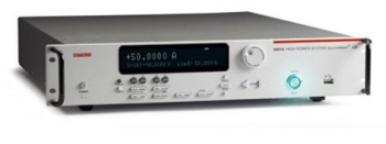
Click to EnlargeThe Model 2651A claims the widest current range available in the industry, suiting R&D, reliability, and production test applications, such as testing high-brightness LEDs (HB-LEDs), power semiconductors, DC-DC converters, batteries, and other high-power materials, components, modules, and subassemblies.

Like each member of the Series 2600A family, the Model 2651A offers a highly flexible, four-quadrant voltage and current source/load coupled with precision voltage and current meters. It combines the functionality of multiple instruments in a single full-rack enclosure: semiconductor characterization instrument, precision power supply, true current source, DMM, arbitrary waveform generator, V or I pulse generator, electronic load, and trigger controller, and is fully expandable into a multi-channel, tightly synchronized system via Keithley’s TSP-Link technology. The Model 2651A can source or sink up to 2,000W of pulsed power (±40V, ±50A) or 200W of DC power (±10V@±20A, ±20V@±10A, ±40V@±5A). It can also make precise measurements of signals as low as 1pA and 100 microvolts at speeds up to one microsecond per reading.

The user can chose digitizing or integrating measurement modes for precise characterization of both transient and steady-state behavior. Two independent analog-to-digital (A/D) converters define each mode — one for current and the other for voltage — which run simultaneously for accurate source readback.

The digitizing measurement mode’s 18-bit A/D converters allow capturing up to one million readings per second for continuous one-microsecond-per-point sampling, making this mode the most appropriate choice for waveform capture and measuring transient characteristics with high precision. Competing solutions must average multiple readings to produce a measurement result and often don’t allow the measurement of transient behavior.

The integrating measurement mode, based on 22-bit A/D converters, optimizes the instrument’s operation for applications that demand the highest possible measurement accuracy and resolution. This ensures precise measurements of the very low currents and voltages common in next-generation devices. All Series 2600A instruments provide integrating measurement mode operation.

Connecting two Model 2651A units in parallel via TSP-Link expands the system’s current range from 50A to 100A. This is 2.5-5x greater than the nearest competing solution. The voltage range can be expanded from 40 to 80V when two units are connected in series. The embedded Test Script Processor (TSP) included in all Series 2600A instruments simplifies testing by allowing users to address multiple units as a single instrument so that they act in concert. The built-in trigger controller in the Model 2651A can synchronize the operation of all linked channels to within 500 nanoseconds. These capabilities of the Model 2651A provide the broadest dynamic range available in the industry, making the unit suitable for a broad variety of high current, high power test applications, including:

  • Power semiconductor, HBLED, and optical device characterization and testing
  • Characterization of GaN, SiC, and other compound materials and devices
  • Semiconductor junction temperature characterization
  • Reliability testing
  • High speed, high precision digitization
  • Electromigration studies

To minimize device self-heating during tests, a common problem with high-power semiconductors and materials, the Model 2651A offers high-speed pulsing capabilities that allow users to source and measure pulses with high accuracy. Pulse widths from 100 microseconds to DC and duty cycles from 1 to 100% are programmable. Competing solutions are typically hampered by limited flexibility for programming the instrumentation’s duty cycle.

TSP Express, Keithley’s LXI-based I-V test software utility, is embedded in the instrument. From basic to advanced tests, TSP Express delivers device data in three easy steps: connect, configure, and collect. It also simplifies connecting instruments to allow higher pulsing levels. Results can be viewed in either graphical or tabular format and then exported to a .csv file for use with spreadsheet applications. Two other powerful software tools for creating test sequences are also provided. The Test Script Builder application supports creating, modifying, debugging, running, and managing TSP scripts. An IVI-based LabVIEW driver simplifies integrating the Model 2651A into LabVIEW test sequences.

To learn more, visit the Model 2651A product page: http://www.keithley.com/products/dcac/currentvoltage/highcurrent/?mn=2651A

Subscribe to Solid State Technology/Advanced Packaging.

Follow Advanced Packaging on Twitter.com by clicking www.twitter.com/advpackaging. Or join our Facebook group

April 6, 20111 – MarketwireVerigy (NASDAQ: VRGY), semiconductor test provider, won new business with Freescale Semiconductor’s Networking and Multimedia Group (NMG), which has placed a volume order for Verigy’s V93000 scalable test platform to use in testing select QorIQ PowerPC communications microprocessors, based on Power Architecture technology.

Freescale’s NMG conducted an extensive evaluation of the V93000 platform in which comparative performance testing was done using a multi-core, high-speed networking device. NMG found that the V93000’s tester-per-pin architecture was cost effective and reduced testing cycle times.

The scalability and flexibility of the V93000 platform enables NMG to use Verigy’s testers on some QorIQ processors as well as select products incorporating DDR III and PCIE II, adding versatility to the chipmaker’s in-house testing resources.

"Our evaluation found that the V93000 delivered an advanced technical solution with a low cost of test," said Bill McKean, chief procurement officer for Freescale. "Verigy’s knowledge and experience were also critical to our decision."

The V93000 platform has the flexibility to test a wide range of semiconductor devices used in a variety of end products, from digital televisions to wireless communication devices. The tester claims accuracy and high throughput. The V93000 platform has been used in developing and producing multiple generations of logic and high-speed memory ICs at integrated device manufacturers (IDMs), fabless companies, outsource assembly and testing (OSAT) houses, and foundries.

Verigy provides advanced semiconductor test systems for design validation, characterization, and high-volume manufacturing test. Additional information about Verigy can be found at www.verigy.com.

Subscribe to Solid State Technology/Advanced Packaging.

Follow Advanced Packaging on Twitter.com by clicking www.twitter.com/advpackaging. Or join our Facebook group

April 5, 2011 – PRNewswire — MagnaChip Semiconductor Corporation (NYSE: MX), a Korea-based designer and manufacturer of analog and mixed-signal semiconductor products, now offers cost-competitive and state-of-the-art copper wire bonding technology for semiconductor foundry customers. 

Copper bonding uses copper wires instead of gold for interconnection and has become one of the most preferred methods to reduce overall package cost for semiconductor applications, as the price of gold continues to rise.

Copper is three to five times less costly than gold. Substituting gold with copper can achieve a packaging cost savings of about 20% to 30%.  Copper wire is about 30% more conductive than gold, making it a superior electrical conductor. Copper also has about 25% higher thermal conductivity. Because of copper’s lower tendency to form intermetallic compounds, copper bonds can offer higher reliability at elevated temperatures than gold bonds.

One of the major challenges of copper wire bonding has been the significant mechanical stress imposed on bonding pads, which often resulted in damage to silicon wafers, causing cracks beneath the pads. To resolve this issue, MagnaChip worked with the major packaging companies, including Amkor, to develop and qualify an enhanced silicon bonding process.

MagnaChip Semiconductor is a Korea-based designer and manufacturer of analog and mixed-signal semiconductor products for high-volume consumer applications.

Subscribe to Solid State Technology/Advanced Packaging.

Follow Advanced Packaging on Twitter.com by clicking www.twitter.com/advpackaging. Or join our Facebook group

April 4, 2011 – BUSINESS WIRE — SiliconBlue Technologies unveiled its mobileFPGA platform device roadmap using TSMC’s 40nm low-power standard CMOS process. MobileFPGA platform families offer reduced power and 30-50% increased performance in comprehensive product families comprised of over 15 new devices, all with footprints smaller than 50 mm2.

"Los Angeles" incorporates advanced interface support for emerging standards such as SLIMbus and USB 2.0-based HSIC and ULPI, targeting sensor management and port expansion requirements that are being driven by the explosion of sensors and other peripherals in handheld applications.

"San Francisco" incorporates 1080p support with HDMI and MIPI interfaces. It has been designed for video, multi-display, and high-bandwidth memory interface applications, targeting the convergence of video and image content being simultaneously viewed on home and handheld devices.

The two distinct families target the two areas where smartphones and other handhelds differentiate, said Kapil Shankar, CEO of SiliconBlue. "These devices will be available for designs this year, in time to support the explosion in new handheld products."

More details regarding SiliconBlue’s 40nm-based mobileFPGA devices will be announced in 2Q2011.

SiliconBlue Technologies Custom Mobile Device solutions target handset applications, including IP, design services and a new class of ultra-low power, single-chip, CMOS SRAM mobileFPGA devices with patented non-volatile configuration memory (NVCM). Visit http://www.siliconbluetech.com.

Subscribe to Solid State Technology/Advanced Packaging.

Follow Advanced Packaging on Twitter.com by clicking www.twitter.com/advpackaging. Or join our Facebook group

April 4, 2011 – BUSINESS WIRE — Thin Film Electronics ASA (Thinfilm) and PARC, a Xerox company, entered the next phase of their co-innovation engagement for printed memory devices. This next phase extends the engagement to prototyping the product for manufacturing readiness.

PARC and Thinfilm’s collaboration on next-generation printed memory solutions kicked off last year with joint design of Thinfilm 128-bit Addressable Memory, which combines Thinfilm’s non-volatile memory (NVM) technology with PARC’s printed CMOS transistor technology.

Thinfilm will use the PARC CMOS technology to expand the memory technology that it has previously commercialized in a roll-to-roll (R2R) printed production process to an addressable version that is still fully printed. Products with Thinfilm addressable memory will be a key avenue for PARC to commercialize its technology.

"Our mutual goal is to reach the printed addressable memory prototype by the end of this year. Key work is already being done at PARC, working closely with Thinfilm’s engineers," said Dr. Ross Bringans, VP of PARC’s Electronic Materials and Devices research. "Thinfilm will utilize PARC background IP for the printed memory application."

"We expect to transfer the contact-based 128-bit memory array to production in 2012. This addressable memory meets the need for creating ubiquitous low-cost tags and disposable printed systems," Davor Sutija, Thinfilm CEO said.

Such memory enables unique form factors, cost advantages, and integration with other printed components including sensors and simple displays that can be customized for multiple markets — ranging from games and toys, to ID tags, disposable sensors, and price labels, notes Ana Arias, co-head of Thinfilm’s Technology Council, U.C. Berkeley Associate Professor in EECS.

To learn more about Thinfilm, please see www.thinfilm.no.

To learn more about PARC, please see: www.parc.com.

Subscribe to Solid State Technology/Advanced Packaging.

Follow Advanced Packaging on Twitter.com by clicking www.twitter.com/advpackaging. Or join our Facebook group

By Debra Vogler, senior technical editor

April 1, 2011 — Daniel Duffy, research scientist in Henkel’s Advanced Technology Group, was a presenter at MEPTEC’s The Heat is On event (3/21/11, Santa Clara, CA). Summarizing the encapsulant materials used for high-brightness LEDs (HB-LEDs), he noted the pros and cons of epoxy and silicone. The material challenges for epoxies are temperature stability and color (aging); and for silicone, contamination and adhesion, as well as barrier properties. In the future, epoxies will have to be stable with respect to blue light (T>150ºC); and silicone material will have to fulfill the condition T<Tg CTE <60ppm/K. "Silicone encapsulants are very stable," said Duffy. "But it is not enough — future power demands require higher levels of photo-thermal stability."

Die attach material challenges include transparency, CTE, interfacial TC, and adhesion properties. Such materials will need to have stable thermal resistance, high TC, matched TCE, and good adhesion properties. Duffy specifically mentioned adhesion as a critical property for LED packaging. "Delamination leads to increased interfacial thermal resistance," said Duffy. "Localized temperature increases can shorten device life." Furthermore, cracking can lead to weakening of wire bonds and cracks; also, delamination weakens barrier protection.

In this podcast interview, Duffy discusses the outlook for new materials and/or enhanced materials for HB-LED applications, including quantum dots. "Quantum dots are very interesting materials…when we learn how to tune the interactions between then and the rest of the materials involved in LED packaging, they will play a continuous role in the future," said Duffy. "They offer a wide variety of colors, tunability of color, and lots of options for tuning their performance with temperature, with time and, maybe even other optical effects we’re not even considering now…they’re here to stay."  The challenge, he noted, will be getting them into materials for higher-power applications.

Listen to Duffy’s podcast interview:  Download (iPhone/iPod users) or Play Now


Subscribe to Solid State Technology/Advanced Packaging.

Follow Advanced Packaging on Twitter.com by clicking www.twitter.com/advpackaging. Or join our Facebook group

Click to EnlargePhil Garrou,
Contributing Editor

The status of semiconductor packaging roadmaps was the focus of a forum hosted late last year by MEPTEC (Microelectronics Packaging and Test Engineering Council), a trade association of semiconductor suppliers and manufacturers. MEPTEC brought together a group of experts from AMD, Altera, Amkor, ASE, Cisco, LSI, Micron, TechSearch, Unisem, Yole and other companies and organizations.

Bill Bottoms, CEO of 3MTS gave the introductory talk taking a look a collaborative roadmaps and international roadmap perspectives. From his position as chair of the ITRS (International Technology Roadmap for Semiconductors) packaging and assembly TWG (technical working group) Bill reminded attendees that ITRS is sponsored by Europe, Japan, Korea, Taiwan and the US to forecast semiconductor technology requirements 15 years out, and to forecast emerging semiconductor devices and materials 10 years out.

In addition to the ITRS, i-NEMI is the pivot point for all microelectronic packaging activities of a variety of organizations, including IMAPS, IPC, INSIC, OIDA, IEEE, CPMT and USDC. On a global basis, the other organization looking at overall semiconductor packaging solutions is JISSO, a Japanese term which reflects the total packaging solution for electronic products.

Bottoms’ premise is that for the past 40 years semiconductor progress could be easily predicted. The focus was on design and fab. Semiconductor roadmap goals were all clearly focused on shrinking geometries (scaling) and increasing wafer size. However, as we enter the "deep submicron" era, things become more complicated and packaging becomes more important in delivering semiconductor yield, reliability and performance.

The answer developed to address the historical lack of package scaling to match IC scaling was to generate the packaging at the wafer level, i.e. wafer level packaging or WLP. WLP, now firmly entrenched as a packaging option, offers portable consumer products several benefits: inherently lower cost, better electrical performance, lower power requirements, and smaller size.

Another important trend in packaging is the incorporation of multiple die into a single package or what has become known as System in Package (SiP), or MCM (to those of us that have been around awhile).

Moving forward, Bottoms predicts, as many of us do, that the 3rd dimension will be the key enabler in maintaining the "price elastic growth of the electronics industry." While 3D presents many challenges they all appear to have reasonable solutions. 3D will appear first through silicon interposers with through wafer connections and then through chips fabricated with internal TSV for through wafer connections.

Bill updated attendees with where the packaging roadmap would be increasing and expanding coverage in 2011. Bottoms concludes that the pace of change in packaging technology has never been greater and roadmaps are critical to continuation of this rate of progress.

Bryan Black of AMD looked at why 3D is required if semiconductor technology is to continue to move ahead. In standard fashion Black defines 3D technology in two varieties: TSV in active devices and TSV on interposers.

From a systems standpoint Black proposes the interesting perspective that performance density drives new form factors, new form factors discover new usage models and without new form factors the industry would stagnate.

The latest edition of the ITRS notes that the expansion of 3D architectures for packaging poses unique challenges that are not encountered in conventional 2D packaging. These include: Thinning wafers and die, and the handling of these thinned wafer and die; Thermal management when several layers of semiconductor devices are stacked; Power delivery and the maintenance of power integrity as the operating voltages are dropped to near the threshold voltage; and testing for 3D structures when test access is a challenge.

More Solid State Technology Current Issue Articles
More Solid State Technology Archives Issue Articles

March 31, 2011 — Sigurd Microelectronics Corporation (Sigurd) will be the first adopter of Multitest’s MT2168 pick-and-place test handler in volume production in Taiwan. The SATS provider will use it to test various QFN packages.

Sigurd, an independent provider of semiconductor assembly and test services (SATS), is known for being a pioneer in employing new IC assembly and test equipment and technologies. Responding to the market requirements, Sigurd continuously improves and upgrades its technology and equipment base.

The recently installed MT2168 ambient-hot pick-and-place handler is used for a hot test application of various small QFN packages. Using the handler in a high-volume environment, Sigurd decided on the fully automated, 16 contact site version of the scalable platform.

After running production tests for several weeks, Sigurd experienced significant advantages from the optimized test cell utilization. Excellent handler jam rate and high soak buffer design allowed the company to almost double daily output.

Sigurd Microelectronics Corporation’s test services cover a wide range of both standard and customized test solutions, including C/P and F/T for logic, analog, mixed-signal, RF, memory and power. The products assembled and tested by the company are extensively used in wireless communication, computing, digital consumer and multimedia products. Sigurd’s customers include many of the world’s leading semiconductor design houses, IDMs and wafer foundries. For more information, visit www.sigurd.com.tw.

Multitest manufactures test equipment for semiconductors, including test handlers, contactors, and ATE printed circuit boards. For more information, visit www.multitest.com.

Subscribe to Solid State Technology/Advanced Packaging.

Follow Advanced Packaging on Twitter.com by clicking www.twitter.com/advpackaging. Or join our Facebook group

By Debra Vogler, senior technical editor

March 31, 2011 — Serial entrepreneur, Zvi Or-Bach, was interviewed by ElectroIQ about his latest startup, MonolithIC 3D. In this podcast interview, Or-Bach explains why the company changed its name (from NuPGA) when its mission changed. "The name change was in response to a strategic change we made once we discovered a path to monolithic 3D ICs," said Or-Bach. He noted that on-chip interconnects are the limiting aspect with respect to scaling, and that after making materials changes (i.e., Al to Cu, and SiO2 to low-k), the only solution is to go to 3D ICs.

Listen to Or-Bach’s interview:  Download (iPod/iPhone users) or Play Now

Interconnect delay → Monolithic 3D   Implant H+ dummy gates Transfer on top of processed wafer and replace gates (<400°C)
  90nm (2005) 45nm (2010) 22nm (2015) 12nm(2020)
Transistor delay 1.6ps 0.8ps 0.4ps 0.2ps
Delay of 1mm-long interconnect 5 x 10²ps 2 x 10³ps 1 x 10⁴ps 6 x 10⁴ps
Ratio 3 x 10² 3 x 10³ 4 x 104 3 x 10⁵
3D 

Figure. Next-generation monolithic 3D IC — leveraging the gate-last process. SOURCE: MonolithIC 3D

Semiconductor scaling costs

Scaling down 0.7x Scaling up (3D packaging)
 Cost: Capital >$4B  Cost: Capital: <$200M
   R&D >$1B   R&D  <$100M 
 Benefits: Die size 0.5x Benefits:  Die size 0.5x 
  Power 0.5x   Power 0.5x
Speed: No change Speed: No change

Table. The next-generation dilemma — going up or going down? Companies can do both. SOURCE: MonolithIC 3D. 

"While TSVs are a big help with off-chip interconnects, they are not helpful for on-chip interconnects — they are just too large," explained Or-Bach. "Our vertical interconnect is 10000× more dense than TSVs." The company’s mission is an answer to what Or-Bach calls the next-generation dilemma (table). Whether one chooses to continue to scale down 0.7×, or scale "up" by going to 3D, there are costs. However, the company’s estimates show a glaring difference: capital costs and R&D costs are, respectively, >$4B and >$1B for scaling down; and <$200M and <$100M for scaling up.

3D IC technology

The technology being proposed by Or-Bach uses a combination of four ideas:
1) the gate-last process and proper sequencing of ion-cut (i.e., Smart Cut) technology;
2) low-temperature face-up layer transfer;
3) repeating layouts;
4) innovative alignment.

Or-Bach explains the process in detail (figure) in his audio interview. The technology still requires process development work, but looking ahead, Or-Bach views it as being applicable to both Tier 2 fabs that want to reinvent themselves and compete with leading-edge fabs, and leading-edge fabs that want to add value.

Subscribe to Solid State Technology/Advanced Packaging.

Follow Advanced Packaging on Twitter.com by clicking www.twitter.com/advpackaging. Or join our Facebook group

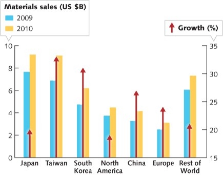
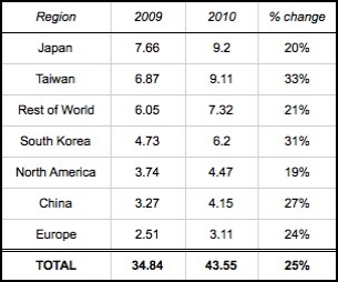
March 29, 2011 – Sales of semiconductor materials rose 25% in 2010 to a new record $43.55B thanks to surging device shipments, according to final tallies from SEMI.

Broken down, wafer fabrication materials tallied $22.93B in 2010, up 29% from 2009 ($17.75B); packaging materials grew slightly slower at ~21% ($20.63B vs. $17.09B). SEMI pointed to particularly "significant increases" in sales of silicon and advanced packaging substrates.

By region, everyone enjoyed double-digit growth. Japan is still the planet’s biggest consumer of semiconductor materials, though Taiwan’s large foundry and packaging provider base consumed 45% more materials (by value) in 2010 to narrow the gap ($9.20B vs. $9.11B). One major growth factor: rocketing gold prices (up around 27% in 2010), particularly helpful for regions with strong packaging bases.

Compared with SEMI’s initial projections at SMC in January, it looks like South Korea and China finished 2010 slightly ahead of expectations (31% vs. 29%. and 27% vs. 25%, respectively), while Japan (20% vs. 22%) came in a couple of percentage points lower.

Click to Enlarge


Click to Enlarge
Semiconductor materials market by region, in US $B and Y/Y growth. Figures may not add due to rounding. "Rest of World" aggregates Singapore, Malaysia, Philippines, other areas of Southeast Asia, and smaller global markets. (Source: SEMI)