Category Archives: Wafer Level Packaging

February 13, 2011 — Henkel Corporation entered into a license agreement with Hitachi Chemical Co. Ltd. for the worldwide manufacture and sales of certain dicing die attach film. 

In this agreement, Hitachi Chemical has granted Henkel a worldwide license under the technology described in Hitachi Chemical’s Taiwanese Patent No. 303454, and all related counterpart patents to manufacture and sell dicing die attach film.

Henkel operates worldwide with leading brands and technologies in three business areas: Laundry & Home Care, Cosmetics/Toiletries and Adhesive Technologies. Visit www.henkel.com/electronics for more information.

Hitachi Chemical Co., Ltd. is an innovating global chemical company. Hitachi Chemical operates in two business segments; Functional Materials Segment and Advanced Components and Systems Segment, and offers a diverse range of products.

Subscribe to Solid State Technology/Advanced Packaging.

Follow Advanced Packaging on Twitter.com by clicking www.twitter.com/advpackaging. Or join our Facebook group

February 11, 2011 – Marketwire — Estimating that FPGA year-over-year revenue rose 51% in 2010, The Linley Group released the second edition of its FPGA report, "A Guide to FPGAs." The report highlights the ongoing battle for market leadership between Altera and Xilinx, and analyzes the prospects of smaller FPGA players such as Lattice, as well as startups Achronix and Tabula. Detailing the technology trends and market outlook for FPGAs, the report provides market share and a forecast for this important chip sector.

Though Xilinx maintains a commanding lead with 52% of the market, Altera has made important progress in closing the share gap, having beaten Xilinx to market with its 40nm offering. With 39% of the market, Altera trails Xilinx by 13 percentage points, a significantly smaller margin than the 22% gap seen in 2009. The Linley Group does not expect Altera to continue to close the share gap at this rapid pace, however, as Xilinx has a highly competitive 28nm product offering that appears to be on track. Meanwhile, start-up Achronix could be the first to reach 22nm because of its strategic partnership with Intel. Although Xilinx and Altera continue to hold 90% of the market, Lattice is showing success as a mid-range FPGA player, growing significantly in both 2009 and 2010.

"FPGAs are replacing ASICs in many designs," said Joseph Byrne, senior analyst with The Linley Group. "Many ASICs cannot affordably be made in a leading-edge process technology, whereas FPGAs can. FPGAs, thus, offer similar per-unit cost and logic density as these ASICs, but with the added advantage of lower non-recurring costs and greater flexibility. In addition, advanced high-level synthesis tools and forthcoming CPU-FPGA hybrids are making FPGAs an increasingly attractive alternative not only to ASICs, but to embedded processors and DSPs as well."

The report contains in-depth chapters on the highest profile FPGA vendors, analyzing each company’s product offering and roadmap. The Linley Group estimates that FPGA revenue topped $4 billion in 2010, up 51 percent over 2009.

"A Guide to FPGAs, Second Edition" is currently available directly from The Linley Group, http://www.linleygroup.com/Reports/fpga_guide.html

The Linley Group provides independent technology analysis of semiconductors for networking, communications, mobile, and wireless applications. The company offers strategic consulting services, in-depth analytical reports, and Linley Tech events focused on advanced technology topics. Learn more at www.linleygroup.com

Subscribe to Solid State Technology/Advanced Packaging.

Follow Advanced Packaging on Twitter.com by clicking www.twitter.com/advpackaging. Or join our Facebook group

February 10, 2011 – BUSINESS WIRE — Amkor Technology Inc. (NASDAQ: AMKR), semiconductor assembly and test services provider, announced financial results for the fourth quarter ended December 31, 2010, with net sales of $751 million, net income of $51 million, and earnings per diluted share of $0.20. For the full year 2010, Amkor reported net sales of $2.94 billion, net income of $232 million, and earnings per diluted share of $0.91.

"We delivered record net sales and net income for the full year 2010," said Ken Joyce, Amkor’s president and chief executive officer. "Strong demand across all of our package families and end markets, particularly in our core markets for wireless communications, gaming and other consumer electronics, drove net sales growth of 35% and a 49% increase in net income. We also reduced our net debt by $79 million and delivered a 24% return on invested capital."

Amkor is currently planning capital additions of approximately $500 million for 2011, with spending weighted in the first half of the year to take advantage of the growth opportunities predicted in the second quarter and the balance of the year.

Selected financial information for the full year 2010:

  • Net Sales: $2.94 billion, up 35% from $2.18 billion in 2009
  • Gross Margin: 23%, compared to 22% in 2009
  • Net Income: $232 million, up 49% from $156 million in 2009
  • Earnings Per Diluted Share: $0.91, up from $0.67 in 2009

Selected financial information broken out for the fourth quarter 2010:

  • Net Sales: $751 million, down 5% from $794 million in the prior quarter, and up 12% from $668 million in the fourth quarter of 2009
  • Gross Margin: 21%, compared to 24% in the prior quarter and 26% in the fourth quarter of 2009
  • Net Income: $51 million, down from $78 million in the prior quarter, and down from $88 million in the fourth quarter of 2009
  • Earnings Per Diluted Share: $0.20, down from $0.30 in the prior quarter, and down from $0.33 in the fourth quarter of 2009

The fourth quarter brough solid growth in the communications sector, along with seasonal gaming sector declines. However, going into Q1 2011, Amkor believes its strong position in gaming segments will amplify the seasonal uptick in this area.

Inventory adjustments by some customers in the consumer electronics and networking areas contributed to lower business volumes in Q4, as did "unfavorable foreign currency exchange rate movements," said Joyce, noting that these factors reduced Amkor’s gross margin from the prior quarter. "Our fourth quarter earnings per diluted share were adversely impacted by approximately $0.04 as a result of unfavorable foreign currency exchange rate movements and $0.02 for an unanticipated reserve for foreign taxes," explained Joanne Solomon, Amkor’s executive vice president and chief financial officer.

"Capital additions were $103 million during the fourth quarter, primarily in support of solid demand for wireless communications" noted Solomon. Cash and cash equivalents were $405 million, and net debt was $959 million, at December 31, 2010. In January 2011, the company redeemed all $100 million of its 6.25% Convertible Subordinated Notes due 2013. The Notes were converted into 13.4 million shares of Amkor Common Stock and no cash was used for the redemption. As a consequence of this conversion, net debt would have been $859 million.

"Looking ahead to the first quarter of 2011, we see some carryover of the inventory adjustments that began in the fourth quarter," said Joyce. "The corresponding decline in utilization is expected to compress our gross margin in the first quarter."

Expectations for the first quarter of 2011:

  • Net sales of $660 million to $690 million, down 8% to down 12% from the prior quarter
  • Gross margin between 16% and 19%
  • Net income of $10 million to $35 million, or $0.05 to $0.14 per diluted share
  • Capital additions of approximately $135 million for the first quarter, and capital additions of approximately $500 million for the full year

Amkor is a leading provider of semiconductor assembly and test services to semiconductor companies and electronics OEMs. More information on Amkor is available from the company’s SEC filings and on Amkor’s website: www.amkor.com.

Subscribe to Solid State Technology/Advanced Packaging.

Follow Advanced Packaging on Twitter.com by clicking www.twitter.com/advpackaging. Or join our Facebook group

By Debra Vogler, senior technical editor

February 8, 2011 – Xilinx’ stacked silicon interconnect technology (SSIT) was first introduced in October 2010. ElectroIQ caught up with Suresh Ramalingam, director of advanced package design and development at Xilinx, at the January MEPTEC luncheon (1/12/11, Santa Clara, CA), where he gave a presentation on the technology.

ElectroIQ.com has published several articles about Xilinx’ stacked silicon interconnect technology: 
Insights from the Leading Edge: Xilinx 28 nm Multidie FPGA, Copper Pillar Advances…
Xilinx stacked silicon interconnect creates multi-die FPGA…
Xilinx on stacked silicon interconnect technology

In a podcast interview with senior technical editor Debra Vogler, Ramalingam discusses the technical challenges associated with the company’s stacked silicon interconnect technology. He noted that through silicon vias (TSVs) — especially Cu-based TSV — involve significant stress challenges and a key part of the solution is figuring out the material set (e.g., the liner materials) and the design space that makes this problem transparent to what needs to be done for post-processing of the interposer and the packaging. Xilinx spent about a year before it could get to a robust working solution, he said.

Listen to Ramalingam’s interview here: Download (iPod/iPhone users) or Play Now

Regarding the side-by-side integration that is inherent in SSIT, Ramalingam said the company believes that it is a much better approach than 3D stacking because the thermal issue is pretty much nonexistent in the sense that the power dissipation would be more like a monolithic chip package. From an ease of design standpoint, he said that standard EDA tools can be used where the interposer is treated just like additional layers in the design of the silicon.

The company is currently working on a 28nm test vehicle, and they already have first packages back. Process qualification work is expected to be completed within the next quarter or two.    

Subscribe to Solid State Technology/Advanced Packaging.

Follow Advanced Packaging on Twitter.com by clicking www.twitter.com/advpackaging. Or join our Facebook group

February 4, 2011 – BUSINESS WIRE — Camgian Microsystems Corporation, provider of advanced electronic systems and semiconductor technologies, was awarded a 3-year, $9.2 million Small Business Innovation Research (SBIR) Phase 3 project by the Air Force Research Laboratory (AFRL) in Dayton, Ohio.

This SBIR project will develop two revolutionary, ultra low power Application Specific Integrated Circuits (ASICs) aimed at providing significant power savings for a range of military electronic sensor systems, such as radar and infrared cameras. The RF transceiver ASIC will integrate Camgian’s low power radar architecture with intellectual property from AFRL on radar-on-a-chip technology. The digital signal processing (DSP) architecture will be based on Camgian’s asynchronous NULL Convention Logic, which inherently provides data driven, self-timed circuits and supports advanced power management through sub-threshold transistor operation coupled with power gating plus dynamic power supply control.

"The goal of this program is to radically improve the operational endurance of key ground and airborne ISR sensor assets while increasing both sensor performance and on-board digital signal processing capabilities," said Gary Butler, president and CEO of Camgian Microsystems. "With this new chipset, we are aiming to drive down the size, weight, power and cost (SWAPC) of the systems while providing an ultra-energy efficient sensor and signal processing platform."

By minimizing energy consumption in logic circuits during active computation, Camgian has demonstrated the ability to achieve power consumption levels in key digital signal processing operations for infrared imaging systems that are approximately 20 times lower than existing integrated circuit technologies. The first phase of the AFRL research initiative will build on these results and focus on the key architectural components of the test chips, which are expected to tape-out in 2011.

Camgian Microsystems develops advanced sensors, microelectronics and semiconductor technologies for the defense, security and industrial markets. Learn more at www.camgian.com.

Subscribe to Solid State Technology/Advanced Packaging.

Follow Advanced Packaging on Twitter.com by clicking www.twitter.com/advpackaging. Or join our Facebook group

February 4, 2011 — During the past ten years, Clarkson University has received more than $1.4 million of direct and indirect (through Semiconductor Research Corporation) funding from Intel Corporation.

Intel donated silicon wafer polishing equipment and provided the funding to support research in the area of chemical-mechanical planarization (CMP) to Professors S.V. Babu, Egon Matijevic, and Dipankar Roy, and in nanoparticle detachment to Prof. Cetin Cetinkaya.

The money also supported many graduate and undergraduate researchers, and led to the hiring of 12 Clarkson Ph.D. graduates in recent years.

Intel is a global leader in silicon innovation and the world’s largest manufacturer of microprocessors. Learn more at www.intel.com

Located just outside the Adirondack Park in Potsdam, N.Y., Clarkson is a nationally recognized research university for undergraduates in engineering, business, arts, sciences and health sciences. Learn more at www.clarkson.edu

Subscribe to Solid State Technology/Advanced Packaging.

Follow Advanced Packaging on Twitter.com by clicking www.twitter.com/advpackaging. Or join our Facebook group

February 2, 2011 – BUSINESS WIRE — Agilent Technologies Inc. (NYSE: A) enhanced the memory depth of its Infiniium oscilloscope lineup. All 30 models now ship with the industry’s deepest standard memory and offer the deepest memory options, according to the company.

Click to EnlargeAgilent offers a range of Infiniium 9000, 90000 and 90000 X-Series real-time oscilloscopes with bandwidths from 600MHz to 32GHz. Mixed signal oscilloscope and digital storage oscilloscope models now ship with 20 Mpts of memory standard. Digital signal analyzer models now ship with 50 Mpts of memory. Infiniium 9000 and 90000 Series scopes offer a 1-Gpt memory option, and Infiniium 90000 X-Series scopes provide memory options up to 2 Gpts. Agilent’s deepest memory options are four to eight times deeper than competitive offerings.

Oscilloscopes are the primary tools engineers use to test and debug electronic designs. Scopes with deeper acquisition memory help development and validation teams bring products to market quickly by offering two advantages that yield greater insight: capturing longer durations of time at a fixed sample rate versus scopes with less memory and maintaining a faster sample rate for a fixed duration of time versus scopes with less memory.

In scopes with traditional architecture, memory depth increases typically necessitate a reduction in waveform update rate, the amount of time it takes to process and display acquired waveforms. Infiniium oscilloscopes have a deep-memory update rate up to 400 times faster than comprable systems, according to Agilent, eliminating unresponsive controls with deep memory turned on and long dead times that prevent the scope from capturing signal anomalies. With deep memory enabled, Infiniium scopes allow users to view critical signal detail.

Additional information on Agilent’s complete line of oscilloscopes is available at www.agilent.com/find/scopes. Agilent Infiniium oscilloscopes come standard with four scope channels.

Agilent Technologies Inc. (NYSE: A) provides chemical analysis, life sciences, electronics and communications products. Information about Agilent is available at www.agilent.com.

Subscribe to Solid State Technology/Advanced Packaging.

Follow Advanced Packaging on Twitter.com by clicking www.twitter.com/advpackaging. Or join our Facebook group

February 1, 2011 — Creative Materials Inc. announced a new series of pressure-sensitive tapes that are anisotropically conductive, available either as pressure-sensitive double-sided tape or as adhesive-transfer film in thicknesses from 0.002 to 0.010". These products suit use in the fabrication of solar cells and modules; to replace solder and/or conductive adhesive connections; or as bus bar materials for a wide variety of printed electronics applications, including touch panels, liquid crystal displays, electro-chromatic displays, and electro-luminescent displays.

A key advantage of the use of a pressure-sensitive tape is the ease of application, according to the company. These products do not require a long heat history/cure-cycle to build bond strength or conductivity. Pressure is key to building both the bond strength and electrical properties.

Based upon acrylic adhesives, these products offer long-term durability in a wide variety of environmental

Attend a free Webcast on-demand about pressure-sensitive tapes, including bus bar tapes, for solar manufacturing. Presented by Fabrico, Adhesives Research, and Photovoltaics World.

conditions, including extremes of temperature and humidity and direct exposure to sunlight.

Pressure-sensitive tape product number 300-01 is a double-sided tape that is 0.009" thick. This product is conductive on one side. An added feature of this tape is a metal foil support film, which acts to transmit electricity down the length of the tape. The acrylic pressure sensitive adhesive (PSA) system offers excellent initial tack and bond strength and is heat resistant to over 100C. 300-01 is one in a series that will be introduced over the course of 2011 and will encompass a breadth of applications where excellent conductivity, ease of application, and high bond strength are required.

Creative Materials, Inc., is a leading manufacturer of electrically conductive inks, coatings, and adhesives. Learn more at www.creativematerials.com

Follow Advanced Packaging on Twitter.com by clicking www.twitter.com/advpackaging. Or join our Facebook group

February 1, 2011 — DelfMEMS and KFM Technology signed a common agreement to combine their expertise in radio frequency (RF) micro-electro-mechanical systems (MEMS) and thin film packaging (TFP) technology. The collaboration will enable DelfMEMS to provide a lower-cost, efficient RF MEMS platform and related products targeting mobile applications.

DelfMEMS has a patent portfolio of anchorless micro-mechanical devices for RF applications. DelfMEMS proposes a new integrated micro-mechanical building block based on a new intellectual property (IP) portfolio to improve hot switching behavior, switching time (to <1µsec), and power consumption (12V actuation voltage, electrostatic). The goal is to increase bandwidth while minimizing cost, size, and consumption.

KFM’s portfolio of patents covers thin film packaging technologies and transferable high-Q passives. The company provides encapsulation for MEMS and semiconductors at the wafer level (wafer-level packaging – WLP), with R&D focused on single-wafer packaging using polymer or metallic thin-film micro-cap transfer and sealing. This technology should reduce wafer fab costs and increase design/manufacturing flexibility.

Under the collaboration, R&D teams will adapt the packaging design according to the switch configuration, and will optimize the through-package vias for RF performance. Package cost, size, parasitic capacitance, and other factors will be improved. DelfMEMS will not need to change its MEMS fabrication or develop specific release/cleaning steps. DelfMEMS will use the collaboration to provide packaged MEMS switches, fixed capacitors, and high-Q inductors on the same chip.

Thin-film MEMS packaging fits with all the expectations for mobile electronics: size and thickness, cost, integration, overmolding, and performance, said Olivier Millet, CEO, DelfMEMS. The packaging technology permits 3D film transfers for low-cost 3D objects, added Fabrice Verjus, CTO, KFM Technology.

DelfMEMS provides RF switching products based on MEMS technology. Learn more at http://www.delfmems.com/

KFM Technology is a start-up company specializing in collective encapsulation of components and MEMS at the wafer level. Learn more at http://www.kfm-technology.com/

Subscribe to Solid State Technology/Advanced Packaging.

Follow Advanced Packaging on Twitter.com by clicking www.twitter.com/advpackaging. Or join our Facebook group

The road ahead for SiPs


February 1, 2011

Executive Overview

Over the years, systems-in-package (SiP) have gained huge popularity because of the many advantages they offer – including the ability to integrate diverse chip technologies such as micro electro-mechanical systems (MEMS) and passives; as well as improved time to market, size, and cost. In this article we discuss the challenges in design, materials and processes brought about by new SiP applications and chip technologies. We will also address some of the discontinuities in SiP design, materials and processes and possible paths forward.

Darvin Edwards, Masood Murtuza, Texas Instruments, Dallas, TX USA

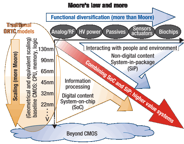
SiP growth is fueled by the fast-changing personal electronics market requiring smaller sizes, high performance and a platform capable of adapting quickly to changing chip technologies. Examples of current SiPs include radio frequency (RF) modules, which enjoy wide use in cell phones, and direct current (DC) power conditioning blocks. The 2009 ITRS has described the future SiP growth model under the title "more than Moore" [1]. In this vision, adding functionality with SiP technology leapfrogs traditional scaling approaches to accelerate time to market for tomorrow’s products (Fig. 1).
Click to Enlarge

Figure 1. System in package integration leapfrogs traditional scaling approaches, providing "More than Moore" functionality. SOURCE: Semiconductor Industry Association. The International Technology Roadmap for Semiconductors, 2009 Edition. SEMATECH, Austin, TX, 2009.

The success or failure of SIP designs depends upon the design, process, and test teams – wherever they are located – working together to ensure all components integrate well. These teams extend beyond an individual company to incorporate all the critical suppliers of the SiP. Often, establishing the team and inter-company relationships is the most difficult barrier to SiP integration. As SiPs become more complex, improved inter-company relationships will be increasingly important to successful design and fabrication. The following sections discuss specific challenges and technology choices team members must address.

Overcoming design complexities. As SiPs use devices from different sources, design data porting from different sources to the SiP design has become increasingly complex. This means custom design features are required, as well as a design process that must recognize the interactions between all components. For example, an optimum pad placement plan for a device slated for the usual single chip package may not translate to the SiP environment. Therefore a co-design approach to chip layout will create the best trade-offs between I/O locations, system performance, package complexity, and even cost. The co-design usually entails coordination between cross functional teams from all the component suppliers to ensure successful design. These tight inter-company interactions reduce surprises which may lead to product delays. When families of SiP solutions are developed, design decisions from the driver product can be used to produce design templates to speed future development.

An increasing need for thermal management. Chips with different maximum operating temperatures are often packaged together, and ever-increasing levels of integration drive higher thermal densities, which must be well managed in SiPs. The thermal design must optimize the system for the "weakest link" device, or the device with the lowest maximum operating temperature. Integration of non-Si technologies such as gallium nitride (GaN) or silicon carbide (SiC) into SiPs will allow much higher operating temperatures than traditional Si technologies. This will require not only partitioned heat sinking, but thermal isolation between devices operating at different temperatures. Integration of materials with different maximum temperature ranges within a package may also be needed.

Interconnection advancements. Through-silicon via (TSV) and other fine pitch interconnections such as copper (Cu) pillars are more sensitive to substrate planarity and warpage since the amount of solder that provides warpage tolerance during reflow is less. These interconnects require substrates that are dimensionally stable over a wide temperature range in order to make the solder joints. Current packaging materials and processes are essentially scaled versions of coarser pitch solder bump flip chip technologies. Improvement is ongoing to control warpage and surface roughness to enable finer pitch interconnects, but more advances are needed.

The industry is considering newer, temperature stable substrate materials, glasses, and other materials. Careful evaluation of the solder joint reliability is also needed because the small Cu tips in TSV and Cu pillar technologies are prone to completely dissolve and to produce metallurgies that are different from the well known Cu-solder systems. Similarly, non-solder interconnect systems, including conductive pastes and nano-metals, should be studied to enable next-generation interconnect schemes beyond solder-to-metal approaches. New challenges must be addressed to meet the requirements of emerging applications that can place special requirements on interconnections. For example, in medical applications for analysis of blood, etc., the sensor must be disposable; this requires temporary high density interconnections from sensor or MEMS to the SiP.

Reliability considerations. The development of portable sensors for temperature, humidity, chemical and biological species and ability to process and transmit data from local sites have opened up new applications for SiP "always-on" systems. These will drive the development of new high-temperature, moisture-resistant and chemical-resistant materials. Outdoor applications such as electronics for automobiles, base stations, to-the-house fiber optic connections, and solar panels have components exposed to the elements and need to be resistant to rain, atmospheric chemicals, and long term sunlight exposure. Additionally, low maintenance infrastructure applications must be able to operate reliability for extended periods such as 20-25 years. These harsh environment requirements are driving the need to better understand the link between failure modes accelerated by traditional package reliability tests and field failure modes.

Future directions

Optical chip-to-chip interconnects within a SiP are likely to gain prominence in the coming years, but integration of wave guides and coupling of wave guides to ICs are major challenges. Multiple research organizations are investigating solutions to switch optical signals within a package, distributing these signals through a 3D die stack, as well as from package to package. Glass substrates have emerged as a strong candidate for such applications [2].

Additionally, embedding passives and actives in the substrate enables even higher integration density in SiPs. With embedding, the passives or active chips are built into the substrate during the manufacturing process. As these chips become more complex, finer pitch interconnections for the substrate will be needed. The business model will increasingly involve engaging the substrate supplier to integrate multiple components of the final packaged product; hence, the substrate supplier will increasingly become a key participant in the overall design team for product success.

Conclusion

In summary, SiP solutions can enable even more novel electronic products with faster time to market than would be possible with traditional scaling. Proper up-front evaluation of SiP designs, having a tool box of enabling technologies, and coordination between all involved parties will be a critical requirement Many are working toward overcoming these challenges.

References

1. ITRS 2009. Executive Summary section, p. 10, and Assembly and Packaging section, pp. 21-22.

2. H. Schröder, L. Brusberg, R. Erxleben, I. Ndip, M. Töpper, N. F. Nissen, H. Reichl, "GlassPack – A 3D Glass Based Interposer Concept for SiP with Integrated Optical Interconnects," ECTC Conf. Proc., 2010.

Biographies

Darvin Edwards received his BS in physics from Arizona State U. and is a TI Fellow and Manager of SC Package Modeling and Simulation at Texas Instruments, 13020 TI Blvd., MS 3621, Dallas, TX 75243 USA; ph.: 214-567-3569; email: [email protected]

Masood Murtuza received his BTech in mechanical engineering from Indian Institute of Technology, Madras, India and an MSc from U. College, U. of London, UK, and is a TI Fellow in SC Packaging at Texas Instruments, Stafford, TX USA.

More Solid State Technology Current Issue Articles
More Solid State Technology Archives Issue Articles