Category Archives: LEDs

March 22, 2011 – BUSINESS WIRE — United LED Shan Dong Corp. (ULED), a China-based joint venture between United Microelectronics Corp (UMC) and Epistar, placed a multi-tool order for Veeco Instruments Inc. (Nasdaq: VECO) TurboDisc K465i metal organic chemical vapor deposition (MOCVD) systems. The systems will be installed at ULED’s facility in Jining City, China for its high-brightness light emitting diode (HB-LED) manufacturing ramp.

"The K465i provides the process performance and lowest cost of ownership needed to advance ULED’s position as a provider of LED devices for various lighting applications," said Dr. Tzu-Chi Wen, VP, Epi factory of United LED, commented.

Bill Miller, PhD, EVP, Compound Semiconductor and head of Veeco’s MOCVD Operations noted that the China LED sector is growing, and high yields are neccessary for competitiveness.

With high uniformity and run-to-run repeatability, the K465i suits high-volume LED manufacturing. The K465i provides ease-of-tuning for fast process optimization on wafer sizes up to 8" and fast tool recovery time after maintenance.

United LED Corporation, a joint venture between United Microelectronics Corp and Epistar, designs, manufactures, and sells Light Emitting Diodes (LED) chips. The company is based in Shandong, China.

Veeco makes equipment to develop and manufacture LEDs, solar panels, hard disk drives, and other devices. Visit www.veeco.com.

Subscribe to Solid State Technology/Advanced Packaging.

Follow Solid State Technology on Twitter.com via editors Pete Singer, twitter.com/PetesTweetsPW and Debra Vogler, twitter.com/dvogler_PV_semi.

Or join our Facebook group

March 21, 2011 — CEA-Leti and IPDiA have formed a common lab to capitalize on their complementary expertise in miniaturization and 3D integration on silicon.

The common lab is dedicated to developing new 3D-integration technologies for passive electronics components on silicon, targeting new applications in LED lighting, healthcare and aerospace that require extreme miniaturization. The partnership also will aim for improved miniaturization of passive components such as resistors, capacitors and inductors.

The common lab will develop very high-end passive components on silicon that will resist harsh environments, functional sub-mounts for lighting components, and assembly technologies that enable ultra-miniaturization of future products.

IPDiA was founded to commercialize innovative 3D technologies for integrating passive components. The company’s two axes of focus are integrated devices for high-brightness LEDs (HB-LEDs) and integrated passive devices (IPDs) for new medical, industrial, aerospace and defense markets.

CEA-Leti’s expertise in 3D technologies will allow IPDiA to go beyond the third generation of Passive Integration Connecting Substrate (PICS) components (250nF/mm2), which are being produced at IPDiA’s Caen site, and pursue the development of a future generation of PICS components (1µF/mm2, then 2µF/mm2) and their assembly. These products are designed, developed and manufactured by IPDiA in its production unit.

Franck Murray, CEO of IPDIA, pointed out that the Common Lab will entail "common work between teams from various backgrounds generating creativity and new ideas."

CEA-Leti and IPDIA have worked together since IPDIA formed in 2009.

CEA is a French research and technology organization, with activities in four main areas: energy, information technologies, healthcare technologies and defense and security. Within CEA, the Laboratory for Electronics & Information Technology (CEA-Leti) works with companies in order to increase their competitiveness through technological innovation and transfers. CEA-Leti is focused on micro and nanotechnologies. Visit www.leti.fr.

IPDiA is a leader in passive-components integration on silicon with a global offer for miniaturization that features high-level technological and economic performance. The company is mainly focused on healthcare, lighting, communication, defense, aerospace, industry and automotive. For more information, visit www.ipdia.com.

Subscribe to Solid State Technology/Advanced Packaging.

Follow Advanced Packaging on Twitter.com by clicking www.twitter.com/advpackaging. Or join our Facebook group

March 21, 2011 — The Optogan Group, Germany-based LED manufacturer, placed a multi-system order for Oxford Instruments’ etch and deposition systems. These include PlasmaPro System133 ICP and PlasmaPro 800Plus RIE etch systems, and a PlasmaPro 800Plus deposition system. 
 
The PlasmaPro System133 process tool offers up to 27 x 2" batch etch capability for GaN-on-sapphire wafers, while the PlasmaPro 800Plus tools are a flexible solution for plasma etching and deposition processes on large wafer batches of up to 43 x 2" wafers, in a compact footprint, open loading system.

The Optogan Group develops and produces high-brightness light emitting diodes (HB-LEDs) for global applications and ordered the systems for installation at its high-volume production manufacturing line in Landshut, Germany.
 
Optogan has operated an Oxford system for several years, and is now adding Oxford Instruments’ production systems for their large batch, high yield and high speed capabilities. Optogan cited high throughput, repeatability, and excellent local customer support as keys to the repeat order.

Oxford Instruments provides high technology tools and systems for industrial and research markets. It is listed on the London Stock Exchange (OXIG).

Oxford Instruments Plasma Technology offers flexible, configurable process tools and leading-edge processes for the precise, controllable and repeatable engineering of micro- and nano-structures. Its systems provide process solutions for nanometer-layer epitaxial growth of compound semiconductor material, etching of nanometer-sized features and the controlled growth of nanostructures. These solutions are based on core technologies in plasma-enhanced deposition and etch, ion-beam deposition and etch, atomic layer deposition and hydride vapor phase epitaxy.

The Optogan Group is one of the technology leaders in the manufacturing of light-emitting diodes (LEDs). Learn more at http://www.optogan.com

Subscribe to Solid State Technology/Advanced Packaging.

Follow Solid State Technology on Twitter.com via editors Pete Singer, twitter.com/PetesTweetsPW and Debra Vogler, twitter.com/dvogler_PV_semi.

Or join our Facebook group

March 21, 2011 — Bruker released the DektakXT stylus profiler, a production system with sustained repeatability of under 5 angstroms (<0.5nm).

The tenth generation of Dektak systems, DektakXT features a single-arch design with enhanced metrology features, a 64-bit parallel processing software architecture (Bruker’s Vision64 operating and analysis software, with access to over 200 distinct analyses), and a true-color HD camera.

The system performs nanometer-scale film thickness and surface texture measurements with improved gage repeatability and up to 40% faster scan performance. The new scanning subsystem and λ/10 optically flat reference enable improved baseline stability and the faster scan speeds. It offers low floor noise technology and integrated scalability.

DektakXT uses Dektak’s single sensor head design for optimum scanning flexibility and "Easy Tip Exchange" feature for rapid exchange of stylus tips to address a wide range of applications.

Widely used in microelectronics, semiconductor, display, solar, high-brightness LED, medical, scientific and materials science markets, Dektak stylus profilers are precision metrology instruments for production, research and failure analysis facilities. Dektak systems are used in 2D profilometry and 3D surface profiling applications to measure nanometer film thicknesses and step heights, 2D and 3D stress and other critical surface parameters that are vital in R&D, process development and Quality Assurance & Quality Control (QA/QC) applications.

DektakXT will be demonstrated in Bruker Booth 409 at the Society of Vacuum Coaters (SVC) TechCon 2011 in Chicago, IL, on April 19-20, 2011. For more information on DektakXT, or to schedule a demo or an appointment at SVC, contact Bruker at +1 (520) 741-1044 ext. 3, [email protected] or visit
www.bruker-axs.com.

Bruker Corporation provides high-performance scientific instruments and solutions for molecular and materials research, as well as for industrial and applied analysis. For more information about Bruker Corporation, please visit www.bruker.com.

Follow Small Times on Twitter.com by clicking www.twitter.com/smalltimes. Or join our Facebook group

March 18, 2011 – BUSINESS WIREIEEE, the technical professional association, announced it reached the 400,000 member mark for the first time in its history. By the end of 2010, total IEEE membership had surpassed 400,000, making it the seventh consecutive year the association had experienced membership growth.

Additionally in 2010, student membership reached 100,000 for the first time. The organization also experienced an overall increase in IEEE’s almost 40 technical society memberships over 2009, led by increases in communications, computer, and power and energy.

IEEE’s membership growth has occurred across the globe. On average, IEEE membership has been growing approximately 2% annually for the past seven years. Despite the economic environment, from 2008 to 2010 total IEEE membership increased 7% and student membership grew 21%.

IEEE Member and Geographic activities indicated that the membership performance is being driven by a robust integration of corporate and volunteer membership development initiatives, and an enhanced focus on the needs of each individual member.

In addition to membership growth, IEEE has also been expanding its operations globally. In late 2010, IEEE announced the opening of its first office in Bangalore, India and the relocation and expansion of its office in Singapore. Membership in the Asia Pacific region finished 2010 with more than 90,500 members, an increase of 65% since the year 2000.

IEEE is involved with highly cited publications, conferences, technology standards, and professional and educational activities. IEEE members are authorities on a wide variety of areas ranging from aerospace systems, computers and telecommunications to biomedical engineering, electric power and consumer electronics. Learn more at www.ieee.org

Subscribe to Solid State Technology/Advanced Packaging.

Follow Advanced Packaging on Twitter.com by clicking www.twitter.com/advpackaging. Or join our Facebook group

March 18, 2011 — Crossing Automation Inc., automation product and engineering services provider, introduced a new line of adaptive standard mechanical interface (SMIF) loadport (LPT) products for open cassette 200mm wafer process, metrology, and inspection tools.

The adaptive SMIF-LPT solutions offer cost-effective upgrades of non-SMIF tools to SMIF, thereby enabling the conversion of existing 200mm facilities for semiconductor manufacturing at technology nodes below 180nm.

The three new configurations are designed to address original equipment manufacturer (OEM) tool configurations with difficult cassette landing stages.

  • The SMIF-LPT Tr is a rotational head designed for non-perpendicular cassette placement.
  • The SMIF-LPT Tx offers a lateral cassette motion to address narrow cassette-to-cassette spacing.
  • The SMIF-LPT Ty has an offset arm to accommodate narrow chamber openings.

These new features can also be combined or upgraded on an existing SMIF-LPT. All of the adaptive SMIF solutions deliver improved particle performance to achieve Class 1 particle performance in a Class 100 clean room environment.

Crossing Automation supplies efficient, cost-effective vacuum and atmospheric automation solutions, materials tracking and engineering services to high volume semiconductor equipment manufacturers, IC, LED and solar manufacturers and other adjacent markets. Learn more at http://www.crossinginc.com.

Subscribe to Solid State Technology/Advanced Packaging.

Follow Solid State Technology on Twitter.com via editors Pete Singer, twitter.com/PetesTweetsPW and Debra Vogler, twitter.com/dvogler_PV_semi.

Or join our Facebook group

March 16, 2011 — The Ontario County Local Development Corp. has awarded a $75,000 matching grant to the College of Nanoscale Science and Engineering’s (CNSE) Smart System Technology & Commercialization Center of Excellence (STC), leveraging an additional $75,000 from STC to fund a site master plan for the 57-acre high-tech campus in Canandaigua, NY.

The site master plan, which will be developed by Bergmann Associates, will assist STC as it seeks to become a state-designated "shovel-ready" site, making it a more attractive location for nanotechnology companies looking to locate in Ontario County and the greater Rochester, NY region.

Integrated into CNSE in a partnership between 2 New York Centers of Excellence, STC provides advanced capabilities that enable computer chips to interface with electro-mechanical and biological devices. Leveraged by CNSE’s $7 billion enterprise, the combination gives New York State a global competitive advantage in the development and commercialization of smart system technologies.

"We are optimistic that the high-tech tenant companies based at CNSE’s STC will be expanding in the years to come, and we want to ensure that when those companies are ready, they have the ability and capacity to expand on the STC campus," said Ontario County Economic Developer Mike Manikowski. CNSE’s STC and Moser Baer Technologies have already announced a $20 million public-private partnership to develop the a pilot production line for organic light emitting diodes (OLEDs). Moser Baer Technologies is the United States-based subsidiary of Moser Baer India, Ltd. With its partnership with CNSE’s STC, Moser Baer Technologies is now poised to make its Canandaigua location its first US-based manufacturing operation producing the first OLED manufacturing line for lighting in the U.S.

Moser Baer currently has 9 employees on-site at STC, which will soon increase to 19, and the company expects to create more than 50 jobs by the end of 2012. The company is ramping up its OLED pilot line in space leased in the existing buildings at STC, where Moser Baer Technologies has received support through a Geneva Empire Zone designation. Once the pilot line is successful, it would be advantageous for Moser Baer Technologies to consider locating additional manufacturing capacity here.

"Any future expansion would require additional square footage, so we are very pleased to see Ontario County Local Development Corp. assisting in the planning for future development at this site," said David Newman, VP, Moser Baer Technologies. "Having a shovel-ready location within the tax parcel where we have Empire Zone designation would clearly be an additional incentive to our future growth at this location."

CNSE’s STC assists a variety of partners in industry and government in transitioning new technologies from concept to commercialization. Maintaining a 140,000-square-foot facility with over 25,000 square feet of cleanrooms for micro electro-mechanical systems (MEMS) fabrication and packaging, CNSE’s STC works with small-, medium- and large-sized companies to provide pilot prototyping, low-volume manufacturing and scalable manufacturing. Learn more at http://cnse.albany.edu/Home.aspx

For more information on Ontario County Economic Development programs, visit www.ontariocountydev.org.

Follow Small Times on Twitter.com by clicking www.twitter.com/smalltimes. Or join our Facebook group
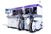
March 15, 2011 — KLA-Tencor Corporation (Nasdaq: KLAC), process control and yield management provider for semiconductor and related industries, introduced the ICOS CI-T620, a high-performance component inspector system for tape and reel.

Click to EnlargeAn addition to KLAC’s Component Inspector series, the CI-T620 is a fully automated optical inspector of integrated circuit (IC) packages for 3D measurements and package quality with dual tapers for improved output. Tape and reel is a process of packing surface mount devices by loading them into individual pockets within a pocket tape or carrier tape. The units are sealed in the carrier tape with a cover tape. The carrier tape is wound around a reel for handling and transport. The CI-T620 system has dual tapers working sequentially with minimal operator intervention to increase units per hour.
3D metrology inspection down to 5mm and high-resolution imaging capture surface defects down to 40µm. The system boasts faster package changeover (<5 minutes) and a throughput increase of up to 80%, compared to current industry methods. A complete portfolio of unique 2D and 3D inspection capabilities is supported by KLA-Tencor’s proprietary technology, and compatibility with a broad range of packages and sizes: 3 x 3mm to 42.5 x 42.5mm

KLA-Tencor’s component inspector system will be introduced at SEMICON China, taking place March 15-17 at the Shanghai Convention and Exhibition Center.

KLA-Tencor Corporation (NASDAQ: KLAC) provides process control and yield management products for the semiconductor, data storage, LED, photovoltaic, and other related nanoelectronics industries. Additional information may be found at www.kla-tencor.com.

Subscribe to Solid State Technology/Advanced Packaging.

Follow Advanced Packaging on Twitter.com by clicking www.twitter.com/advpackaging. Or join our Facebook group

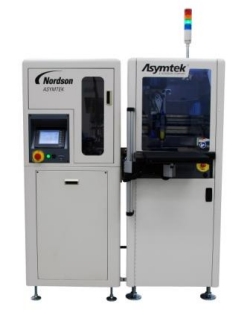
March 3, 2011 — Nordson ASYMTEK, dispensing, coating, and jetting technologies provider, introduced jet dispensing for manufacturing of side-view LEDs. The Spectrum S-920N fluid dispenser jets 0.1 to 0.2mm dots through windows as small as 0.4mm into LED cavities.

Click to EnlargeNordson ASYMTEK’s Spectrum S-920N jetting system automatically maintains a consistent shot weight with software-managed dispense parameters. Closed-loop dispensing eliminates operator adjustment. "Consistent dispensing weight improves process capability while ensuring higher units per hour," said Akira Morita, business development manager at Nordson ASYMTEK. "Using CPJ+ (calibrated process jetting plus), the process variability is reduced for tight LED color quality."

The system uses a jet for non-contact dispensing. Unlike a needle, the jet retracts much less for silicone break off and therefore shoots multiple shots faster, increasing speed and throughput. The jet’s small, controlled drops of fluid reach tight cavities consistently and reliably, unlike needles which have orifices larger than the cavity windows of side-view LEDs. Nordson ASYMTEK states that the system is easier to set up and maintain in production than multi-headed needle dispensing systems.

Side-view LEDs are incorporated into displays in tablet computers, smart phones, e-readers, and other devices. "As these LED devices get slimmer, the challenge to dispense specialized fluids, like silicone phosphor, into these tight spaces becomes greater," explained Morita.

View the free, on-demand webcast, "Light and Color Measurement of Today’s LED Technology" from Konica Minolta here.

Visit Nordson ASYMTEK at SEMICON China Booth 2437.

Nordson ASYMTEK provides precision automated fluid dispensing, conformal coating, and jetting technologies and designs and manufactures a full line of dispensing and coating systems. Nordson Corporation (Nasdaq: NDSN) is one of the world’s leading producers of precision dispensing equipment that applies adhesives, sealants, liquid and powder coatings and other materials to a broad range of consumer and industrial products during manufacturing operations. For more information, visit www.nordsonasymtek.com

Subscribe to Solid State Technology/Advanced Packaging.

Follow Advanced Packaging on Twitter.com by clicking www.twitter.com/advpackaging. Or join our Facebook group

March 1, 2011 – Business Wire — Nanometrics Incorporated (Nasdaq:NANO), advanced process control metrology provider, launched the Mosaic II turnkey image-based overlay metrology solution for advanced high-volume IC manufacturing. NANO reports an initial delivery to a leading Asian memory customer.

With the launch of the Mosaic II, Nanometrics supports advanced lithography process control, including double patterning processes used on today’s most advanced devices, commented David Doyle, vice president and business unit manager of Nanometrics. "We continue to strengthen our product offerings in this important market with a major Asian customer selecting the Mosaic II system for production line monitoring of their most challenging devices."

The Mosaic II is designed as part of Nanometrics’ Lynx cluster metrology platform, combining Mosaic II with IMPULSE modules onto a Lynx metrology cluster. This configuration would enable image-based overlay, diffraction-based overlay (DBO) and optical critical dimension (OCD) measurements. Earlier generation Caliper Mosaic tools can be field upgraded to Mosaic II capability.

To learn more about the Mosaic II, Lynx cluster metrology, and Nanometrics process control metrology solutions, visit Nanometrics at SPIE Advanced Lithography, San Jose Convention Center, through March 2 at Booth 324.
More SPIE news:

Nanometrics provides advanced, high-performance process control metrology systems used primarily in the fabrication of semiconductors, high-brightness LEDs, data storage devices and solar photovoltaics. Nanometrics’ website is http://www.nanometrics.com.


Copyright 2011 Business Wire

Subscribe to Solid State Technology/Advanced Packaging.

Follow Solid State Technology on Twitter.com via editors Pete Singer, twitter.com/PetesTweetsPW and Debra Vogler, twitter.com/dvogler_PV_semi.

Or join our Facebook group