Table of Contents
Solid State Technology
Year 2011
Issue 4
 | COLUMNS
Editorial
The Impact of Japan's Triple Disaster
Peter Singer, Editor-in-Chief
Industry Forum
Packaging Roadmaps at MEPTEC
Phil Garrou, Contributing Editor
|
|
DEPARTMENTS
World News.html
World News
Technology News
Metal organic precursors for LED manufacturing
At the Strategies in Light conference (Feb. 22-24, Santa Clara, CA), Ravi Kanjolia, CTO of SAFC Hitech, discussed metal organics (MO) supply issues and technologies being adopted by compound semiconductor manufacturers.
Technology News
SPIE 2011: Where are we now with EUV?
Given the mountainous expenditures in EUV lithography, what are its main accomplishments so far?
New Products.html
New Products
| |
Technology News
| |
FEATURES
Cover Article
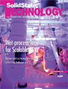
Wet-process technologies for scalable through-silicon vias
Electrografting nanotechnology has been optimized for highly conformal growth of TSV films, enabling a large reduction in cost-of-ownership per wafer compared to the dry process approach. Claudio Truzzi, Alchimer S.A., Massy, France
Wafer Cleaning Surface P
Surface preparation for 2011 and beyond
Surface clean engineers must discover new methods to realize contamination and surface termination requirements at each step of the manufacturing process, while simultaneously considering the impact to health, cost and the environment. Joel Barnett, SEMATECH, Austin, TX, USA
Wafer Cleaning Surface P
Random yield loss during wafer cleaning
The Cleaning studies of silicon wafers in DI water in both conventional wet-bath and a single-wafer cleaning tool clearly show that pumping methods have a strong influence on process performance. R. Prasanna Venkatesh, Jung-Soo Lim, Jin-Goo Part, Hanyany University, Ansan, Korea
| |
|