Table of Contents
Solid State Technology
Year 2009
Issue 5
 | COLUMNS
Editorial
In Search of the Next Switch
Jeff Welser, director of the Nanotechnology Research Initiative, is on a mission to find a replacement for the transistor, which is rapidly approaching fundamental limitations.
Tsv Reaps Headlines Mvp
TSV reaps headlines, MVP reaps profits
While high-density through-silicon vias (TSV) hold the limelight in advanced packaging development, a low-density via-through-pad version of TSV has moved past them to production.
Industry Forum
A PV manufacturing state of the union
Historically, photovoltaic (PV) manufacturers have developed in-house capability one machine at a time, and since the industry was small, there was little outside interest in changing this paradigm.
|
|
DEPARTMENTS
World News.html
World News
Tech News
Megasonic cleaning tool seeks a clean sweep at 65nm and below
At advanced technology nodes (65nm and below) there is a need for cleaning technology that better manages the ever-shrinking cleaning process window.
Tech News
New inspection tool addresses yield, solar cell classification
KLA-Tencor Corporations’s latest inspection product, the PVI-6, designed for optical in-line dual-sided inspection of photovoltaic (PV) wafers and cells, can inspect solar wafers and cells at the highest speed and accuracy for all stages of the production process, according to the company.
Tech News
Double-duty tool cuts costs for c-Si solar-cell wafering
The most expensive component of crystalline silicon-based PV manufacturing flow is the wafer — reducing wafer fabrication cost is considered key to the goal of making solar energy competitive with grid power.
Tech News
Parallel probing universes draw closer
For the most part, the universes of wafer probes and sockets have customarily been separate and distinct.
Product News.html
Product News
| |
FEATURES
Cover Article
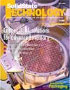
Copper BEOL solutions for advanced memory
While most copper back-end-of-line (BEOL) memory applications today utilize a single damascene layer of copper for the bitline, there are growing applications that utilize multiple copper layers and dual damascene.
The Reliability Margin O
The reliability margin of interconnects for advanced memory technologies
The trends of decreasing dimensions and new materials motivated the investigation of how these may affect the dielectric reliability of the interconnect structures.
Identifying Yield Impact
Identifying yield-impacting polishing-induced defects on polished silicon substrates
Traditional incoming wafer quality analysis methods have proven inadequate in detecting polishing induced defects (PID).
Thermal Laser Separation
Thermal laser separation for wafer dicing
Thermal laser separation (TLS) is used to separate brittle materials using well known basic principles.
| |
|