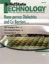
Table of Contents
Solid State Technology
Year 2011
Issue 5
 | FEATURES
Interconnect Structures
BEOL technology at 20nm half-pitch
New approaches to patterning, low-k and metallization are reviewed for 20nm hp interconnects. Gerald Beyer, Zsolt Tokei, imec, Leuven, Belgium
Redistribution Layers
RDL: an integral part of today's advanced packaging technologies
RDL technology has been instrumental in the development of many advanced packaging technologies such as fan-in and fan-out WLP, and TSV applications. Philip Garrou, MCNC, Research Triangle Park, NC; Alan Huffman, RTI Int., Research Triangle Park, NC
Next Genergation Ics
Pioneering new devices and materials for future ICs
It is expected that from the 15nm node on, the industry will need to adopt new transister architectures; among the contenders: FinFETs and TunnelFETs. Thomas Hoffmann, imec, Leuven, Belguim
Test Sockets
Configurable Kelvin contacting for today's advanced packages
In the precision analog marketplace Kelvin testing is becoming increasingly important to adequately test today's advanced packages. Jeff Sherry, Johnstech International, Minneapolis, MN USA
Cover Article
Nano-porous dielectrics and copper barriers for 28nm and below
Copper barrier solutions exist that ensure electrical and reliability performance even as device scaling continues. Harry Whitesell, Eric Hollar, Kang Sub Yim, Li-Qun Xia, Thamos Nowak, Applied Materials, Santa Clara, CA USA
|
|
COLUMNS
Editorial
A Day at CAMP
Peter Singer, Editor-in-Chief
Industry Forum
Millisecond annealing: extendible to 20nm and beyond
Jeff Hebb, Ultratech, Inc., San Jose, CA USA.
| |
DEPARTMENTS
World News.html
World News
Technology News
3D CT X-ray imaging fills inspection gaps, says Xradia
Xradia has unveiled its latest micro computed tomography (CT) 3D X-ray imaging system, the VersaXRM, targeting gaps in the semiconductor, materials science, geomaterials, and life sciences market segments.
Technology News
LED test standards, packaging material challenges
Emerging LED test standards and HB-LED packaging materials pros/cons were two of the topics covered at MEPTEC's The Heat is On event in late March.
Technology News
IBM to use water cooling for future 3D IC processors
At the recent CeBIT Fair in Hanover, Germany, IBM CEO Sam Palmisano announced that IBM's 3D technology will likely appear in its Power8 processor, planned for 2013, using 28nm or 22nm process technology.
Technology News
3D IC toolset readiness, Cu bonding, interposer failings
The recent IMAPS Global Business Council Meeting and Device Packaging Conference (mid-March in Ft. McDowell, AZ) was the source of some significant new developments in the areas of 3D IC and fan-out wafer-level packaging.
| |
|