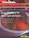
Table of Contents
Solid State Technology
Year 2009
Issue 4
 | COLUMNS
Editorial
Basic Research is Now Applied
The American Recovery and Reinvestment Act (HR 1), which was signed into law on February 17th by President Obama, includes more than $15 billion for vital scientific research programs.
Industry Forum
CMP grows a paunch
There’s no question about it. CMP is showing all the signs of middle age as it ambles past its quarter century milestone.
|
|
DEPARTMENTS
World News.html
World News
Tech News
The tightening litho horse race
Experts say we’re on an ‘optics forever’ path. EUV is gaining momentum and closing the gap, though the finish line is still several years away (and may keep moving).
Tech News
“Virtuous cycle” for ICs, LCD applies to PV too
Moore’s Law predicts the supply side of ICs, but the demand side can be understood as a “virtuous cycle” of technology advancement, lower costs, and rising demand leading to reinvestment.
Tech News
NEC: Trumping conventional scaling with 3D packaging
In a bid to expand applications for 3D packaging, NEC has developed a 3D chip-stacked flexible memory to support large-scale high-performance systems-on-chip (SoC).
Product News.html
Product News
| |
FEATURES
Cover Article
Precursors for group IV epitaxy for micro/opto-electronic applications
As device engineers are turning to material scientists to provide new materials for enhanced functionality of device platforms, the materials scientists are turning to chemists to provide new chemistries to realize novel functionality within the epitaxial deposition process.
Progress Towards The Mer
Progress towards the merger of compound semiconductors and silicon
Judging by the 2008 International Electron Device Meeting (IEDM), momentum continues to build toward eventual integration of compound semiconductors and mainstream silicon technology.
Automation Is Key To Get
Automation is key to getting lean for 450mm manufacturing
ISMI has been the leader in implementing small-lot manufacturing and single wafer processing for 300mm Prime and next-generation factory (NGF) 450mm manufacturing.
Deep Silicon Etch For Ts
Deep silicon etch for TSVs with improved via profile/process control
Through-silicon via (TSV) is an emerging technology for scaling, packaging, and continuing the drive to higher density and higher performance ICs.
Codesign Enables Rapid D
Codesign enables rapid development and high performance
The benefits of chip/package and chip/package/board codesign flows are realized only through early and frequent communications.
| |
|