Table of Contents
Solid State Technology
Year 2006
Issue 2
 | DEPARTMENTS
Editorial
The six billion dollar gap
Economists have been delivering dire warnings lately that the semiconductor industry will soon no longer be able to continue making IC devices smaller, faster, and cheaper at the same pace it has maintained over the past 40 years.
World News
World News
Tech News
Technology News
Compound Semiconductors
Fabricating buried tunnel junctions for InP-based VCSELs
Long-wavelength (λ≥1.3µm) vertical cavity surface emitting lasers (VCSEL) are highly attractive light sources for applications in optical communication and sensing.
Mems
Integrating MEMS devices using low-temperature wafer bonding
Long-term limitations of wafer bonding methods include surface roughness and substrate bow/warp considerations.
Lithography
Accuracy, speed, new physical phenomena: The future of litho simulation
Optical lithography modeling began in the early 1970s and represented the first serious attempt to describe lithography not as an art, but as a science.
Product News
Product News
Industry Forum
On entering a new era of product-driven technology
The international community expects a continuation of IC dimension scaling beyond the 22nm technology generation, with a technology node cycle of two to three years.
|
|
ITRS-SPECIAL-REPORT
Process Integration Devi
Trends and challenges in MOSFET scaling
As in previous editions, the 2005 edition of the International Technology Roadmap for Semiconductors (ITRS) [1] projects rapid scaling of the physical dimensions for leading-edge MOSFET transistors, with values of the physical gate length (Lg) under 10nm beyond 2015.
Frontend Processes
Frontend processes required for continued CMOS scaling
During the next several years, frontend processes will require the introduction of a variety of high-k materials and highly-engineered metal films for applications as diverse as MOSFET gate stacks, DRAM storage capacitors, and flash-memory storage devices.
Lithography
Many options expected in the future of lithography
The 2005 ITRS details the qualitative challenges associated with - and the quantitative requirements for - lithography using the incumbent projection imaging at 193nm wavelength with immersion lenses.
| |
FEATURES
Cover Article
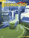
Advanced process control extends ECMP process consistency
ECMP provides greater control capabilities compared to CMP processes, and a multizone cathode allows for precise control over within-wafer uniformities.
| |
|