Table of Contents
Solid State Technology
Year 2005
Issue 8
 | DEPARTMENTS
Editorial
A node too far?
Debates about semiconductor engineering often focus on the physical limitations of building smaller and smaller transistors or mass-producing them on larger and larger wafers.
World News
World News
Tech News
Technology News
Interconnect
A novel technique for sealing porous dielectrics
As the industry moves toward the 45nm node and beyond, pore sealing is critical to enable the integration of porous low-k dielectric materials.
Materials
Coupling substrate and architecture with thin-layer transfer technology
Silicon-on-insulator (SOI) is the first example of an engineered substrate with an active top Si layer decoupled from the support wafer by the buried oxide (BOX), thereby addressing mainstream MOSFET performance requirements.
Product News
Product News
Perspectives
New materials - new business model?
Solid State Technology asked industry experts to comment on the pressures being exerted on the materials business model.
Online Staff Report
ConFab speakers debate the new economics of chipmaking
The ConFab — sponsored by Solid State Technology and our parent company, PennWell — brought together the leading semiconductor manufacturing executives for three days of dialogue and collaboration this past May in Las Vegas.
|
|
FEATURES
Lithography
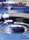
Stepping and scanning into the NA>1 immersion exposure era
During the past two years, immersion 193nm lithography has made astonishing strides in moving from the conceptual stage in R&D to the development and testing of the first full-field scanners that use water between the wafer and exposure lens to improve depth-of-focus (DOF) and printing resolution.
Wafer Cleaning
Single-tank processing demonstrates immersion batch cleaning for 65nm ICs
An advanced batch immersion system for wafer cleaning applications has been tested in 65nm pilot-line production.
Packaging Assembly
Advances in thick photoresists for flip-chip bumping
The push to smaller process geometries and higher-count I/O on ICs in portable and wireless applications has significantly increased the industry’s focus on chip-scale packaging and flip-chip assembly techniques, which deposit metal contact bumps across the entire surface of a die.
Software
A flexible ‘wrapper’ enables secure IP sharing
The growing need for collaboration in the semiconductor industry has created an additional challenge: protection of intellectual property (IP) while sharing capabilities in wafer fabs.
| |
ASIA-PACIFIC
Whatrsquos Next For Chin
What’s next for China’s emerging IC industry
This year’s significance for China’s electronics industry, and especially for its semiconductor segment, should not be underestimated.
Competing Fab Strategies
Competing fab strategies rely on advanced automation
No corner of the semiconductor industry is expanding manufacturing capacity faster than Asia, where rising competition between established players such as Taiwan and the emerging Chinese semiconductor industry are helping to drive growth.
New Demand And Challenge
New demand and challenges for gold-bump technology
Asia has been a dynamic region for the development and manufacturing of liquid-crystal display (LCD) panels.
| |
|