Table of Contents
Solid State Technology
Year 2000
Issue 8
 | DEPARTMENTS
Editorial
Design and chip fabrication need to be linked
In the digital design world there have long been two camps, often separated geographically and rarely in contact with each other. One is the design camp, full of banks of workstations ablaze with color-coded chip layouts; the designers follow a set of design rules supplied by the fab to avoid such flaws as too little space between traces.
World News
World News
Fab capacity utilization edges up as book-to-bill soars; Semi bookings steady at $2.75B in May; SEAJ sees strength with $1.6B in orders ...
Tech News
Technology News
Sandia researchers produce tiny canals on chips with new technique; ARS 2000 encourages maskmakers to share the value added ...
Eurofocus
Euro Focus
Mattson plans to acquire STEAG unit, CFM; BASF sees 20% shortfall in hydroxylamine supply; Philips to buy IBM MiCRUS fab ...
Asiafocus
Asia Focus
1st Silicon plans production ramp; S. Korea's Hyundai to concentrate on chip foundry business ...
Market Watch
SOC devices spur ASIC market
The application specific IC (ASIC) industry has received a great deal of attention over the past few years (probably second only to the highly volatile DRAM market).
People
People
Thomas Robert Rowbotham has been elected to the board of The Institute of Electrical and Electronics Engineers (IEEE) as divisional director. In this capacity, he will serve as liaison between the board and the IEEE Communications ...
New Literature
New Literature
FPD web site; Sealing technology web site; Seal application CD-ROM; Spectroscopic ellipsometer data sheets ...
New Products
New Products
Low-energy ion implant from Axcelis Technologies Inc.; Universal CMP system from SpeedFam-IPEC Inc.; High-speed defect detection system from Applied Materials Inc.; PECVD system for dielectric films from Novellus Systems Inc....
|
FEATURES
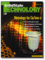
Metrology Test
Process development based on copper and low-k dielectric metrology
Copper and low-k processes require metrology using a variety of automated tools currently employed in the IC fab environment. Recent applications development work described here includes measurement of thin film properties with spectroscopic ellipsometry tools, etch depth measurement and CMP monitoring with high-resolution profilometers, resistivity measurements, and Cu contamination analysis with the corona-oxide-semiconductor technique.
Gas Handling
Intracavity laser spectroscopy for real-time trace gas detection
Although no technology should be viewed as a panacea, intracavity laser spectroscopy trace gas sensors do provide a significant advance in measurement capabilities. They are particularly applicable for demanding, industry-leading applications in semiconductor manufacturing such as in situ gas monitoring, where rapid decision making is required during processing.
Industry Insights
Moore's Law switching to a subwavelength track
A huge transition from above-wavelength to subwavelength design and manufacturing is taking place in the semiconductor industry. Subwavelength features leave little margin for equipment error, making it difficult or impossible to control the critical dimensions of a process.
Contamination Control
Applying an electric field to control metals in furnaces
Despite intuition, application of an electric field does have a measurable effect on the movement of metallic contaminants in gas in a wafer processing thermal process. Research has shown that the phenomenon of positive surface ionization can give rise to significant electric field effects on the gas-phase transport of ionizable atoms such as alkali metals, even at very low fractional ionizations and modest electric fields.
Lithography
Chemistry and physics of the PEB process in a CA resist
Measurements and modeling of the post-exposure bake process of a chemically amplified resist reveal that diffusion plays little role and that the observed spreading of exposed regions results primarily from chemical kinetics in regions where a photo-acid gradient exists.
Analysis of volatile products during PEB reveals new side-reaction pathways.
Lithography
Beneath the MEEF
The effects responsible for enhancing small photomask CD errors are the same as those which narrow the exposure latitude. Innovations that increase the process window also reduce the mask error enhancement factor, thus doubly improving yield.
Lithography
Applying a thin imaging resist system to substrates with topography
A bilayer resist system consisting of a thin, silicon-containing imaging layer over a planarizing, reflection-suppressing underlayer gives better patterning performance than a single-layer resist/thin antireflective coating system, especially in dual-damascene applications with high topography.
Vacuum Technology
Using partial pressure analysis to monitor wet clean recovery
In general, when a fault in a vacuum system occurs, particularly after wet cleaning, it is usually the troubleshooting that takes the largest amount of time. Equipping the troubleshooter with a partial pressure analyzer, however, provides an effective tool for accelerating the troubleshooting process and, hence, accelerating corrective action. This tool can be an effective means for productivity enhancement of vacuum process tools.
|