Table of Contents
Solid State Technology
Year 2001
Issue 8
 | ASIA-PACIFIC
News
News
Asuka project to select tools this year; Ebara steps up technology development, plans US push; China: The sleeping dragon stirs.
Foundry Watch
Slow business doesn't discourage Asia's silicon foundries
Just over a year ago, foundry manufacturing epitomized the leading edge of semiconductor manufacturing technology, and Asia was the hotbed of foundry building activity. Has this changed? Leading executives comment on how the industry downturn in 2001 has affected Asia's silicon wafer foundries, particularly their business levels and building plans.
Taiwan
Bringing a new fab on-line: How TSMC Fab 6 got up and running
In today's economy, only the largest semiconductor companies can profitably operate their own fabs. As a result, smaller "fabless" firms rely on foundries to manufacture their products, and many larger companies are also moving to a business model in which entire product lines are strategically outsourced to foundry companies.
China
Amkor's experiences with factory opportunities in China
Microelectronics manufacturer Amkor Technology has successfully developed business relations in China that quickly led to manufacturing facilities. With discussion beginning less than a year ago, Amkor is now operating its 150,000 square foot facility in the Waigaoqiao Free Trade Zone near Pu Dong.
China
Experience and expectations when investing in Western China
Semiconductor manufacturer ON Semiconductor learned from its business relations with China's Leshan Radio and established a facility in China's Chengdu-Leshan area. This relationship has resulted in local government's sharing in the enthusiasm for a manufacturing facility, often going the extra mile necessary to smooth the path.
|
|
DEPARTMENTS
Editorial
Economics will dictate the future
It takes more and more investment to produce each generation of microchips in the march along the Moore's Law semi-log curve. While chip functions get steadily cheaper, and shrinking features allow more functionality and performance on each chip, the tools and fabs to manufacture them escalate in price.
World News
World News
Worldwide Highlights; USA; Japan; Europe; Asia Pacific ...
Tech News
Technology News
New technology tackles maskmaking challenges; Patented IC measures time to trillionths of a second...
Show Report
Cycle time, 300mm in spotlight at automation conference
Case studies and the migration to 300mm in the automation segment took center stage at the first Worldwide Automation & Performance Symposium, held in Salt Lake City, UT, and sponsored by Brooks Automation, Chelmsford, MA.
Asia Pacific
Singapore pours it on even in rough waters
Singapore has endured its fair share of economic hardships during this downturn, but instead of running for cover, the island nation is forging full steam ahead while weathering the latest storm.
Market Watch
Long-term market outlook may shine for OLED displays
Organic light-emitting diode (OLED) technology used in color displays that feature excellent image quality, especially in contrast and brightness, is generating big interest in the display sector and across the world of electronics.
Calendar
Calendar
A listing of industry events, covering August to November 2001.
New Products
New Products
Defect inspection for 300mm wafers; High-current implanter for 300mm; 300mm metallization; Mask aligner for 300mm...
Literature
Literature
Ionization booklet; Dispense and assembly web site; XRF technology guide; Assembly and rework application bulletins.
| |
FEATURES
Cover Article
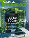
Factors in determining COO for 300mm FOUPs
300mm fabs are being planned and built with an unprecedented degree of automation. Wafer carriers for 300mm —front opening unified pods or FOUPs —are no longer inert pieces of plastic. They are small machines that must operate with each and every process tool in a 300mm fab.
Lithography
Plasma etch rates: The impact of mask transmittance
Plasma systems with endpoint detection are typically used to etch polysilicon and metal [1]. Etch rate depends on the exposed area ("loading effect"). If this dependence is neglected, severe physical variations of nominal etching conditions may occur at the wafer level, resulting in poor statistical process control of minimum-size patterns.
Lithography
The impact of airborne molecular bases on DUV photoresists
Over the past five years, the semiconductor industry has undergone numerous changes with the advent of 0.25µm geometries. Exposure tools have moved from i-line to deep ultraviolet (DUV), and a new vocabulary containing words like chemically amplified, photo-acid generator, T-topping, and molecular bases has become part of the process engineer's jargon.
Thermal Processing
An evaluation of semiconductor-grade polysilicon furnace fixtures
Data show that polysilicon furnace fixtures can significantly reduce post-LPCVD process particle counts and the need for periodic furnace fixture cleaning, and increase wafer deposition rate. Thermal and purity characteristics of this material also help to reduce defect densities and metallic contamination on silicon wafers. These data have been developed from long-term evaluations at many major semiconductor manufacturers.
Effluent Treatment
Chemistry and treatment of III-V semiconductor wastewater
Viable treatment and removal of contaminants from compound semiconductor fab operations require some familiarity with the aqueous chemistry of III-V elements (i.e., GaAs) on the periodic table. This knowledge will enable foundries and fabs to comply with local discharge limits and EPA regulations governing the semiconductor industry.
Semiconductor Assembly
Laser marking study proves benefits of simulation for backend tools
Researchers have developed a simulation model for an integrated laser marking machine and studied the effect of changes in a key system component on the manufacturing performance of the machine. The broader benefit from this work, specific to an integrated laser marking system, is that discrete event simulation is the best method for identifying the most effective settings in a specific manufacturing environment.
Industry Insights
In the age of 300mm silicon, tech standards are even more crucial
Technical standards are at work everywhere, from the IO of laptop computers to cell phones, from automobile tires to printer's paper. These standards are of two types: "voluntary" standards and those imposed by government regulatory agencies. Building codes and OSHA regulations (in the US) are representative of the latter.
| |
|