Tag Archives: AI

DAVE LAMMERS, contributing editor

Judging by the presentations at the 2018 Symposium on VLSI Technology, held in Honolulu this summer, the semiconductor industry has a challenge ahead of it: how to develop the special low-power hardware needed to support artificial intelligence-enabled networks.

To meet society’s needs for low-power-consumption machine learning (ML), “we do need to turn our attention to this new type of computing,” said Naveen Verma, an associate professor of electrical engineering at Princeton University.”

While introducing intelligence into engineering systems has been what the semiconductor industry has been all about, Verma said machine learning represents a “quite distinct” inflection point. Accustomed as it is to fast-growing applications, machine learning is on a growth trajectory that Verma said is “unprecedented in our own industry” as ML algorithms have started to outperform human capabilities in a wide variety of fields.

Faster GPUs driven by Moore’s Law, and combining chips in packages by means of heterogenous computing, “won’t be enough as we proceed into the future.  I would suggest we need to do something more, get engaged more deeply, affecting things done at all levels.”

Naresh Shanbhag, a professor at the University of Illinois at Urbana-Champaign, sounded a similar appeal at the VLSI symposium’s day-long workshop on machine learning. The semiconductor industry has taken a “back seat to the systems and algorithm researchers who are driving the AI revolution today,” he said.

Addressing several hundred device and circuit researchers, Shanbhag said their contributions to the AI revolution have been hampered by a self-limiting mindset,  based on “our traditional role as component providers.”

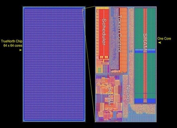
Until last year, Shanbhag served as the director of a multi-university research effort, Systems on Nanoscale Information fabriCs (SONIC, www.sonic-center.org), which pursued new forms of low-power compute networks, including work on fault-tolerant computing. At the VLSI symposium he spoke on Deep In-Memory Architectures and other non-traditional approaches.

“Traditional solutions are running out of steam,” he said, noting the slowdown in scaling and the the “memory wall” in traditional von Neumann architectures that contributes to high power consumption. “We need to develop a systems-to-devices perspective in order to be a player in the world of AI,” he said.

Stanford’s Boris Murmann: mixed-signal for Edge devices

Boris Murmann, an associate professor in the Department of Electrical Engineering at Stanford University, described a low-power approach based on mixed signal-based processing, which can be tightly coupled to the sensor front-end of small-form-factor applications, such as an IoT edge camera or microphone.

“What if energy is the prime currency, how far can I push down the power consumption?” Murmann asked. By coupling analog-based computing to small-scale software macros, an edge camera could be awakened by a face-recognition algorithm. The “wake-up triggers” could alert more-powerful companion algorithms, in some cases sending data to the cloud.

Showing a test chip of mixed-signal processing circuits, Murmann said the Stanford effort “brings us a little bit closer to the physical medium here. We want to exploit mixed-signal techniques to reduce the data volume, keeping it close to its source.” In addition, mixed-signal computing could help lower energy consumption in wearables, or in convolutional neural networks (CNNs) in edge IoT devices.

In a remark that coincided with others’ views, Murmann said “falling back to non-deep learning techniques can be advantageous for basic classification tasks,” such as wake-up-type alerts. “There exist many examples of the benefits of analog processing in non-deep learning algorithms,” he said.

MIT’s Vivienne Sze: CNNs not always the best

That theme – when deep learning competes with less power-hungry techniques – was taken up by Vivienne Sze, an associate professor at the Massachusetts Institute of Technology. By good fortune, Sze recently had two graduate students who designed similar facial recognition chips, one based on the Histograms of Oriented Gradients (HOG) method of feature recognition, and the other using the MIT-developed Eyeriss accelerator for CNNs (eyeriss.mit.edu). Both chips were implemented in the same foundry technology, with similar logic and memory densities, and put to work on facial recognition (FIGURE 1).

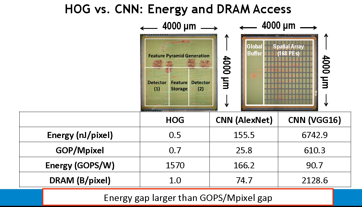
FIGURE 1. Two image processing chips created at M.I.T. resulted in sharply different energy consumption levels. Machine learning approaches, such as CNNs, are flexible, but often not as efficient as more hard-wired solutions. (Source: 2018 VLSI Symposium).

Calling it a “good controlled experiment,” Sze described the energy consumption versus accuracy measurements, concluding that the Eyeriss machine-learning chip was twice as accurate on the AlexNet benchmark. However, that doubling in accuracy came at the price of a 300-times multiplier in energy, increasing to a 10,000-times energy penalty in some cases, as measured in nanojoules per pixel.

“The energy gap was much larger than the throughput gap,” Sze said. The Eyeriss CNNs require more energy because of the programmability factor, with weights of eight bits per pixel. “The question becomes are you willing to give up a 300x increase in energy, or even 10,000x, to get a 2X increase in accuracy? Are you willing to sacrifice that much battery life?”

“The main point — and it is really important — is that CNNs are not always the best solution. Some hand-crafted features perform better,” Sze said.

Two European consortia, CEA-Leti and Imec, were well represented at the VLSI symposium.

Denis Dutoit, a researcher at France’s CEA Tech center, described a deep learning core, PNeuro, designed for neural network processing chains.

The solution supports traditional image processing chains, such as filtering, without external image processing. The modular SIMD architecture can be sized to fit the best area/performance per application.

Dutoit said the energy consumption was much less than that of traditional cores from ARM and Nvidia on a benchmark application, recognizing faces from a database of 18,000 images at a recognition rate of 97 percent.

GPUs vs custom accelerators

The sharp uptake of AI in image and voice recognition, navigation systems, and digital assistants has come in part because the training cycles could be completed efficiently on massively parallel architectures, i.e., GPUs, said Bill Dally, chief scientist at Nvidia Inc. Alternatives to GPUs and CPUs are being developed that are faster, but less flexible. Dally conceded that creating a task-specific processor might result in a 20 percent performance gain, compared with a GPU or Transaction Processing Unit (TPU). However, “you would lose flexibility if the algorithm changes. It’s a continuum: (with GPUs) you give up a little efficiency while maximizing flexibility,” Dally said, predicting that “AI will dominate loads going forward.”

Joe Macri, a vice president at AMD, said that modern processors have high-speed interfaces with “lots of coherancy,” allowing dedicated processors and CPUs/GPUs to used shared memory. “It is not a question of an accelerator or a CPU. It’s both.”

Whether it is reconfigurable architectures, hard-wired circuits, and others, participants at the VLSI symposium agreed that AI is set to change lives around the globe. Macri pointed out that only 20 years ago, few people carried phones. Now, no one would even think of going out with their smart phone – it has become more important than carrying a billfold or purse, he noted. Twenty years from now, machine learning will be embedded into phones, homes, and factories, changing lives in ways few of us can foresee.

PETE SINGER, Editor-in-Chief

The exploding use of Artificial Intelligence (AI) is ushering in a new era for semiconductor devices that will bring many new opportunities but also many challenges. Speaking at the AI Design Forum hosted by Applied Materials and SEMI during SEMICON West in July, Dr. John E. Kelly, III, Senior Vice President, Cognitive Solutions and IBM Research, talked about how AI will dramatically change the world. “This is an era of computing which is at a scale that will dwarf the previous era, in ways that will change all of our businesses and all of our industries, and all of our lives,” he said. “This is the era that’s going to power our semiconductor industry forward. The number of opportunities is enormous.”

Also speaking at the event, Gary Dickerson, CEO of Applied Materials, said AI “needs innovation in the edge and in the cloud, in generating data on the edge, storing the data, and processing that data to unlock the value.  At the same time Moore’s Law is slowing.” This creates the “perfect opportunity,” he said.

Ajit Manocha, President and CEO of SEMI, calls it a “rebirth” of the semiconductor industry. “Artificial Intelligence is changing everything – and bringing semiconductors back into the deserved spotlight,” he notes in a recent article. “AI’s potential market of hundreds of zettabytes and trillions of dollars relies on new semiconductor architectures and compute platforms. Making these AI semiconductor engines will require a wildly innovative range of new materials, equipment, and design methodologies.”

”Hardware is becoming sexy again,” said Dickerson. “In the last 18 months there’s been more money going into chip start ups than the previous 18 years.” In addition to AI chips from traditional IC companies such as Intel and Qualcomm, more than 45 start-ups are working to develop new AI chips, with VC investments of more than $1.5B — at least five of them have raised more than $100 million from investors. Tech giants such as Google, Facebook, Microsoft, Amazon, Baidu and Alibaba are also developing AI chips.

Dickerson said having the winning AI chip 12 months ahead of anyone else could be a $100 billion opportunity. “What we’re driving inside of Applied Materials is speed and time to market. What is one month worth?  What is one minute worth?”

IBM’s Kelly said there’s $2 trillion of decision support opportunity for artificial intelligence on top of the existing $1.5-2 billion information technology industry. “Literally every industry in the world is going to be impacted and transformed by this,” he said.

AI needed to analyze unstructured data

Speaking at an Applied Materials event late last year during the International Electron Devices Meeting, Dr. Jeff Welser, Vice President and Director of IBM Research’s – Almaden lab, said the explosion in AI is being driven by the need to process vast amounts of unstructured data, noting that in just two days, we now generate as much data as was generated in total through 2003. “Somewhere around 2020, the estimate is maybe 50 zettabytes of data being produced. That’s 21 zeros,” he said.

Welser noted that 80% of all data is unstructured and growing 15 times the rate of structured data. “If you look at the growth, it’s really in a whole different type of data. Voice data, social media data, which includes a lot of images, videos, audio and text, but very unstructured text,” he said. And then there’s data from IoT-connected sensors.

There are various ways to crunch this data. CPUs work very well for structed floating point data, while GPUs work well for AI applications – but that doesn’t mean people aren’t using traditional CPUs for AI.  In August, Intel said it sold $1 billion of artificial intelligence processor chips in 2017. Reuters reported that Navin Shenoy, its data center chief, said the company has been able to modify its CPUs to become more than 200 times better at artificial intelligence training over the past several years. This resulted in $1 billion in sales of its Xeon processors for such work in 2017, when the company’s overall revenue was $62.8 billion. Naveen Rao, head of Intel’s artificial intelligence products group, said the $1 billion estimate was derived from customersthat told Intel they were buying chips for AI and from calculations of how much of a customer’s data center is dedicated to such work.

Custom hardware for AI is not new. “Even as early as the ‘90s, they were starting to play around with ASICS and FPGAs, trying to find ways to do this better,” Welser said. Google’s Tensor Processing Unit (TPU), introduced in 2016, for example, is a custom ASIC chip built specifically for machine learning applications, allowing the chip to be more tolerant of reduced computational precision, which means it requires fewer transistors per operation.

It really was when the GPUs appeared in the 2008-2009 time period when people realized that in addition to the intended application – graphics processing – they were really good for doing the kind of math needed for neural nets. “Since then, we’ve seen a whole bunch of different architectures coming out to try to continue to improve our ability to run the neural net for training and for inferencing,” he said.

AI works by first “training” a neural network where weights are changed based on the output, followed by an “inferencing” aspect where the weights are fixed. This may mean two different kinds of chips are needed. “If you weren’t trying to do learning on it, you could potentially get something that’s much lower power, much faster, much more efficient when taking an already trained neural net and running it for whatever application. That turns out to be important in terms of where we see hardware going,” he said.

The problem with present day technology – whether it’s CPUs, GPUs, ASICs or FPGAs — is that there is still a huge gap between what processing power is required and what’s available now. “We have a 1,000x gap in performance per watt that we have to close,” said Applied Materials’ Dickerson.

There’s a need to reduce the amount of power used in AI processors not only at data centers, but for mobile applications such as automotive and security where decisions need to be made in real time versus in the cloud. This also could lead to a need for different kinds of AI chips.

An interesting case in point: IBM’s world-leading Summit supercomputer, employs 9,216 IBM processors boosted by 27,648 Nvidia GPUs – and takes a room the size of two tennis courts and as much power as a small town!

New approaches

To get to the next level in performance/Watt, innovations being researched at the AI chip level include:

  • low precision computing
  • analog computing
  • resistive computing

In one study, IBM artificially reduced the precision in a neural net and the results were surprising. “We found we could get down the floating point to 14 bit, and we really were getting exactly the same precision as you could with 16 bit or 32 bit or 64 bit,” Welser said. “It didn’t really matter at that point.”

This means that some parts of the neural net could be high precision and some parts that are low precision. “There’s a lot of tradeoffs you can make there, that could get you lower power or higher performance for that power, by giving up precision,” Welser said.

Old-school analog computing has even lower precision but may be well suited to AI. “Analog computing was extremely efficient at the time, it’s just you can’t control the errors or scale it in any way that makes sense if you’re trying to do high precision floating point,” Welser said. “But if what you really want is the ability to have a variable connection, say to neurons, then perhaps you could actually use an analog device.”

Resistive computing is a twist on analog computing that has the added advantage of eliminating the bottleneck between memory and compute. Welser said to think of it as layers of neurons, and the connections between those neurons would be an analog resistive memory. “By changing the level of that resistive memory, the amount of current that flows between one neuron and the next would be varied automatically. The next neuron down would decide how it’s going to fire based on the amount of current that flowed into it.

IBM experimented with phase change memory for this application. “Obviously phase change memory can go to a low resistance or a high resistance (i.e., a 1 or a 0) but there is no reason you can’t take it somewhere in between, and that’s exactly what we would want to take advantage of here,” Welser said.

“There is hope for taking analog devices and using them to actually be some of the elements and getting rid of the bottleneck for the memory as well as getting away from the precision/power that goes on with trying to get to high precision for those connections,” he added.

A successful resistive analog memory ultimately winds up being a materials challenge. “We’d like to have like a thousand levels for the storage capacity, and we’d like to have a very nice symmetry in turning it off and on, which is not something you’d normally think about,” Welser said. “One of the challenges for the industry is to think about how you can get materials that fit these needs better than just a straight memory of one bit on or off.”

Sundeep Bajikar, head of market intelligence at Applied Materials, writing in a blog, said “addressing the processor-to-memory access and bandwidth bottleneck will give rise to new memory architectures for AI, and could ultimately lead to convergence between logic and memory manufacturing process technologies. IBM’s TrueNorth inference chip (FIGURE 1) is one such example of a new architecture in which each neuron has access to its own local memory and does not need to go off-chip to access memory. New memory devices such as ReRAM, FE-RAM and MRAM could catalyze innovation in the area of memory-centric computing. The traditional approach of separating process technologies for high-performance logic and high-performance memory may no longer be as relevant in a new AI world of reduced precision computing.”

FIGURE 1. IBM’s TrueNorth Chip.

Editor’s Note: This article originally appeared in the October 2018 issue of Solid State Technology. 

Tom Ho and Stewart Chalmers, BISTel, Santa Clara, CA

Traditional FDC systems collect data from production equipment, summarize it, and compare it to control limits that were previously set up by engineers. Software alarms are triggered when any of the summarized data fall outside of the control limits. While this method has been effective and widely deployed, it does create a few challenges for the engineers:

  • The use of summary data means that (1) subtle changes in the process may not be noticed and (2) the unmonitored section of the process will be overlooked by a typical FDC system. These subtle changes or the missed anomalies in unmonitored section may result in critical problems.
  • Modeling control limits for fault detection is a manual process, prone to human error and process drift. With hundreds of thousandssensors in a complex manufacturing process, the task of modeling control limits is extremely time consuming and requires a deep understanding of the particular manufacturing process on the part of the engineer. Non-optimized control limits result in misdetection: false alarms or missed alarms.
  • As equipment ages, processes change. Meticulously set control limit ranges must be adjusted, requiring engineers to constantly monitor equipment and sensor data to avoid false alarms or missed real alarm.

Full sensor trace detection

A new approach, Dynamic Fault Detection (DFD) was developed to address the shortcomings of traditional FDC systems and save both production time and engineer time. DFD takes advantage of the full trace from each and every sensor to detect any issues during a manufacturing process. By analyzing each trace in its entirety, and running them through intelligent software, the system is able to comprehensively identify potential issues and errors as they occur. As the Adaptive Intelligence behind Dynamic Fault Detection learns each unique production environment, it will be able to identify process anomalies in real time without the need for manual adjustment from engineers. Great savings can be realized by early detection, increased engineer productivity, and containment of malfunctions.

DFD’s strength is its ability to analyze full trace data. As shown in FIGURE 1, there are many subtle details on a trace, such as spikes, shifts, and ramp rate changes, which are typically ignored or go undetected by a traditional FDC systems, because they only examine a segment of the trace- summary data. By analyzing the full trace using DFD, these details can easily be identified to provide a more thorough analysis than ever before.

Dynamic referencing

Unlike traditional FDC deployments, DFD does not require control limit modeling. The novel solution adapts machine learning techniques to take advantage of neighboring traces as references, so control limits are dynamically defined in real time.  Not only does this substantially reduce set up and deployment time of a fault detection system, it also eliminates the need for an engineer to continuously maintain the model. Since the analysis is done in real time, the model evolves and adapts to any process shifts as new reference traces are added.

DFD has multiple reference configurations available for engineers to choose from to fine tune detection accuracy. For example, DFD can 1) use traces within a wafer lot as reference, 2) use traces from the last N wafers as reference, 3) use “golden” traces as reference, or 4) a combination of the above.

As more sensors are added to the Internet of Things network of a production plant, DFD can integrate their data into its decision-making process.

Optimized alarming

Thousands of process alarms inundate engineers each day, only a small percentage of which are valid. In today’s FDC systems, one of the main causes for false alarms is improperly configured Statistical Process Control (SPC) limits. Also, typical FDC may generate one alarm for each limit violation resulting in many alarms for each wafer process. DFD implementations require no control limits, greatly reducing the potential for false alarms.  In addition, DFD is designed to only issues one alarm per wafer, further streamlining the alarming system and providing better focus for the engineers.

Dynamic fault detection use cases

The following examples illustrate actual use cases to show the benefits of utilizing DFD for fault detection.

Use case #1End Point Abnormal Etching

In this example, both the upper and lower control limits in SPC were not set at the optimum levels, preventing the traditional FDC system from detecting several abnormally etched wafers (FIGURE 2).  No SPC alarms were issued to notify the engineer.

On the other hand, DFD full trace comparison easily detects the abnormality by comparing to neighboring traces (FIGURE 3).  This was accomplished without having to set up any control limits.

Use case #2 – Resist Bake Plate Temperature

The SPC chart in Figure 4 clearly shows that the Resist bake plate temperature pattern changed significantly; however, since the temperature range during the process never exceeded the control limits, SPC did not issue any alarms.

When the same parameter was analyzed using DFD, the temperature profile abnormality was easily identified, and the software notified an engineer (FIGURE 5).

Use case #3 – Full Trace Coverage

Engineers select only a segment of sensor trace data to monitor because setting up SPC limits is so arduous. In this specific case, the SPC system was set up to monitor only the He_Flow parameter in recipe step 3 and step 4.  Since no unusual events occurred during those steps in the process, no SPC alarms were triggered.

However, in that same production run, a DFD alarm was issued for one of the wafers. Upon examination of the trace summary chart shown in FIGURE 6, it is clear that while the parameter behaved normally during recipe step 3 and step 4, there was a noticeable issue from one of the wafers during recipe step 1 and step 2.  The trace in red represents the offending trace versus the rest of the (normal) population in blue. DFD full trace analysis caught the abnormality.

Use case #4 – DFD Alarm Accuracy

When setting up SPC limits in a conventional FDC system, the method of calculation taken by an engineer can yield vastly different results. In this example, the engineer used multiple SPC approaches to monitor parameter Match_LoadCap in an etcher. When the control limits were set using Standard Deviation (FIGURE 7), a large number of false alarms were triggered.   On the other hand, zero alarms were triggered using the Mean approach (FIGURE 8).

Using DFD full trace detection eliminates the discrepancy between calculation methods. In the above example, DFD was able to identify an issue with one of the wafers in recipe step 3 and trigger only one alarm.

Dynamic fault detection scope of use

DFD is designed to be used in production environments of many types, ranging from semiconductor manufacturing to automotive plants and everything in between. As long as the manufacturing equipment being monitored generates systematic and consistent trace patterns, such as gas flow, temperature, pressure, power etc., proper referencing can be established by the Adaptive Intelligence (AI) to identify abnormalities. Sensor traces from Process of Record (POR) runs may be used as starting references.

Conclusion

The DFD solution reduces risk in manufacturing by protecting against events that impact yield.  It also provides engineers with an innovative new tool that addresses several limitations of today’s traditional FDC systems.  As shown in TABLE 1, the solution greatly reduces the time required for deployment and maintenance, while providing a more thorough and accurate detection of issues.


TABLE 1
  FDC

(Per Recipe/Tool Type)

DFD

(Per Recipe/Tool Type)

FDC model creation 1 – 2 weeks < 1 day
FDC model validation and fine tuning 2 – 3 weeks < 1 week
Model Maintenance Ongoing Minimal
Typical Alarm Rate 100-500/chamber-day < 50/chamber-day
% Coverage of Number of Sensors 50-60% 100% as default
Trace Segment Coverage 20-40% 100%
Adaptive to Systematic Behavior Changes No Yes

TOM HO is President of BISTel America where he leads global product engineer and development efforts for BISTel.  [email protected].   STEWART CHALMERS is President & CEO of Hill + Kincaid, a technical marketing firm. [email protected].

Editor’s Note: This article was originally published in the October 2018 issue of Solid State Technology.