
PETE SINGER, Editor-in-Chief
The exploding use of Artificial Intelligence (AI) is ushering in a new era for semiconductor devices that will bring many new opportunities but also many challenges. Speaking at the AI Design Forum hosted by Applied Materials and SEMI during SEMICON West in July, Dr. John E. Kelly, III, Senior Vice President, Cognitive Solutions and IBM Research, talked about how AI will dramatically change the world. “This is an era of computing which is at a scale that will dwarf the previous era, in ways that will change all of our businesses and all of our industries, and all of our lives,” he said. “This is the era that’s going to power our semiconductor industry forward. The number of opportunities is enormous.”
Also speaking at the event, Gary Dickerson, CEO of Applied Materials, said AI “needs innovation in the edge and in the cloud, in generating data on the edge, storing the data, and processing that data to unlock the value. At the same time Moore’s Law is slowing.” This creates the “perfect opportunity,” he said.
Ajit Manocha, President and CEO of SEMI, calls it a “rebirth” of the semiconductor industry. “Artificial Intelligence is changing everything – and bringing semiconductors back into the deserved spotlight,” he notes in a recent article. “AI’s potential market of hundreds of zettabytes and trillions of dollars relies on new semiconductor architectures and compute platforms. Making these AI semiconductor engines will require a wildly innovative range of new materials, equipment, and design methodologies.”
”Hardware is becoming sexy again,” said Dickerson. “In the last 18 months there’s been more money going into chip start ups than the previous 18 years.” In addition to AI chips from traditional IC companies such as Intel and Qualcomm, more than 45 start-ups are working to develop new AI chips, with VC investments of more than $1.5B — at least five of them have raised more than $100 million from investors. Tech giants such as Google, Facebook, Microsoft, Amazon, Baidu and Alibaba are also developing AI chips.
Dickerson said having the winning AI chip 12 months ahead of anyone else could be a $100 billion opportunity. “What we’re driving inside of Applied Materials is speed and time to market. What is one month worth? What is one minute worth?”
IBM’s Kelly said there’s $2 trillion of decision support opportunity for artificial intelligence on top of the existing $1.5-2 billion information technology industry. “Literally every industry in the world is going to be impacted and transformed by this,” he said.
AI needed to analyze unstructured data
Speaking at an Applied Materials event late last year during the International Electron Devices Meeting, Dr. Jeff Welser, Vice President and Director of IBM Research’s – Almaden lab, said the explosion in AI is being driven by the need to process vast amounts of unstructured data, noting that in just two days, we now generate as much data as was generated in total through 2003. “Somewhere around 2020, the estimate is maybe 50 zettabytes of data being produced. That’s 21 zeros,” he said.
Welser noted that 80% of all data is unstructured and growing 15 times the rate of structured data. “If you look at the growth, it’s really in a whole different type of data. Voice data, social media data, which includes a lot of images, videos, audio and text, but very unstructured text,” he said. And then there’s data from IoT-connected sensors.
There are various ways to crunch this data. CPUs work very well for structed floating point data, while GPUs work well for AI applications – but that doesn’t mean people aren’t using traditional CPUs for AI. In August, Intel said it sold $1 billion of artificial intelligence processor chips in 2017. Reuters reported that Navin Shenoy, its data center chief, said the company has been able to modify its CPUs to become more than 200 times better at artificial intelligence training over the past several years. This resulted in $1 billion in sales of its Xeon processors for such work in 2017, when the company’s overall revenue was $62.8 billion. Naveen Rao, head of Intel’s artificial intelligence products group, said the $1 billion estimate was derived from customersthat told Intel they were buying chips for AI and from calculations of how much of a customer’s data center is dedicated to such work.
Custom hardware for AI is not new. “Even as early as the ‘90s, they were starting to play around with ASICS and FPGAs, trying to find ways to do this better,” Welser said. Google’s Tensor Processing Unit (TPU), introduced in 2016, for example, is a custom ASIC chip built specifically for machine learning applications, allowing the chip to be more tolerant of reduced computational precision, which means it requires fewer transistors per operation.
It really was when the GPUs appeared in the 2008-2009 time period when people realized that in addition to the intended application – graphics processing – they were really good for doing the kind of math needed for neural nets. “Since then, we’ve seen a whole bunch of different architectures coming out to try to continue to improve our ability to run the neural net for training and for inferencing,” he said.
AI works by first “training” a neural network where weights are changed based on the output, followed by an “inferencing” aspect where the weights are fixed. This may mean two different kinds of chips are needed. “If you weren’t trying to do learning on it, you could potentially get something that’s much lower power, much faster, much more efficient when taking an already trained neural net and running it for whatever application. That turns out to be important in terms of where we see hardware going,” he said.
The problem with present day technology – whether it’s CPUs, GPUs, ASICs or FPGAs — is that there is still a huge gap between what processing power is required and what’s available now. “We have a 1,000x gap in performance per watt that we have to close,” said Applied Materials’ Dickerson.
There’s a need to reduce the amount of power used in AI processors not only at data centers, but for mobile applications such as automotive and security where decisions need to be made in real time versus in the cloud. This also could lead to a need for different kinds of AI chips.
An interesting case in point: IBM’s world-leading Summit supercomputer, employs 9,216 IBM processors boosted by 27,648 Nvidia GPUs – and takes a room the size of two tennis courts and as much power as a small town!
New approaches
To get to the next level in performance/Watt, innovations being researched at the AI chip level include:
- low precision computing
- analog computing
- resistive computing
In one study, IBM artificially reduced the precision in a neural net and the results were surprising. “We found we could get down the floating point to 14 bit, and we really were getting exactly the same precision as you could with 16 bit or 32 bit or 64 bit,” Welser said. “It didn’t really matter at that point.”
This means that some parts of the neural net could be high precision and some parts that are low precision. “There’s a lot of tradeoffs you can make there, that could get you lower power or higher performance for that power, by giving up precision,” Welser said.
Old-school analog computing has even lower precision but may be well suited to AI. “Analog computing was extremely efficient at the time, it’s just you can’t control the errors or scale it in any way that makes sense if you’re trying to do high precision floating point,” Welser said. “But if what you really want is the ability to have a variable connection, say to neurons, then perhaps you could actually use an analog device.”
Resistive computing is a twist on analog computing that has the added advantage of eliminating the bottleneck between memory and compute. Welser said to think of it as layers of neurons, and the connections between those neurons would be an analog resistive memory. “By changing the level of that resistive memory, the amount of current that flows between one neuron and the next would be varied automatically. The next neuron down would decide how it’s going to fire based on the amount of current that flowed into it.
IBM experimented with phase change memory for this application. “Obviously phase change memory can go to a low resistance or a high resistance (i.e., a 1 or a 0) but there is no reason you can’t take it somewhere in between, and that’s exactly what we would want to take advantage of here,” Welser said.
“There is hope for taking analog devices and using them to actually be some of the elements and getting rid of the bottleneck for the memory as well as getting away from the precision/power that goes on with trying to get to high precision for those connections,” he added.
A successful resistive analog memory ultimately winds up being a materials challenge. “We’d like to have like a thousand levels for the storage capacity, and we’d like to have a very nice symmetry in turning it off and on, which is not something you’d normally think about,” Welser said. “One of the challenges for the industry is to think about how you can get materials that fit these needs better than just a straight memory of one bit on or off.”
Sundeep Bajikar, head of market intelligence at Applied Materials, writing in a blog, said “addressing the processor-to-memory access and bandwidth bottleneck will give rise to new memory architectures for AI, and could ultimately lead to convergence between logic and memory manufacturing process technologies. IBM’s TrueNorth inference chip (FIGURE 1) is one such example of a new architecture in which each neuron has access to its own local memory and does not need to go off-chip to access memory. New memory devices such as ReRAM, FE-RAM and MRAM could catalyze innovation in the area of memory-centric computing. The traditional approach of separating process technologies for high-performance logic and high-performance memory may no longer be as relevant in a new AI world of reduced precision computing.”
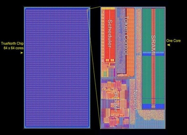
FIGURE 1. IBM’s TrueNorth Chip.
Editor’s Note: This article originally appeared in the October 2018 issue of Solid State Technology.