Tag Archives: letter-ap-tech

Researchers from the University of Texas at Austin and Northwestern University have demonstrated a new method to improve the reliability and performance of transistors and circuits based on carbon nanotubes (CNT), a semiconductor material that has long been considered by scientists as one of the most promising successors to silicon for smaller, faster and cheaper electronic devices. The result appears in a new paper published in the journal Applied Physics Letters, from AIP Publishing.

These are optical images of individual SWCNT field-effect transistors. Credit: S. Jang and A. Dodabalapur/University of Texas at Austin

These are optical images of individual SWCNT field-effect transistors.
Credit: S. Jang and A. Dodabalapur/University of Texas at Austin

In the paper, researchers examined the effect of a fluoropolymer coating called PVDF-TrFE on single-walled carbon nanotube (SWCNT) transistors and ring oscillator circuits, and demonstrated that these coatings can substantially improve the performance of single-walled carbon nanotube devices. PVDF-TrFE is also known by its long chemical name polyvinyledenedifluoride-tetrafluoroethylene.

“We attribute the improvements to the polar nature of PVDF-TrFE that mitigates the negative effect of impurities and defects on the performance of semiconductor single-walled carbon nanotubes,” said Ananth Dodabalapur, a professor in the Cockrell School of Engineering at UT Austin who led the research. “The use of [PVDF-TrFE] capping layers will be greatly beneficial to the adoption of single-walled carbon nanotube circuits in printed electronics and flexible display applications.

The work was done in collaboration between Dodabalapur’s group at UT Austin and Mark Hersam’s group at Northwestern University as part of a Multi-University Research Initiative (MURI) supported by the Office of Naval Research.

A potential successor to silicon chips

Single-walled carbon nanotubes (SWCNT) are just about the thinnest tubes that can be wrought from nature. They are cylinders formed by rolling up a material known as graphene, which is a flat, single-atom-thick layer of carbon graphite. Most single-walled carbon nanotubes typically have a diameter close to 1 nanometer and can be twisted, flattened and bent into small circles or around sharp bends without breaking. These ultra-thin carbon filaments have high mobility, high transparency and electric conductivity, making them ideal for performing electronic tasks and making flexible electronic devices like thin film transistors, the on-off switches at the heart of digital electronic systems.

“Single-walled carbon nanotube field-effect transistors (FETs) have characteristics similar to polycrystalline silicon FETs, a thin film silicon transistor currently used to drive the pixels in organic light-emitting (OLED) displays,” said Mark Hersam, Dodabalapur’s coworker and a professor in the McCormick School of Engineering and Applied Science at Northwestern University. “But single-walled carbon nanotubes are more advantageous than polycrystalline silicon in that they are solution-processable or printable, which potentially could lower manufacturing costs.”

The mechanical flexibility of single-walled carbon nanotubes also should allow them to be incorporated into emerging applications such as flexible electronics and wearable electronics, he said.

For years, scientists have been experimenting with carbon nanotube devices as a successor to silicon devices, as silicon could soon meet its physical limit in delivering increasingly smaller, faster and cheaper electronic devices. Although circuits made with single-walled carbon nanotube are expected to be more energy-efficient than silicon ones in future, their drawbacks in field-effect transistors, such as high power dissipation and less stability, currently limit their applications in printed electronics, according to Dodabalapur.

A new technique to improve the performance of SWCNTs devices

To overcome the drawbacks of single-walled carbon nanotube field-effect transistors and improve their performance, the researchers deposited PVDF-TrFE on the top of self-fabricated single-walled carbon nanotube transistors by inkjet printing, a low-cost, solution based deposition process with good spatial resolution. The fluoropolymer coated film was then annealed or heated in air at 140 degrees Celsius for three minutes. Later, researchers observed the differences of device characteristics.

“We found substantial performance improvements with the fluoropolymer coated single-walled carbon nanotube both in device level and circuit level,” Dodabalapur noted.

On the device level, significant decreases occur in key parameters such as off-current magnitude, degree of hysteresis, variation in threshold voltage and bias stress degradation, which, Dodabalapur said, means a type of more energy-efficient, stable and uniform transistors with longer life time.

On the circuit level, since a transistor is the most basic component in digital circuits, the improved uniformity in device characteristics, plus the beneficial effects from individual transistors eventually result in improved performance of a five-stage complementary ring oscillator circuit, one of the simplest digital circuits.

“The oscillation frequency and amplitude [of the single-walled carbon nanotube ring oscillator circuit] has increased by 42 percent and 250 percent respectively,” said Dodabalapur. The parameters indicate a faster and better performing circuit with possibly reduced power consumption.

Dodabalapur and his coworkers attributed the improvements to the polar nature of PVDF-TrFE.

“Before single-walled carbon nanotube field-effect transistors were fabricated by inkjet printing, they were dispersed in an organic solvent to make a printable ink. After the fabrication process, there could be residual chemicals left [on the device], causing background impurity concentration,” Dodabalapur explained. “These impurities can act as charged defects that trap charge carriers in semiconductors and reduce carriers’ mobility, which eventually could deteriorate the performance of transistors.”

PVDF-TrFE is a polar molecule whose negative and positive charges are separated on different ends of the molecule, Dodabalapur said. The two charged ends form an electric bond, or dipole, in between. After the annealing process, the dipoles in PVDF-TrFE molecules uniformly adopt a stable orientation that tends to cancel the effects of the charged impurities in single-walled carbon nanotube field-effect transistors, which facilitated carrier flow in the semiconductor and improved device performance.

To confirm their hypothesis, Dodabalapur and his coworkers performed experiments comparing the effects of polar and non-polar vapors on single-walled carbon nanotube field-effect transistors. The results support their assumption.

The next step, Dodabalapur said, is to implement more complex circuits with single-walled carbon nanotube field-effect transistors.

The National Science Foundation (NSF) and Semiconductor Research Corporation (SRC) today announced nine research awards to 10 universities totaling nearly $4 million under a joint program focused on Secure, Trustworthy, Assured and Resilient Semiconductors and Systems (STARSS).

The awards support research at the circuit, architecture and system levels on new strategies, methods and tools to decrease the likelihood of unintended behavior or access; increase resistance and resilience to tampering; and improve the ability to provide authentication throughout the supply chain and in the field.

“The processes and tools used to design and manufacture semiconductors ensure that the resulting product does what it is supposed to do. However, a key question that must also be addressed is whether the product does anything else, such as behaving in ways that are unintended or malicious,” said Keith Marzullo, division director of NSF’s Computer and Network Systems Division, which leads the NSF/SRC partnership on STARSS. “Through this partnership with SRC, we are pleased to focus on hardware and systems security research addressing this challenge and to provide a unique opportunity to facilitate the transition of this research into practical use.”

NSF’s involvement in STARSS is part of its Secure and Trustworthy Cyberspace (SaTC) portfolio, which in August announced nearly $75 million in cybersecurity awards.

The STARRS program expands SRC’s Trustworthy and Secure Semiconductors and Systems (T3S) program, engaging 10 universities across the U.S. Initial T3S industry participants are Freescale, Intel Corporation and Mentor Graphics. NSF is the first federal partner.

“The goal of SRC’s T3S initiative is to develop cost-effective strategies and tools for the design and manufacture of chips and systems that are reliable, trustworthy and secure,” said Celia Merzbacher, SRC Vice President for Innovative Partnerships. “This includes designing for security and assurance at the outset so as to build in resistance and resilience to attack or tampering. The research enabled by the STARSS program with NSF is a cornerstone of this overall effort.”

SRC is a university-research consortium for semiconductors and related technologies.

A number of trends are motivating industry and government to support research in hardware and system security. The design and manufacture of semiconductor circuits and systems requires many steps and involves the work of hundreds of engineers — typically distributed across multiple locations and organizations worldwide. Moreover, a typical microprocessor is likely to include dozens of design modules from various sources. Designers at each level need assurance that the components being incorporated can be trusted in order for the final system to be trustworthy.

Today, the design and manufacture of semiconductor circuits and systems includes extensive verification and testing to ensure the final product does what it is intended to do. Similar approaches are needed to provide assurance that the product is authentic and does not allow unwanted functionality, access or control. This includes strategies, tools and methods at all stages, from architecture through manufacture  and throughout the lifecycle of the product.

The first round of awards made through the STARSS program will support nine research projects with diverse areas of focus. They are:

·      “Combating integrated circuit counterfeiting using secure chip odometers” – Carnegie Mellon University researchers will design and implement secure chip odometers to provide integrated circuits (ICs) with both a secure gauge of use/age and an authentication of provenance to detect counterfeit ICs;

·      “Intellectual Property (IP) Trust-A comprehensive framework for IP integrity validation”- Case Western Reserve University and University of Florida researchers will develop a comprehensive and scalable framework for IP trust analysis and verification by evaluating IPs of diverse types and forms and develop threat models, taxonomy and instances of IP trust/integrity issues.

·      “Design of low-cost, memory-based security primitives and techniques for high-volume products” – University of Connecticut researchers will develop metrics and algorithms to make static RAM physical “unclonable” functions that are substantially more reliable at extreme operating conditions and aging, and extend this to dynamic RAM and Flash;

·      “Trojan detection and diagnosis in mixed-signal systems using on-the-fly learned, pre-computed and side channel tests” – Georgia Institute of Technology researchers will leverage knowledge of state of the art mixed-signal/analog/radio frequency for detection of Trojans in generic mixed-signal systems;

·      “Metric and CAD for differential power analysis (DPA) resistance” – Iowa State University researchers will investigate statistical metrics and design techniques to measure and defend against DPA attacks;

·      “Design of secure and anti-counterfeit integrated circuits” – University of Minnesota researchers will develop hierarchical approaches for authentication and obfuscation of chips;

·      “Hardware authentication through high-capacity, physical unclonable functions (PUF)-based secret key generation and lattice coding” – University of Texas at Austin researchers will develop strong machine-learning resistant PUFs, capable of producing high-entropy outputs, and a new lattice-based stability algorithm for high-capacity secret key generation; and

·      “Fault-attack awareness using microprocessor enhancements” – Virginia Institute of Technology and State University researchers will develop a collection of hardware techniques for microprocessor architectures to detect fault injection attacks, and to mitigate fault analysis through an appropriate response in software.

·      “Invariant carrying machine for hardware assurance” – Northwestern University researchers will develop techniques for improving the reliability and trustworthiness of hardware systems via an Invariant-Carrying Machine approach.

Silicon has few serious competitors as the material of choice in the electronics industry. Yet transistors, the switchable valves that control the flow of electrons in a circuit, cannot simply keep shrinking to meet the needs of powerful, compact devices; physical limitations like energy consumption and heat dissipation are too significant.

Now, using a quantum material called a correlated oxide, Harvard researchers have achieved a reversible change in electrical resistance of eight orders of magnitude, a result the researchers are calling “colossal.” In short, they have engineered this material to perform comparably with the best silicon switches.

The finding arose in what may seem an unlikely spot: a laboratory usually devoted to studying fuel cells—the kind that run on methane or hydrogen—led by Shriram Ramanathan, Associate Professor of Materials Science at the Harvard School of Engineering and Applied Sciences (SEAS). The researchers’ familiarity with thin films and ionic transport enabled them to exploit chemistry, rather than temperature, to achieve the dramatic result.

Because the correlated oxides can function equally well at room temperature or a few hundred degrees above it, it would be easy to integrate them into existing electronic devices and fabrication methods. The discovery, published in Nature Communications, therefore firmly establishes correlated oxides as promising semiconductors for future three-dimensional integrated circuits as well as for adaptive, tunable photonic devices.

Challenging silicon

Although electronics manufacturers continue to pack greater speed and functionality into smaller packages, the performance of silicon-based components will soon hit a wall.

“Traditional silicon transistors have fundamental scaling limitations,” says Ramanathan. “If you shrink them beyond a certain minimum feature size, they don’t quite behave as they should.”

Yet silicon transistors are hard to beat, with an on/off ratio of at least 104 required for practical use. “It’s a pretty high bar to cross,” Ramanathan explains, adding that until now, experiments using correlated oxides have produced changes of only about a factor of 10, or 100 at most, near room temperature. But Ramanathan and his team have crafted a new transistor, made primarily of an oxide called samarium nickelate, that in practical operation achieves an on/off ratio of greater than 105—that is, comparable to state-of-the-art silicon transistors.

In future work the researchers will investigate the device’s switching dynamics and power dissipation; meanwhile, this advance represents an important proof of concept.

“Our orbital transistor could really push the frontiers of this field and say, you know what? This is a material that can challenge silicon,” Ramanathan says.

Solid-state chemical doping

Materials scientists have been studying the family of correlated oxides for years, but the field is still in its infancy, with most research aimed at establishing the materials’ basic physical properties.

“We have just discovered how to dope these materials, which is a foundational step in the use of any semiconductor,” says Ramanathan.

Doping is the process of introducing different atoms into the crystal structure of a material, and it affects how easily electrons can move through it—that is, to what extent it resists or conducts electricity. Doping typically effects this change by increasing the number of available electrons, but this study was different. The Harvard team manipulated the band gap, the energy barrier to electron flow.

“By a certain choice of dopants—in this case, hydrogen or lithium—we can widen or narrow the band gap in this material, deterministically moving electrons in and out of their orbitals,” Ramanathan says. That’s a fundamentally different approach than is used in other semiconductors. The traditional method changes the energy level to meet the target; the new method moves the target itself.

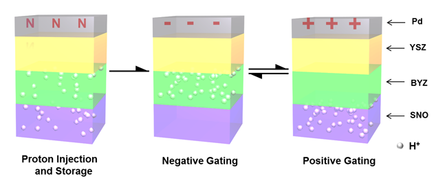
In this orbital transistor, protons and electrons move in or out of the samarium nickelate when an electric field is applied, regardless of temperature, so the device can be operated in the same conditions as conventional electronics. It is solid-state, meaning it involves no liquids, gases, or moving mechanical parts. And, in the absence of power, the material remembers its present state—an important feature for energy efficiency.

“That’s the beauty of this work,” says Ramanathan. “It’s an exotic effect, but in principle it’s highly compatible with traditional electronic devices.”

Quantum materials

Unlike silicon, samarium nickelate and other correlated oxides are quantum materials, meaning that quantum-mechanical interactions have a dominant influence over the material properties—and not just at small scales.

“If you have two electrons in adjacent orbitals, and the orbitals are not completely filled, in a traditional material the electrons can move from one orbital to another. But in the correlated oxides, the electrons repulse each other so much that they cannot move,” Ramanathan explains. “The occupancy of the orbitals and the ability of electrons to move in the crystal are very closely tied together—or ‘correlated.’ Fundamentally, that’s what dictates whether the material behaves as an insulator or a metal.”

Ramanathan and others at SEAS have successfully manipulated the metal-insulator transition in vanadium oxide, too. In 2012, they demonstrated a tunable device that can absorb 99.75% of infrared light, appearing black to infrared cameras.

Similarly, samarium nickelate is likely to catch the attention of applied physicists developing photonic and optoelectronic devices.

“Opening and closing the band gap means you can now manipulate the ways in which electromagnetic radiation interacts with your material,” says Jian Shi, lead author of the paper in Nature Communications. He completed the research as a postdoctoral fellow in Ramanathan’s lab at Harvard SEAS and joined the faculty of Rensselaer Polytechnic Institute this fall. “Just by applying an electric field, you’re dynamically controlling how light interacts with this material.”

Further ahead, researchers at the Center for Integrated Quantum Materials, established at Harvard in 2013 through a grant from the National Science Foundation, aim to develop an entirely new class of quantum electronic devices and systems that will transform signal processing and computation.

Ramanathan compares the current state of quantum materials research to the 1950s, when transistors were newly invented and physicists were still making sense of them. “We are basically in that era for these new quantum materials,” he says. “This is an exciting time to think about establishing the basic, fundamental properties. In the coming decade or so, this could really mature into a very exciting device platform.”

You Zhou, a graduate student at Harvard SEAS, was co-lead author of the paper in Nature Communications. The research was supported by grants from the National Science Foundation (NSF) (CCF-0926148) and the National Academy of Sciences, as well as an NSF Faculty Early Career Development (CAREER) Award to Prof. Ramanathan (DMR-0952794).

Samsung Electronics announced today that it has begun mass producing its six gigabit (Gb) low-power double data rate 3 (LPDDR3) mobile DRAM, based on advanced 20 nanometer (nm) process technology. The new mobile memory chip will enable longer battery run-time and faster application loading on large screen mobile devices with higher resolution.

“Our new 20nm 6Gb LPDDR3 DRAM provides the most advanced mobile memory solution for the rapidly expanding high-performance mobile DRAM market,” said Jeeho Baek, vice president, memory marketing, Samsung Electronics. “We are working closely with our global customers to offer next-generation mobile memory solutions that can be applied to a more extensive range of markets ranging from the premium to standard segments.”

Samsung’s new 6Gb LPDDR3 has a per-pin data transfer rate of up to 2,133 megabits per second (Mbps). A 3GB (gigabyte) LPDDR3 package, which consists of four 6Gb LPDDR3 chips, can be easily created for use in a wide range of mobile devices. Also, the package greatly strengthens our product portfolio for premium mobile applications.

The new 3GB package is more than 20 percent smaller and consumes about 10 percent less energy than the currently available 3GB package with 6Gb LPDDR3 chips fabricated using Samsung’s previously lowest process technology. This results in a mobile memory that is ultra-small, incredibly thin, lightning fast and significantly more power-efficient.

Utilizing Samsung’s new 20nm process also brings more than a 30 percent productivity gain, compared to the previous process. Samsung first applied 20nm technology on 4Gb DDR3 for PCs in March, for the first time in the industry, and has now expanded its use to include the company’s mobile DRAM.

In the future, Samsung will continue to introduce more advanced 20nm mobile DRAM products to further strengthen its product line-up and maintain its leadership in the high-density mobile DRAM market, as the market expands with more feature-laden flagship smartphones, high-end tablets and wearable devices.

You can’t fix what you can’t find. You can’t control what you can’t measure. 

BY DAVID W. PRICE and DOUGLAS G. SUTHERLAND

This is the first in a series of 10 installments which will discuss fundamental truths about process control—inspection and metrology—for the semiconductor industry. By fundamental, we imply the following:

  • Unassailable: They are self-evident, can be proven from first principles, or are supported by the dominant behavior at fabs worldwide
  • Unchanging: these concepts are equally true today for 28nm as they were 15 years ago for 0.25μm, and are expected to hold true in the future
  • Universal: They are not unique to a specific segment of process control; rather they apply to process control as a group, as well as to each individual component of process control within the fab

Each article in this series will introduce one of the 10 fundamental truths and discuss interesting applications of these truths to semiconductor IC fabs. Given the increasing complexity of advanced devices and process integration, process control is growing in importance. By understanding the fundamental nature of process control, fabs can better implement strategies to identify critical defects, find excursions, and reduce sources of variation.

The first fundamental truth of process control for the semiconductor IC industry is:

You can’t fix what you can’t find. You can’t control what you can’t measure.

While it’s true that inspection and metrology systems are not used to make IC devices—they do not add or remove materials or create patterns—they are critical for making high-yielding, reliable devices. By finding defects and measuring critical parameters, inspection and metrology systems monitor the hundreds of steps required to manufacture a device, ensuring the processes meet strict manufacturing specifications and helping fab engineers identify and troubleshoot process issues when there is an excursion. Without inspection and metrology, it would be near impossible for fabs to pinpoint process issues that affect yield. However, it’s not enough to simply “find” and “measure” — a fab’s process control strategy needs to be capable and cost-effective.

Capable inspection and metrology strategies find and measure the defects and parameters that affect device yield. Cost-effective inspection and metrology is performed at the lowest total cost to the factory, where total cost is the sum of the cost of lost yield plus the cost of process control.

First, make it capable

If you can’t find it, you can’t fix it. At the heart of this truth is the understanding that, above all else, a fab’s inspection and metrology strategy must be capable. It must highlight the problems that are limiting baseline yield. It must also provide actionable information that can enable fabs to quickly find and fix excursions (FIGURE 1).

We emphasize this need for capability first because we have observed that some fabs are too quick tosacrifice capability for cost reductions. No strategy is cost-effective if it doesn’t accomplish its fundamental objective.

Below are specific questions that can help fab management evaluate the capability of its process control strategy:

  • Are you finding all sources of your defect-limited yield? Are you finding these in-line or at end-of-line?
  • Does your defect Pareto have sufficient resolution of the top yield-limiters in each module to direct the most appropriate use of factory engineering resources?
  • Have you fully characterized all of the important measurements and defect types (size range, kill ratio, root cause, solution)?
  • Do you understand the most probable incursion scenarios? What is the smallest excursion that you absolutely must detect at this step? How many lots are you willing to have exposed to this excursion before it is detected?
  • Are you inspecting and measuring at all the right steps? Can you quickly isolate the point of formation for excursions? Can you quickly disposition potentially affected lots?
  • Does a particular defect signature become confused by defects added at subsequent process steps? Or do you need separate inspections at each step in order to partition the problem? 
  • Do you have overlapping inspections to guard against the high-frequency, high-impact excursions?
  • What is the alpha risk and beta risk for each inspection or measurement? How are these related to the capture rate, accuracy, precision, matching and more?

Process control Fig 1b Process control fig 1a


FIGURE 1. You can’t fix what you can’t find. And you can’t control what you can’t measure. Left: P-MOS SiGe critical dimension measurement. Right: Fin patterning particle leading to a Fin Spire defect at post dummy gate etch. Source: KLA-Tencor

Then, make it cost-effective

Once a capable strategy is in place, then a fab can start the process of making it cost-effective. The best known method for optimizing total cost is usually adjusting the overall lot sampling rate. This is generally preferred because the capability remains constant.

In some cases, it may be possible to migrate to a less sensitive inspection (lower cost of ownership tool or larger pixel size); however, this is a dangerous path because it re-introduces uncertainty (alpha/beta risk) that reduces a fab’s process control capability. This concept will be discussed in more detail in our next article on sampling strategies.

Finally, it is worth pointing out that it is not enough to implement a capable strategy. The fab must ensure that what was once a capable strategy, stays a capable strategy. A fab cannot measure with a broken inspection tool or trust a poorly maintained inspection tool. Therefore, most fabs have programs in place to maintain and monitor the ongoing performance of their inspection and metrology tools.

By optimizing process control strategy to be capable and cost-effective, fabs ultimately find what needs to be fixed and measure what should be controlled—driving higher yield and better profitability.

Ziptronix Inc. today announced that its Direct Bond Interconnect (DBI) hybrid bonding has been implemented by Fermi National Accelerator Laboratory (Fermilab) to improve the performance of high-end 3D sensor arrays, which are used for particle detection in large-scale particle physics and x-ray imaging experiments. This is an example of three-layer DBI hybrid bonding in a 3D imaging chip, using DBI wafer-to-wafer and die-to-wafer processes.

The demonstrator, a vertically integrated x-ray photon imaging chip (VIPIC) detector, was developed by a collaboration of scientists and engineers from Fermilab, Brookhaven National Laboratory and AGH University from Poland. DBI hybrid bonding technology enables versatile new designs for pixelated radiation detectors. Fermilab and Brookhaven are national laboratories funded by the U.S. Department of Energy.

“Implementing DBI hybrid bonding enables us to design sophisticated combinations of sensors and readout electronics,” said Ron Lipton, Staff Scientist, Fermilab. “By enabling vertical signals through stacked sensor, readout and processing layers, we can design large-scale arrays that are side-edge buttable with high fill factor.”

The process flow for manufacturing the VIPIC involves using wafer-to-wafer DBI hybrid bonding to bond two ASIC wafers containing through silicon vias (TSVs). The bonded wafer pair is thinned to expose the TSVs on one side, then singulated. The singulated die stacks are then bonded to an x-ray sensor wafer using die-to-wafer DBI hybrid bonding. Subsequent thinning of the other side of the bonded wafer pair allows backside connections to the 3-layer assembly.

“This is an advanced three-layer imaging chip manufactured using DBI hybrid bonding,” said Paul Enquist, CTO, Ziptronix. “Electrical data shows that this approach achieves lower noise, higher bandwidth and higher gain due to lower capacitive load when compared with parts stacked using bumping. This increases the sensitivity of the 3D image sensors, making them ideal for use in high-end applications.”

DBI hybrid bonding is a conductor/dielectric bonding technology that includes a variety of metal/oxide/nitride combinations, uses no adhesives and is CMOS foundry compatible. It allows for stronger bonds and finer-pitch interconnect over traditional thermocompression bonding since bonding occurs at both the conductive and dielectric materials, versus just the conductor. Bonding therefore takes place over the entire surface area, eliminating the need for underfill as well as significantly reducing the overall height of the structure.

GLOBALFOUNDRIES, a provider of advanced semiconductor manufacturing technology, today announced the “GLOBALFOUNDRIES Undergraduate Research Scholarship,” a new scholarship recognizing and rewarding aspiring, leadership-oriented engineering students interested in careers in the semiconductor industry.  The GLOBALFOUNDRIES Undergraduate Research Scholarship will fund undergraduate research opportunities (URO) and intern scholars through the Semiconductor Research Corporation’s (SRC) Education Alliance.

Presented at SRC’s annual TECHCON conference in Austin, Texas, the scholarship was created by GLOBALFOUNDRIES in partnership with SRC to recognize and reward science, technology and engineering students who demonstrate promise in their academic and professional efforts. The selected recipients of this scholarship will have the opportunity to interact with GLOBALFOUNDRIES researchers and access the professional resources of SRC and the SRC Education Alliance.

“Building a pipeline of highly skilled talent is essential to our business and to the competitiveness of the entire semiconductor industry,” said Suresh Venkatesan, senior vice president of technology development, GLOBALFOUNDRIES.  “SRC connects companies with the top universities, which results in exciting research and educational opportunities for the best and the brightest students. The GLOBALFOUNDRIES Undergraduate Research Scholarship gives us the opportunity to support science, technology, engineering and mathematics education and help develop the technical leaders who will continue to drive innovation in the semiconductor industry in the future.”

Until recently, SRC focused exclusively on students seeking advanced degrees, providing fellowships for them to do university research that had practical applications for corporate members of its unique consortium. The URO is SRC’s innovative program providing undergraduates with valuable research experience and mentoring. The goal of the URO is to empower bright, well-educated, and experienced scientists and engineers for which U.S. high-tech companies are seeking.

“Recognizing the critical importance of a strong pipeline of new talent for the semiconductor industry, the SRC Education Alliance through the URO Program provides financial assistance to undergraduates, allowing students and universities to recognize the connections between the materials they are learning in the classroom and the technological innovations that transform the world,” said SRC President Larry Sumney. “We are thrilled to collaborate with GLOBALFOUNDRIES as we continue to develop our URO program.”

Rising sophomores, juniors and seniors in an accredited undergraduate program majoring in the field of engineering are encouraged to apply.  Additional information about the scholarship can be obtained by visiting: www.src.org/program/srcea/uro/globalfoundries.

Every year, TECHCON brings together the brightest minds in microelectronics research to exchange news about the progress of new materials and processes created by SRC’s network of more than 100 of the top engineering universities. Students and industry leaders discuss basic research that is intended to accelerate advancements for both private and public entities.

Graphene is a semiconductor when prepared as an ultra-narrow ribbon – although the material is actually a conductive material. Researchers from Empa and the Max Planck Institute for Polymer Research have now developed a new method to selectively dope graphene molecules with nitrogen atoms. By seamlessly stringing together doped and undoped graphene pieces, they were able to form ”heterojunctions” in the nanoribbons, thereby fulfilling a basic requirement for electronic current to flow in only one direction when voltage is applied – the first step towards a graphene transistor. Furthermore, the team has successfully managed to remove graphene nanoribbons from the gold substrate on which they were grown and to transfer them onto a non-conductive material.

Graphene possesses many outstanding properties: it conducts heat and electricity, it is transparent, harder than diamond and extremely strong. But in order to use it to construct electronic switches, a material must not only be an outstanding conductor, it should also be switchable between ”on” and ”off” states. This requires the presence of a so-called bandgap, which enables semiconductors to be in an insulating state. The problem, however, is that the bandgap in graphene is extremely small. Empa researchers from the ”nanotech@surfaces” laboratory thus developed a method some time ago to synthesise a form of graphene with larger bandgaps by allowing ultra-narrow graphene nanoribbons to ”grow” via molecular self-assembly.

Graphene nanoribbons made of differently doped segments

The researchers, led by Roman Fasel, have now achieved a new milestone by allowing graphene nanoribbons consisting of differently doped subsegments to grow. Instead of always using the same ”pure” carbon molecules, they used additionally doped molecules – molecules provided with ”foreign atoms” in precisely defined positions, in this case nitrogen. By stringing together ”normal” segments with nitrogen-doped segments on a gold (Au (111)) surface, so-called heterojunctions are created between the individual segments. The researchers have shown that these display similar properties to those of a classic p-n-junction, i.e. a junction featuring both positive and negative charges across different regions of the semiconductor crystal, thereby creating the basic structure allowing the development of many components used in the semiconductor industry. A p-n junction causes current to flow in only one direction. Because of the sharp transition at the heterojunction interface, the new structure also allows electron/hole pairs to be efficiently separated when an external voltage is applied, as demonstrated theoretically by theorists at Empa and collaborators at Rensselaer Polytechnic Institute The latter has a direct impact on the power yield of solar cells. The researchers describe the corresponding heterojunctions in segmented graphene nanoribbons in the recently published issue of “Nature Nanotechnology.”

Transferring graphene nanoribbons onto other substrates

In addition, the scientists have solved another key issue for the integration of graphene nanotechnology into conventional semiconductor industry: how to transfer the ultra-narrow graphene ribbons onto another surface? As long as the graphene nanoribbons remain on a metal substrate (such as gold used here) they cannot be used as electronic switches. Gold conducts and thus creates a short-circuit that “sabotages” the appealing semiconducting properties of the graphene ribbon. Fasel’s team and colleagues at the Max-Planck-Institute for Polymer Research in Mainz have succeeded in showing that graphene nanoribbons can be transferred efficiently and intact using a relatively simple etching and cleaning process onto (virtually) any substrate, for example onto sapphire, calcium fluoride or silicon oxide.

Graphene is thus increasingly emerging as an interesting semiconductor material and a welcome addition to the omnipresent silicon. The semiconducting graphene nanoribbons are particularly attractive as they allow smaller and thus more energy efficient and faster electronic components than silicon. However, the generalized use of graphene nanoribbons in the electronics sector is not anticipated in the near future, due in part to scaling issues and in part to the difficulty of replacing well-established conventional silicon-based electronics. Fasel estimates that it may still take about 10 to 15 years before the first electronic switch made of graphene nanoribbons can be used in a product.

Graphene nanoribbons for photovoltaic components

Photovoltaic components could also one day be based on graphene. In a second paper published in Nature Communications, Pascal Ruffieux – also from the Empa “nanotech@surfaces” laboratory – and his colleagues describe a possible use of graphene strips, for instance in solar cells. Ruffieux and his team have noticed that particularly narrow graphene nanoribbons absorb visible light exceptionally well and are therefore highly suitable for use as the absorber layer in organic solar cells. Compared to “normal” graphene, which absorbs light equally at all wavelengths, the light absorption in graphene nanoribbons can be increased enormously in a controlled way, whereby researchers “set” the width of the graphene nanoribbons with atomic precision.

Cree, Inc. has announced that its C2M, 1200V, 80mOhm SiC MOSFETs have been selected by Sanix Corporation, Japan, to be designed into their new 9.9kW three-phase solar inverters for use in the construction of commercial photovoltaic systems in the fast-growing Japanese solar energy market.

“Through this partnership with Cree and their SiC technology, Sanix is able to capture more market share in the competitive Japan solar market,” said Hiroshi Soga, general manager, Sanix Incorporated. “Cree’s silicon carbide MOSFETs were critical for Sanix to meet our efficiency and thermal design targets. SiC switches reduced losses in our inverter electronics by more than 30 percent versus the silicon super-junction MOSFETs we were considering. In addition to providing a large efficiency gain, Cree’s latest generation C2M SiC MOSFETs were priced competitively, making it possible to replace lower voltage, less rugged, and less efficient silicon MOSFETs.”

Utilized in the primary power conversion stage of the solar inverter, Cree’s 1200V C2M0080120D MOSFETs feature faster switching characteristics and up to one-third the switching losses of comparably-rated 900V silicon super-junction MOSFETs. By significantly reducing switching losses, Cree’s SiC MOSFETs enable lower total system energy losses, higher frequency switching, and cooler operating temperatures. These benefits improve conversion efficiency and reduce the system’s size, weight, complexity, and thermal management requirements. At the system level, performance is improved, cost is decreased, and lifetime of the inverter is extended.

“Cree is extremely pleased that Sanix has chosen to specify our C2M, 1200V SiC MOSFET technology in its new 9.9kW solar inverters. Cree SiC power devices can provide significant advantages with regard to PV inverter efficiency, reliability, and cost, and will provide Sanix with a critical competitive advantage as they continue to expand their share of the Japanese solar market,” said Cengiz Balkas, general manager and vice president, Cree Power and RF.

Demonstrated to achieve up to three times the power density of typical silicon technology, Cree’s C2M family of SiC MOSFETs are available in 1200V and 1700V, ranging from 1Ω to 25 mΩ. C2M MOSFETs have been designed into a range of industrial power applications since their March 2013 market introduction and continue to experience increasing demand. Cree is currently delivering production volumes of SiC MOSFETs to Sanix and other PV inverter manufacturers, as well as to makers of industrial power supplies, auxiliary power converters, battery chargers, and motor drives.

Move over, graphene. An atomically thin, two-dimensional, ultrasensitive semiconductor material for biosensing developed by researchers at UC Santa Barbara promises to push the boundaries of biosensing technology in many fields, from health care to environmental protection to forensic industries.

Based on molybdenum disulfide or molybdenite (MoS2), the biosensor material — used commonly as a dry lubricant — surpasses graphene’s already high sensitivity, offers better scalability and lends itself to high-volume manufacturing. Results of the researchers’ study have been published in ACS Nano.

Concept art of a molybdenum disulfide field-effect transistor based biosensor demonstrated by UCSB researchers with ability to detect ultra-low (femtomolar) concentrations with high sensitivity that is 74-fold higher than that of graphene FET biosensors. - Photo Credit: Peter Allen

Concept art of a molybdenum disulfide field-effect transistor based biosensor demonstrated by UCSB researchers with ability to detect ultra-low (femtomolar) concentrations with high sensitivity that is 74-fold higher than that of graphene FET biosensors. – Photo Credit: Peter Allen

“This invention has established the foundation for a new generation of ultrasensitive and low-cost biosensors that can eventually allow single-molecule detection — the holy grail of diagnostics and bioengineering research,” said Samir Mitragotri, co-author and professor of chemical engineering and director of the Center for Bioengineering at UCSB. “Detection and diagnostics are a key area of bioengineering research at UCSB and this study represents an excellent example of UCSB’s multifaceted competencies in this exciting field.”

The key, according to UCSB professor of electrical and computer engineering Kaustav Banerjee, who led this research, is MoS2’s band gap, the characteristic of a material that determines its electrical conductivity.

Semiconductor materials have a small but nonzero band gap and can be switched between conductive and insulated states controllably. The larger the band gap, the better its ability to switch states and to insulate leakage current in an insulated state. MoS2’s wide band gap allows current to travel but also prevents leakage and results in more sensitive and accurate readings.

The limitations of graphene

While graphene has attracted wide interest as a biosensor due to its two-dimensional nature that allows excellent electrostatic control of the transistor channel by the gate, and high surface-to-volume ratio, the sensitivity of a graphene field-effect transistor (FET) biosensor is fundamentally restricted by the zero band gap of graphene that results in increased leakage current, leading to reduced sensitivity, explained Banerjee, who is also the director of the Nanoelectronics Research Lab at UCSB.

Graphene has been used, among other things, to design FETs — devices that regulate the flow of electrons through a channel via a vertical electric field directed into the channel by a terminal called a “gate.” In digital electronics, these transistors control the flow of electricity throughout an integrated circuit and allow for amplification and switching.

In the realm of biosensing, the physical gate is removed, and the current in the channel is modulated by the binding between embedded receptor molecules and the charged target biomolecules to which they are exposed. Graphene has received wide interest in the biosensing field and has been used to line the channel and act as a sensing element whose surface potential (or conductivity) can be modulated by the interaction (known as conjugation) between the receptor and target molecules that results in net accumulation of charges over the gate region.

However, said the research team, despite graphene’s excellent characteristics, its performance is limited by its zero band gap. Electrons travel freely across a graphene FET — hence, it cannot be “switched off” — which in this case results in current leakages and higher potential for inaccuracies.

Much research in the graphene community has been devoted to compensating for this deficiency, either by patterning graphene to make nanoribbons or by introducing defects in the graphene layer — or using bilayer graphene stacked in a certain pattern that allows band gap opening upon application of a vertical electric field — for better control and detection of current.

Enter MoS2, a material already making waves in the semiconductor world for the similarities it shares with graphene, including its atomically thin hexagonal structure, and planar nature, as well as what it can do that graphene can’t: act like a semiconductor.

“Monolayer or few-layer MoS2 have a key advantage over graphene for designing an FET biosensor: They have a relatively large and uniform band gap (1.2-1.8 eV, depending on the number of layers) that significantly reduces the leakage current and increases the abruptness of the turn-on behavior of the FETs, thereby increasing the sensitivity of the biosensor,” said Banerjee.

‘The best of everything’

Additionally, according to Deblina Sarkar, a PhD student in Banerjee’s lab and the lead author of the article, two-dimensional MoS2 is relatively simple to manufacture.

“While one-dimensional materials such as carbon nanotubes and nanowires also allow excellent electrostatics and at the same time possess band gap, they are not suitable for low-cost mass production due to their process complexities,” she said. “Moreover, the channel length of MoS2 FET biosensor can be scaled down to the dimensions similar to those of small biomolecules such as DNA or small proteins, still maintaining good electrostatics, which can lead to high sensitivity even for detection of single quanta of these biomolecular species,” she added.

“In fact, atomically thin MoS2 provides the best of everything: great electrostatics due to their ultra-thin body, scalability (due to large band gap), as well as patternability due to their planar nature that is essential for high-volume manufacturing,” said Banerjee.

The MoS2 biosensors demonstrated by the UCSB team have already provided ultrasensitive and specific protein sensing with a sensitivity of 196 even at 100 femtomolar (a billionth of a millionth of a mole) concentrations. This protein concentration is similar to one drop of milk dissolved in a hundred tons of water. An MoS2-based pH sensor achieving sensitivity as high as 713 for a pH change by one unit along with efficient operation over a wide pH range (3-9) is also demonstrated in the same work.

“This transformative technology enables highly specific, low-power, high-throughput physiological sensing that can be multiplexed to detect a number of significant, disease-specific factors in real time,” commented Scott Hammond, executive director of UCSB’s Translational Medicine Research Laboratories.

Biosensors based on conventional FETs have been gaining momentum as a viable technology for the medical, forensic and security industries since they are cost-effective compared to optical detection procedures. Such biosensors allow for scalability and label-free detection of biomolecules — removing the step and expense of labeling target molecules with florescent dye. “In essence,” continued Hammond, “the promise of true evidence-based, personalized medicine is finally becoming reality.”

“This demonstration is quite remarkable,” said Andras Kis, professor at École Polytechnique Fédérale de Lausanne in Switzerland and a leading scientist in the field of 2D materials and devices.

“At present, the scientific community worldwide is actively seeking practical applications of 2D semiconductor materials such as MoS2 nanosheets. Professor Banerjee and his team have identified a breakthrough application of these nanomaterials and provided new impetus for the development of low-power and low-cost ultrasensitive biosensors,” continued Kis, who is not connected to the project.

Wei Liu and Xuejun Xie from UCSB’s Department of Electrical and Computer Engineering and Aaron Anselmo from the Department of Chemical Engineering also conducted research for this study. Research on this project was supported by the National Science Foundation, the California NanoSystems Institute at UCSB and the Materials Research Laboratory at UCSB, a National Science Foundation MRSEC.