Tag Archives: letter-dd-tech

In a sub-basement deep below the Laboratory for Integrated Science and Engineering at Harvard University, Mikhail Kats gets dressed. Mesh shoe covers, a face mask, a hair net, a pale gray jumpsuit, knee-high fabric boots, vinyl gloves, safety goggles, and a hood with clasps at the collar–these are not to protect him, Kats explains, but to protect the delicate equipment and materials inside the cleanroom.

While earning his Ph.D. in applied physics at the Harvard School of Engineering and Applied Sciences, Kats has spent countless hours in this cutting-edge facility. With his adviser, Federico Capasso, the Robert L. Wallace Professor of Applied Physics and Vinton Hayes Senior Research Fellow in Electrical Engineering, Kats has contributed to some stunning advances.

One is a metamaterial that absorbs 99.75 percent of infrared light–very useful for thermal imaging devices. Another is an ultrathin, flat lens that focuses light without imparting the distortions of conventional lenses. And the team has produced vortex beams, light beams that resemble a corkscrew, that could help communications companies transmit more data over limited bandwidth.

Certainly the most colorful advance to emerge from the Capasso lab, however, is a technique that coats a metallic object with an extremely thin layer of semiconductor, just a few nanometers thick. Although the semiconductor is a steely gray color, the object ends up shining in vibrant hues. That’s because the coating exploits interference effects in the thin films; Kats compares it to the iridescent rainbows that are visible when oil floats on water. Carefully tuned in the laboratory, these coatings can produce a bright, solid pink–or, say, a vivid blue–using the same two metals, applied with only a few atoms’ difference in thickness.

Capasso’s research group announced the finding in 2012, but at that time, they had only demonstrated the coating on relatively smooth, flat surfaces like silicon. This fall, the group published a second paper, in the journal Applied Physics Letters, taking the work much further.

“I cut a piece of paper out of my notebook and deposited gold and germanium on it,” Kats says, “and it worked just the same.”

That finding, deceptively simple given the physics involved, now suggests that the ultrathin coatings could be applied to essentially any rough or flexible material, from wearable fabrics to stretchable electronics.

“This can be viewed as a way of coloring almost any object while using just a tiny amount of material,” Capasso says.

It was not obvious that the same color effects would be visible on rough substrates, because interference effects are usually highly sensitive to the angle of light. And on a sheet of paper, Kats explains, “There are hills and valleys and fibers and little things sticking out–that’s why you can’t see your reflection in it. The light scatters.”

On the other hand, the applied films are so extremely thin that they interact with light almost instantaneously, so looking at the coating straight on or from the side–or, as it turns out, looking at those rough imperfections in the paper–doesn’t make much difference to the color. And the paper remains flexible, as usual.

Demonstrating the technique in the cleanroom at the Center for Nanoscale Systems, a National Science Foundation-supported research facility at Harvard, Kats uses a machine called an electron beam evaporator to apply the gold and germanium coating. He seals the paper sample inside the machine’s chamber, and a pump sucks out the air until the pressure drops to a staggering 10^-6 Torr (a billionth of an atmosphere). A stream of electrons strikes a piece of gold held in a carbon crucible, and the metal vaporizes, traveling upward through the vacuum until it hits the paper. Repeating the process, Kats adds the second layer. A little more or a little less germanium makes the difference between indigo and crimson.

This particular lab technique, Kats points out, is unidirectional, so to the naked eye very subtle differences in the color are visible at different angles, where slightly less of the metal has landed on the sides of the paper’s ridges and valleys. “You can imagine decorative applications where you might want something that has a little bit of this pearlescent look, where you look from different angles and see a different shade,” he notes. “But if we were to go next door and use a reactive sputterer instead of this e-beam evaporator, we could easily get a coating that conforms to the surface, and you wouldn’t see any differences.”

Many different pairings of metal are possible, too. “Germanium’s cheap. Gold is more expensive, of course, but in practice we’re not using much of it,” Kats explains. Capasso’s team has also demonstrated the technique using aluminum.

“This is a way of coloring something with a very thin layer of material, so in principle, if it’s a metal to begin with, you can just use 10 nanometers to color it, and if it’s not, you can deposit a metal that’s 30 nm thick and then another 10nm. That’s a lot thinner than a conventional paint coating that might be between a micron and 10 microns thick.”

In those occasional situations where the weight of the paint matters, this could be very significant. Capasso remembers, for example, that the external fuel tank of NASA’s space shuttle used to be painted white. After the first two missions, engineers stopped painting it and saved 600 pounds of weight.

Because the metal coatings absorb a lot of light, reflecting only a narrow set of wavelengths, Capasso suggests that they could also be incorporated into optoelectronic devices like photodetectors and solar cells.

“The fact that these can be deposited on flexible substrates has implications for flexible and maybe even stretchable optoelectronics that could be part of your clothing or could be rolled up or folded,” Capasso says.

Harvard’s Office of Technology Development continues to pursue commercial opportunities for the new color coating technology and welcomes contact from interested parties.

Kats, who concludes his year-long postdoctoral research position at SEAS this month, will become an assistant professor at the University of Wisconsin, Madison, in January. He credits those many hours spent in Harvard’s state-of-the-art laboratory facilities for much of his success in applied physics.

“You learn so much while you’re doing it,” Kats says. “You can be creative, discover something along the way, apply something new to your research. It’s marvelous that we have students and postdocs down here making things.”

A team of researchers led by North Carolina State University has found that  stacking materials that are only one atom thick can create semiconductor junctions that transfer charge efficiently, regardless of whether the crystalline structure of the materials is mismatched – lowering the manufacturing cost for a wide variety of semiconductor devices such as solar cells, lasers and LEDs.

“This work demonstrates that by stacking multiple two-dimensional (2-D) materials in random ways we can create semiconductor junctions that are as functional as those with perfect alignment” says Dr. Linyou Cao, senior author of a paper on the work and an assistant professor of materials science and engineering at NC State.

“This could make the manufacture of semiconductor devices an order of magnitude less expensive.”

Schematic illustration of monolayer MoS2 and WS2 stacked vertically. Image: Linyou Cao.

Schematic illustration of monolayer MoS2 and WS2 stacked vertically. Image: Linyou Cao.

For most semiconductor electronic or photonic devices to work, they need to have a junction, which is where two semiconductor materials are bound together. For example, in photonic devices like solar cells, lasers and LEDs, the junction is where photons are converted into electrons, or vice versa.

All semiconductor junctions rely on efficient charge transfer between materials, to ensure that current flows smoothly and that a minimum of energy is lost during the transfer. To do that in conventional semiconductor junctions, the crystalline structures of both materials need to match. However, that limits the materials that can be used, because you need to make sure the crystalline structures are compatible. And that limited number of material matches restricts the complexity and range of possible functions for semiconductor junctions.

“But we found that the crystalline structure doesn’t matter if you use atomically thin, 2-D materials,” Cao says. “We used molybdenum sulfide and tungsten sulfide for this experiment, but this is a fundamental discovery that we think applies to any 2-D semiconductor material. That means you can use any combination of two or more semiconductor materials, and you can stack them randomly but still get efficient charge transfer between the materials.”

Currently, creating semiconductor junctions means perfectly matching crystalline structures between materials – which requires expensive equipment, sophisticated processing methods and user expertise. This manufacturing cost is a major reason why semiconductor devices such as solar cells, lasers and LEDs remain very expensive. But stacking 2-D materials doesn’t require the crystalline structures to match.

“It’s as simple as stacking pieces of paper on top of each other – it doesn’t even matter if the edges of the paper line up,” Cao says.

The paper, “Equally Efficient Interlayer Exciton Relaxation and Improved Absorption in Epitaxial and Non-epitaxial MoS2/WS2 Heterostructures,” was published as a “just-accepted” manuscript in Nano Letters Dec. 3.

Lead authors of the paper are Yifei Yu, a Ph.D. student at NC State; Dr. Shi Hu, a former postdoctoral researcher at NC State; and Liqin Su, a Ph.D. student at the University of North Carolina at Charlotte. The paper was co-authored by Lujun Huang, Yi Liu, Zhenghe Jin, and Dr. Ki Wook Kim of NC State; Drs. Alexander Puretzky and David Geohegan of Oak Ridge National Laboratory; and Dr. Yong Zhang of UNC Charlotte. The research was funded by the U.S. Army Research Office under grant number W911NF-13-1-0201 and the National Science Foundation under grant number DMR-1352028.

Holst Centre, imec and their partner Evonik have realized a general-purpose 8-bit microprocessor, manufactured using complementary thin-film transistors (TFTs) processed at temperatures compatible with plastic foil substrates (250°C). The new “hybrid” technology integrates two types of semiconductors—metal-oxide for n-type TFTs (iXsenic, Evonik) and organic molecules for p-type TFTs—in a CMOS microprocessor circuit, operating at unprecedented for TFT technologies speed—clock frequency 2.1kHz. The breakthrough results were published online in Scientific Reports, an open access journal from the publisher of Nature.

Low temperature thin-film electronics are based on organic and metal-oxide semiconductors. They have the potential to be produced in a cost effective way using large-area manufacturing processes on plastic foils. Thin-film electronics are, therefore, attractive alternatives for silicon chips in simple IC applications, such as radio frequency identification (RFID) and near field communication (NFC) tags and sensors for smart food packaging, and in large-area electronic applications, such as flexible displays, sensor arrays and OLED lamps. Holst Centre’s (imec and TNO) research into thin-film electronics aims at developing a robust, foil-compatible, high performance technology platform, which is key to making these new applications become a reality.

The novel 8-bit microprocessor performs at a clock frequency of 2.1 kHz. It consists of two separate chips: a processor core chip and a general-purpose instruction generator (P2ROM). For the processor core chip, a complementary hybrid organic-oxide technology was used (p:n ratio 3:1). The n-type transistors are 250°C solution-processed metal-oxide TFTs with typically high charge carrier mobility (2 cm2/Vs). The p-type transistors are small molecule organic TFTs with mobility of up to 1 cm2/Vs. The complementary logic allows for a more complex and complete standard cell library, including additional buffering in the core and the implementation of a mirror adder in the critical path. These optimizations have resulted in a high maximum clock frequency of 2.1kHz. The general-purpose instruction generator or P2ROM is a one-time programmable ROM memory configured by means of inkjet printing, using a conductive silver ink. The chip is divided into a hybrid complementary part and a unipolar n-TFT part and is capable of operating at frequencies up to 650 Hz, at an operational voltage of Vdd=10V.

Interested companies can join Holst Centre’s R&D program on organic and oxide transistors, exploring and developing new technologies for producing thin-film transistors (TFTs) on plastic foils.

thin film microprocessor

Physicists at the University of Kansas have fabricated an innovative substance from two different atomic sheets that interlock much like Lego toy bricks. The researchers said the new material — made of a layer of graphene and a layer of tungsten disulfide — could be used in solar cells and flexible electronics. Their findings are published today by Nature Communications.

Hsin-Ying Chiu, assistant professor of physics and astronomy, and graduate student Matt Bellus fabricated the new material using “layer-by-layer assembly” as a versatile bottom-up nanofabrication technique. Then, Jiaqi He, a visiting student from China, and Nardeep Kumar, a graduate student who now has moved to Intel Corp., investigated how electrons move between the two layers through ultrafast laser spectroscopy in KU’s Ultrafast Laser Lab, supervised by Hui Zhao, associate professor of physics and astronomy.

 “To build artificial materials with synergistic functionality has been a long journey of discovery,” Chiu said. “A new class of materials, made of the layered materials, has attracted extensive attention ever since the rapid development of graphene technology. One of the most promising aspects of this research is the potential to devise next-generation materials via atomic layer-level control over its electronic structure.”

According to the researchers, the approach is to design synergistic materials by combining two single-atom thick sheets, for example, acting as a photovoltaic cell as well as a light-emitting diode, converting energy between electricity and radiation. However, combining layers of atomically thin material is a thorny task that has flummoxed researchers for years.

“A big challenge of this approach is that, most materials don’t connect together because of their different atomic arrangements at the interface — the arrangement of the atoms cannot follow the two different sets of rules at the same time,” Chiu said. “This is like playing with Legos of different sizes made by different manufacturers. As a consequence, new materials can only be made from materials with very similar atomic arrangements, which often have similar properties, too. Even then, arrangement of atoms at the interface is irregular, which often results in poor qualities.”

Layered materials such as those developed by the KU researchers provide a solution for this problem. Unlike conventional materials formed by atoms that are strongly bound in all directions, the new material features two layers where each atomic sheet is composed of atoms bound strongly with their neighbors — but the two atomic sheets are themselves only weakly linked to each other by the so-called van der Waals force, the same attractive phenomenon between molecules that allows geckos to stick to walls and ceilings.

“There exist about 100 different types of layered crystals — graphite is a well-known example,” Bellus said. “Because of the weak interlayer connection, one can choose any two types of atomic sheets and put one on top of the other without any problem. It’s like playing Legos with a flat bottom. There is no restriction. This approach can potentially product a large number of new materials with combined novel properties and transform the material science.”

Chiu and Bellus created the new carbon and tungsten disulfide material with the aim of developing novel materials for efficient solar cells. The single sheet of carbon atoms, known as graphene, excels at moving electrons around, while a single-layer of tungsten disulfide atoms is good at absorbing sunlight and converting it to electricity. By combining the two, this innovative material can potentially perform both tasks well.

The team used scotch tape to lift a single layer of tungsten disulfide atoms from a crystal and apply it to a silicon substrate. Next, they used the same procedure to remove a single layer of carbon atoms from a graphite crystal. With a microscope, they precisely laid the graphene on top of the tungsten disulfide layer. To remove any glue between the two atomic layers that are unintentionally introduced during the process, the material was heated at about 500 degrees Fahrenheit for a half-hour. This allowed the force between the two layers to squeeze out the glue, resulting in a sample of two atomically thin layers with a clean interface.

Doctoral students He and Kumar tested the new material in KU’s Ultrafast Laser Lab. The researchers used a laser pulse to excite the tungsten disulfide layer.

“We found that nearly 100 percent of the electrons that absorbed the energy from the laser pulse move from tungsten disulfide to graphene within one picosecond, or one-millionth of one-millionth second,” Zhao said. “This proves that the new material indeed combines the good properties of each component layer.”

The research groups led by Chiu and Zhao are trying to apply this Lego approach to other materials. For example, by combining two materials that absorb light of different colors, they can make materials that react to diverse parts of the solar spectrum.

The National Science Foundation funded this work.

University of Utah engineers have developed a polarizing filter that allows in more light, leading the way for mobile device displays that last much longer on a single battery charge and cameras that can shoot in dim light.

Polarizers are indispensable in digital photography and LCD displays, but they block enormous amounts of light, wasting energy and making it more difficult to photograph in low light.

The Utah electrical and computer engineering researchers created the filter by etching a silicon wafer with nanoscale pillars and holes using a focused gallium-ion beam. This new concept in light filtering can perform the same function as a standard polarizer but allows up to nearly 30 percent more light to pass through, says U electrical and computer engineering associate professor Rajesh Menon. The study is being published in November’s issue of Optica, a new journal from The Optical Society.

Sunlight as well as most ambient light emits half of its energy as light polarized along a horizontal axis and the other half along a vertical axis. A polarizer typically allows only half of the light to pass because it’s permitting either the horizontal or vertical energy to go through, but not both. Meanwhile, the other half is reflected back or absorbed, but the resulting image is much darker. Polarizers are widely used by photographers, for example, to reduce glare in the image. They also are used in LCD displays to regulate what light passes through to create images on the screen.

“When you take a picture and put the polarized filter on, you are trying to get rid of glare,” Menon says. “But most polarizers will eliminate anywhere from to 60 to 70 percent of the light. You can see it with your eyes.”

Yet with Menon’s new polarizer, much of the light that normally is reflected back is instead converted to the desired polarized state, he says. The U researchers have been able to pass through about 74 percent of the light, though their goal is to eventually allow all of the light to pass through.

LCD displays on devices such as smartphones and tablets have two polarizers that ultimately throw away most of the light when working with the liquid crystal display.

“If one can increase that energy efficiency, that is a huge increase on the battery life of your display. Or you can make your display brighter,” Menon says.

Menon’s team validated their concept using a polarizer that is only 20 by 20 micrometers and tested with only infrared light. But they plan to increase the size of the filter, use it with visible light, and figure out a way to make it more cost effective to manufacture. Menon says the first marketable applications of this technology could be available in five to 10 years. The technology also could be a boon for photographers who want to bring out more detail in their pictures while shooting in low-light situations and for scientists using microscopes and telescopes to visualize obscure phenomenon.

University of Utah electrical and computer engineering associate professor, Rajesh Menon, holds up a piece of silicon that has been etched with microscopic pillars and holes to create a polarized filter. He leads a team of researchers that have developed a new polarizer that can allow more light to pass through than conventional polarizers. This could lead to LCD displays for smartphones and tablets that last longer on a battery charge and cameras that can take better pictures at low light. Credit: University of Utah

University of Utah electrical and computer engineering associate professor, Rajesh Menon, holds up a piece of silicon that has been etched with microscopic pillars and holes to create a polarized filter. He leads a team of researchers that have developed a new polarizer that can allow more light to pass through than conventional polarizers. This could lead to LCD displays for smartphones and tablets that last longer on a battery charge and cameras that can take better pictures at low light. Credit: University of Utah

Holst Centre, set up by the Belgian nanoelectronics research center imec and the Dutch research institute TNO, and Cartamundi NV have announced a collaboration to develop ultra-thin flexible near field communication (NFC) tags. The partners will develop these new NFC tags using metal-oxide (IGZO) thin-film transistor (TFT) technology on plastic film. The flexible chips will be integrated into game cards as a part of Cartamundi’s larger strategy of developing game cards for the connected generation.

Holst Centre, imec and Cartamundi engineers will look into NFC circuit design and TFT processing options, and will investigate routes for up-scaling of the production. By realizing the NFC tags using chips based on IGZO TFT technology on plastic film, the manufacturing cost can be kept low. Moreover, the ultra-thin and flexible form factor required for paper-embedded NFC applications can be realized.

Currently, Cartamundi NV embeds silicon-based NFC chips in their game cards, connecting traditional game play with electronic devices such as smartphones and tablets. The advanced IGZO TFT technology that will be used addresses the game card industry call for much thinner, more flexible and virtually unbreakable NFC chips. Such chips are essential to improve and broaden the applicability of interactive technology for game cards, compared to the currently-used silicon based NFC chips. Next to technical specifications, this next-generation of NFC tags will better balance manufacturing cost and additional functionalities.

Chris Van Doorslaer, CEO of Cartamundi, explains: “Cartamundi is committed to creating products that connect families and friends of every generation to enhance the valuable quality time they share during the day. With Holst Centre’s and imec’s thin-film and nano-electronics expertise, we’re connecting the physical with the digital which will enable lightweight smart devices with additional value and content for consumers.”

“Not only will Cartamundi be working on the NFC chip of the future, but it will also reinvent the industry’s standards in assembly process and the conversion into game cards,” says  Steven Nietvelt, chief innovation and marketing officer at Cartamundi. “All of this is part of an ongoing process of technological innovation inside Cartamundi. I am glad our innovation engineers will collaborate with the strongest technological researchers and developers in the field at imec and Holst Centre. We are going to need all expertise on board. Because basically what we are creating is game-changing technology.”

“Imec and Holst Centre aim to shape the future and our collaboration with Cartamundi  will do so for the future of gaming technology and connected devices,” says Paul Heremans, Department Director Thin Film Electronics at imec and Technology Director at the Holst Centre. “Chip technology has penetrated society’s daily life right down to game cards. We are excited to work with Cartamundi to improve the personal experience that gaming delivers.”

Canatu, a manufacturer of zero reflectance and flexible transparent conductive films and touch sensors, today launched CNB In-Mold Film, a stretchable, formable, conductive film optimized for 3D formed capacitive touch displays and touch surfaces in automobile center consoles and dashboards, home appliance control panels, remote controls, smartwatches and portable electronic devices.

“Touch has recently become the dominant user interface for tablets, smartphones and other consumer products. One of the remaining challenges for product designers is to build touch sensors into formed or back-molded plastic parts,” said Dr. Erkki Soininen, Vice President of Marketing and Sales at Canatu. “This is especially challenging when those parts involve 3D-shaped curved surfaces. Canatu now has a solution to this design challenge. CNB In-Mold touch sensors free user-interface designers from the flat-surface paradigm, making responsive touch on 3D surfaces a reality.”

CNB In-Mold Film is stretchable up to and beyond 100% and can be easily formed and back-molded using standard industrial processes such as Film Insert Molding (FIM). This means that CNB touch sensors can be produced in almost any shape, from smooth spherical domes to sharp edged casings with recesses and bulges.

With CNB In-Mold-based touch sensors, mechanical buttons in automotive dashboards, portable and wearable devices, washing machines, clothes dryers, dishwashers, ovens and other appliances can be replaced with a robust water- and dust-proof 3D-formed touch user interface.

CNB In-Mold Film-based touch sensors give original equipment manufacturers (OEMs) and system integrators the means to build transparent touch on 3D formed devices.

Researchers from North Carolina State University have developed a new way to transfer thin semiconductor films, which are only one atom thick, onto arbitrary substrates, paving the way for flexible computing or photonic devices. The technique is much faster than existing methods and can perfectly transfer the atomic scale thin films from one substrate to others, without causing any cracks.

At issue are molybdenum sulfide (MoS2) thin films that are only one atom thick, first developed by Dr. Linyou Cao, an assistant professor of materials science and engineering at NC State. MoS2 is an inexpensive semiconductor material with electronic and optical properties similar to materials already used in the semiconductor industry.

“The ultimate goal is to use these atomic-layer semiconducting thin films to create devices that are extremely flexible, but to do that we need to transfer the thin films from the substrate we used to make it to a flexible substrate,” says Cao, who is senior author of a paper on the new transfer technique. “You can’t make the thin film on a flexible substrate because flexible substrates can’t withstand the high temperatures you need to make the thin film.”

Cao’s team makes MoS2 films that are an atom thick and up to 5 centimeters in diameter. The researchers needed to find a way to move that thin film without wrinkling or cracking it, which is challenging due to the film’s extreme delicacy.

“To put that challenge in perspective, an atom-thick thin film that is 5 centimeters wide is equivalent to a piece of paper that is as wide as a large city,” Cao said. “Our goal is to transfer that big, thin paper from one city to another without causing any damage or wrinkles.”

Existing techniques for transferring such thin films from a substrate rely on a process called chemical etching, but the chemicals involved in that process can damage or contaminate the film. Cao’s team has developed a technique that takes advantage of the MoS2’s physical properties to transfer the thin film using only room-temperature water, a tissue and a pair of tweezers.

MoS2 is hydrophobic – it repels water. But the sapphire substrate the thin film is grown on is hydrophilic – it attracts water. Cao’s new transfer technique works by applying a drop of water to the thin film and then poking the edge of the film with tweezers or a scalpel so that the water can begin to penetrate between the MoS2 and the sapphire. Once it has begun to penetrate, the water pushes into the gap, floating the thin film on top. The researchers use a tissue to soak up the water and then lift the thin film with tweezers and place it on a flexible substrate. The whole process takes a couple of minutes. Chemical etching takes hours.

“The water breaks the adhesion between the substrate and the thin film – but it’s important to remove the water before moving the film,” Cao says. “Otherwise, capillary action would case the film to buckle or fold when you pick it up.

“This new transfer technique gets us one step closer to using MoS2 to create flexible computers,” Cao adds. “We are currently in the process of developing devices that use this technology.”

Plastic Logic, experts in the development and industrialisation of flexible organic electronics, won the OLED Innovation Excellence award for its truly flexible AMOLED display technology. The Global OLED Congress is a gathering of the world’s leading display manufacturers and display industry analysts, with the programme very much geared towards C-level attendees.          

Plastic Logic won the Innovation Excellence award in recognition of their pioneering work and development of truly flexible plastic AMOLED displays. The displays are based on Plastic Logic’s own low (<100°C) temperature process organic thin-film transistor (OTFT) array. The display has a bend radius of 0.75mm – so flexible that it could be wrapped around a pencil lead whilst still operating.

The plastic OTFT AMOLED differs from other array technologies in that it enables displays to be shaped, contoured and moulded; properties which will help manufacturers and system integrators to enable or even create new markets. Crucially these markets include wearable technology, where flexible displays unlock game-changing levels of utility in electronic products worn on the body or clothing.

‘I would like to congratulate the Plastic Logic team on gaining further recognition of our uniquely enabling flexible transistor technology, particularly from a community of peers in the displays industry. Plastic transistors bring unrivalled levels of flexibility to displays and other electronics, and are the key to unlocking the full potential of markets including wearable electronics and the Internet of Things.’ said Indro Mukerjee, CEO of Plastic Logic.

Making a paper airplane in school used to mean trouble. Today it signals a promising discovery in materials science research that could help next-generation technology –like wearable energy storage devices- get off the ground. Researchers at Drexel University and Dalian University of Technology in China have chemically engineered a new, electrically conductive nanomaterial that is flexible enough to fold, but strong enough to support many times its own weight. They believe it can be used to improve electrical energy storage, water filtration and radiofrequency shielding in technology from portable electronics to coaxial cables.

Finding or making a thin material that is useful for holding and disbursing an electric charge and can be contorted into a variety of shapes, is a rarity in the field of materials science. Tensile strength -the strength of the material when it is stretched- and compressive strength –its ability to support weight- are valuable characteristics for these materials because, at just a few atoms thick, their utility figures almost entirely on their physical versatility.

“Take the electrode of the small lithium-ion battery that powers your watch, for example, ideally the conductive material in that electrode would be very small –so you don’t have a bulky watch strapped to your wrist- and hold enough energy to run your watch for a long period of time,” said Michel Barsoum, PhD, Distinguished Professor in the College of Engineering. “But what if we wanted to make the watch’s wristband into the battery? Then we’d still want to use a conductive material that is very thin and can store energy, but it would also need to be flexible enough to bend around your wrist. As you can see, just by changing one physical property of the material –flexibility or tensile strength- we open a new world of possibilities.”

This flexible new material, which the group has identified as a conductive polymer nanocomposite, is the latest expression of the ongoing research in Drexel’s Department of Materials Science and Engineering on a family of composite two-dimensional materials called MXenes.

This development was facilitated by collaboration between research groups of Yury Gogotsi, PhD, Distinguished University and Trustee Chair professor in the College of Engineering at Drexel, and Jieshan Qiu, vice dean for research of the School of Chemical Engineering at Dalian University of Technology in China. Zheng Ling, a doctoral student from Dalian, spent a year at Drexel, spearheading the research that led to the first MXene-polymer composites. The researchat Drexel was funded by grants from the National Science Foundation and the U.S. Department of Energy.

The Drexel team has been diligently examining MXenes like a paleontologist carefully brushing away sediment to unearth a scientific treasure. Since inventing the layered carbide material in 2011 the engineers are finding ways to take advantage of its chemical and physical makeup to create conductive materials with a variety of other useful properties.

One of the most successful ways they’ve developed to help MXenes express their array of abilities is a process, called intercalation, which involves adding various chemical compounds in a liquid form. This allows the molecules to settle between the layers of the MXene and, in doing so, alter its physical and chemical properties. Some of the first, and most impressive of their findings, showed that MXenes have a great potential for energy storage.


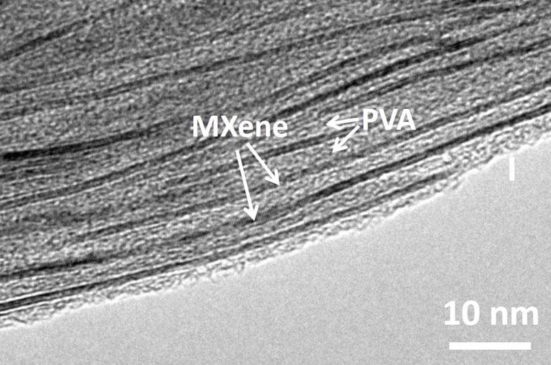
To produce the flexible conductive polymer nanocomposite, the researchers intercalated the titanium carbide MXene, with polyvinyl alcohol (PVA) –a polymer widely used as the paper adhesive known as school or Elmer’s glue, and often found in the recipes for colloids such as hair gel and silly putty. They also intercalated with a polymer called PDDA (polydiallyldimethylammonium chloride) commonly used as a coagulant in water purification systems.

“The uniqueness of MXenes comes from the fact that their surface is full of functional groups, such as hydroxyl, leading to a tight bonding between the MXene flakes and polymer molecules, while preserving the metallic conductivity of nanometer-thin carbide layers.  This leads to a nanocomposite with a unique combination of properties,” Gogotsi said.

The results of both sets of MXene testing were recently published in the Proceedings of the National Academy of Sciences. In the paper, the researchers report that the material exhibits increased ability to store charge over the original MXene; and 300-400 percent improvement in strength.

“We have shown that the volumetric capacitance of an MXene-polymer nanocomposite can be much higher compared to conventional carbon-based electrodes or even graphene,” said Chang Ren, Gogotsi’s doctoral student at Drexel. “When mixing MXene with PVA containing some electrolyte salt, the polymer plays the role of electrolyte, but it also improves the capacitance because it slightly enlarges the interlayer space between MXene flakes, allowing ions to penetrate deep into the electrode; ions also stay trapped near the MXene flakes by the polymer. With these conductive electrodes and no liquid electrolyte, we can eventually eliminate metal current collectors and make lighter and thinner supercapacitors.”

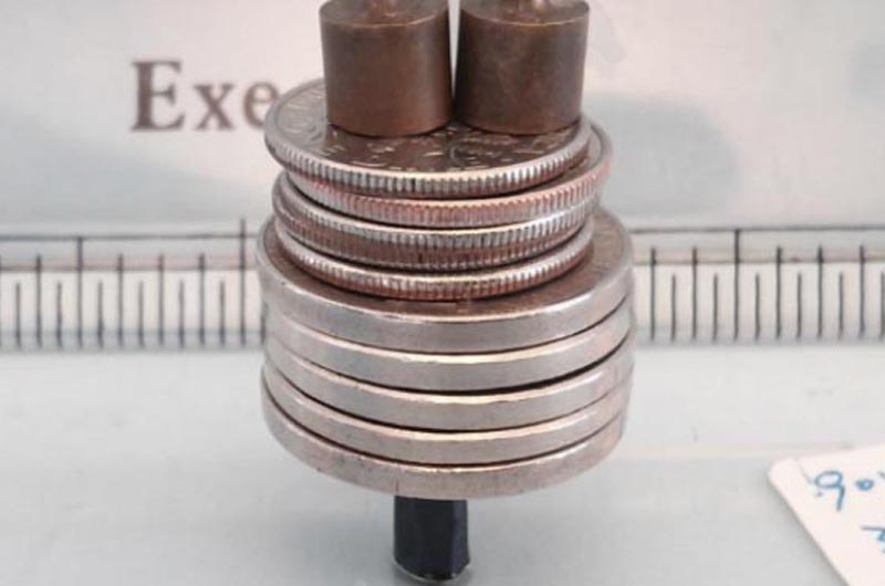
Though just a few atoms thick, the MXene-polymer nanocomposite material shows exceptional strength -especially when rolled into a tube.


The testing also revealed hydrophilic properties of the nanocomposite, which means that it could have uses in water treatment systems, such as membrane for water purification or desalinization, because it remains stable in water without breaking up or dissolving.

In addition, because the material is extremely flexible, it can be rolled into a tube, which early tests have indicated only serves to increase its mechanical strength. These characteristics mark the trail heads of a variety of paths for research on this nanocomposite material for applications from flexible armor to aerospace components. The next step for the group will be to examine how varying ratios of MXene and polymer will affect the properties of the resulting nanocomposite and also exploring other MXenes and stronger and tougher polymers for structural applications.