Tag Archives: memory

KRISHNASWAMY RAMKUMAR, VENKATRAMAN PRABHAKAR and RAVINDRA KAPRE, Cypress Semiconductor Corp., San Jose, CA

SONOS (Si-Oxide-Nitride-Oxide-Si) based eNVM technology is well-suited for System-On-a Chip (SOC) products as they are very compatible with standard logic/mixed-signal CMOS process flow. This paper describes how the SONOS based eNVM technology has been successfully developed and scaled down to 28nm node. With the shrink, SONOS has been seamlessly integrated into advanced front-end process flows with novel features such as stress enhancement techniques and High K-Metal Gate. Process/integration innovations have enabled the design rule shrink by minimizing the Vt variations of the memory cell devices in-spite of enhanced impact of dopant fluctuations. In addition, optimizations of the SONOS gate stack also have enabled the memory to have very high reliability even with scaling.

Why SONOS?

Critical factors for the choice of the NVM technology for an embedded memory include the cost of integration and the extent of its impact on the baseline CMOS device performance. SONOS is superior in both respects due to the simplicity of its integration (fewer extra lithography masks) as shown in FIGURE 1 and the minimal impact on CMOS device performance (FIGURE 2) which means baseline device models are not affected by the integration. This gives a significant edge to SONOS for multiple product applications.

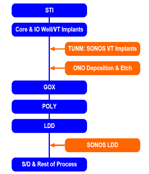
FIGURE 1. Typical process flow for SONOS integration.

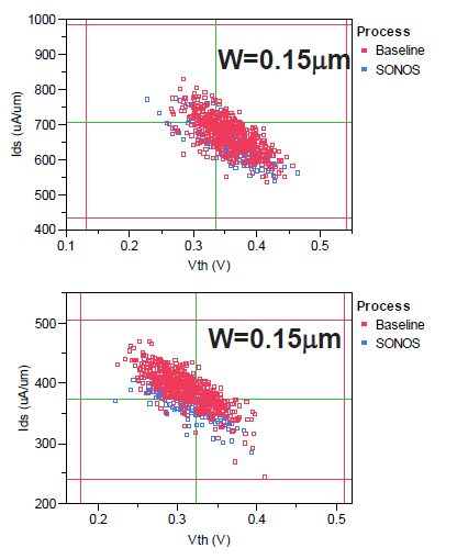
FIGURE 2. Device performance matching.

SONOS eNVM cell

A SONOS device structure and 2T-SONOS cell are schematically shown in FIGURE 3.

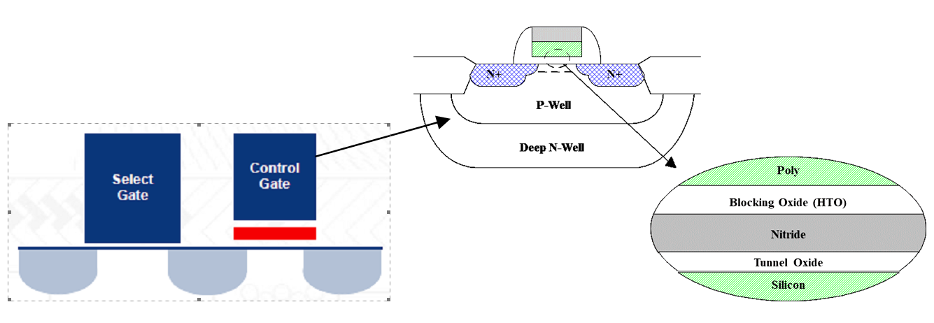
The cell consists of a SONOS Control Gate (CG) in series with a CMOS Select Gate. Structurally both are MOSFETs with the CG having a ONO gate dielectric and SG having a SiO2 or High K based gate dielectric. The CG is the memory device in which charge injected from the Si substrate across the thin tunnel oxide by Fowler-Nordheim tunneling is trapped in the Nitride (N) layer of the ONO stack. The charge can be either Positive (hole trapping) or negative (electron trapping) depending on the polarity of voltage applied to the gate. The trapped charge changes the threshold voltage (Vt) of the CG between a “Program (VTP)” and an “Erase (VTE)” state. The difference in Vt between the program and erase staes defines the memory window.

SONOS memory cell performance

The program/erase efficiency of a SONOS memory cell determines how well it can be programed or erased. The Vts and Vt window are determined by the voltage appled across the ONO dielectric of the CG and the time duration of the program/erase pulse. The reliability of the memory cell defines its ability to maintain window enough to sense the two states clearly during the entire life of the memory. The initial window is maximized by optimizing the SONOS stack and program/erase conditions using the progamming  curves which show how the VTP and VTE vary wit program/erase pulse width (FIGURE 4a).

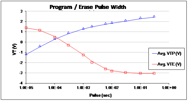
FIGURE 4. Program-Erase characteristics of SONOS cell with (a) Normal and (b) thicker top oxide.

The saturation in the VTE clearly indicates that the charge in the nitride, during erase, stops increasing because the additional hole charge injected from the substrate is compensated by the electron charge injected from the gate to the nitride. The injection from the gate is determined by the thickness and quality of the top oxide. Thinner or poor quality top oxide leads to increased injection from gate and shows increased erase saturation while a physically thicker top oxide drastically reduces injection from gate and hence results in much lower erase saturation (FIGURE 4b).

Endurance and Data Retention are the most critical specifications for a NVM and these reliability requirements are becoming more stringent as embedded NVM products are getting into new markets such as automotive electronics. SONOS typically has good endurance performance (FIGURE 5a). With the engineering of a unique, proprietary ONO stack, robust retention performance has been achieved for all Cypress products (FIGURE 5b). On certain integration flows, SONOS eNVM can meet automotive retention specs.

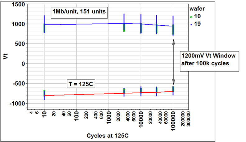
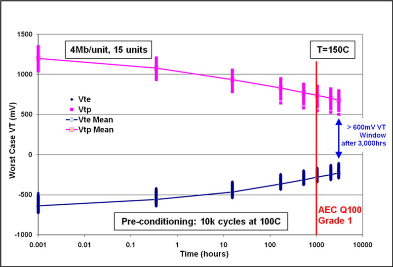
FIGURE 5. SONOS Reliability – (a) Endurance (b) Retention.

SONOS cell scaling – Vt uniformity

To meet the ever increasing demand for larger memories, the SONOS memory cell is shrunk by moving to more advanced technologies to take advantage of tighter design rules. Cell size trend with technology nodes, demonstrated on Silicon, is shown in FIGURE 6 for two types of SONOS cells, Dedicated Source Line (DSL) and Common Source Line (CSL).

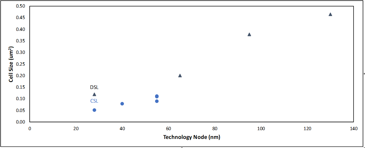
FIGURE 6. Trend of SONOS cell size.

The key challenege for the shrink is the degradation of Vt uniformity on account of increased impact of Random Dopant Fluctuations (RDF) at the surface of the channel of the SONOS device. This can be due to the inherent effect of dopants enhanced by diffusion of dopants during high temperature steps. For successful shrink, several process modifications, especially reduction of dopants in the surface of the channel of CG and use of deeper channel implants with heavier species such as Indium is required so as to keep surface dopant concentrations low. In addition, doping by species such as Carbon can reduce the transient enhanced diffusion of channel dopants. Reduction in thermal budget after SONOS stack formation also lowers the diffusion of dopants to the surface and hence reduces RDF. With the use of such techniques, the Vt sigma can be kept reasonably low with technology shrink as shown in FIGURE 7.

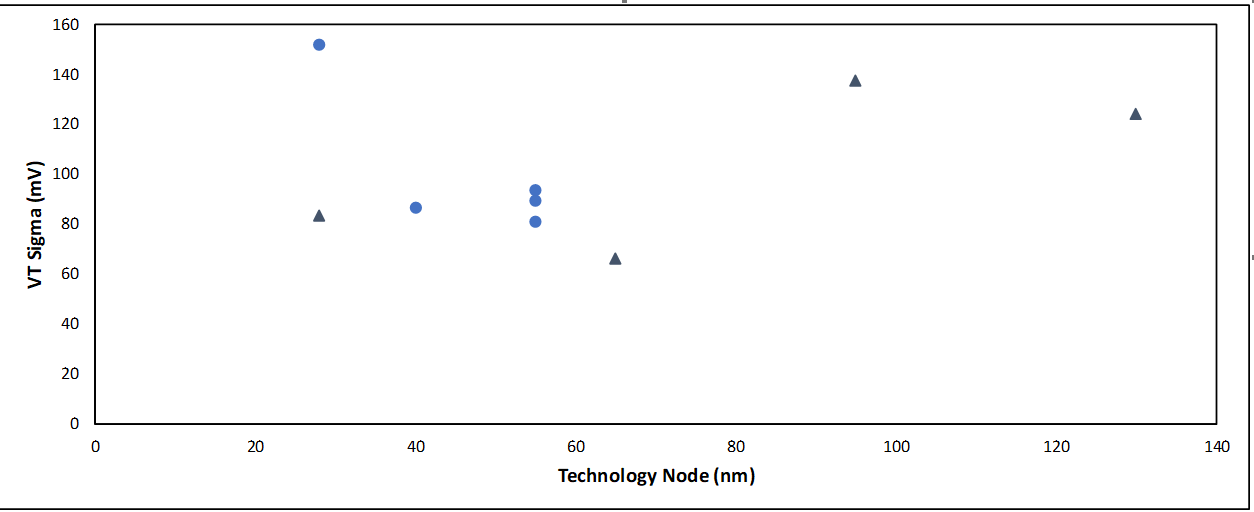
FIGURE 7. Vt sigma trend with technology shrink.

The impact of new doping strategies on maintaining a low Vt sigma is clearly seen in this trend which shows how process optimizations lowers sigma in all technology nodes. At the beginning of technology development such as in 28nm node, the sigma is typically high. With process and /or cell optimizations, the sigma becomes lower. A typical example of Vt sigma improvement with reduction in the diffusion of dopants to the surface of channel of CG is shown in FIGURE 8 below.

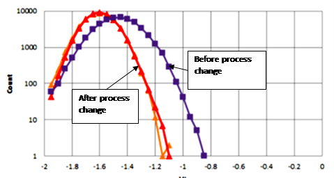
FIGURE 8. Vt sigma improvement.

Maintaining a low sigma greatly helps to minimize the flash yield loss due to widening of Vt distribution at Beginning of Life (BOL) and at End of Life (EOL), typically after a high temperature bake.

SONOS integration into High K-Metal gate process flow

With the transition of CMOS technology to High K-Metal Gate (HKMG) at 28nm node and beyond, it is imperative that SONOS be compatible with HKMG. This has been demonstrated at 28nm node with an integration approach that has the HK dielectric as part of the top oxide of the ONO stack and the MG as the gate of the CG. This is a true integration of HKMG into SONOS device and enables embedded memory products in very advanced technology nodes. Endurance and retention curves for a SONOS cell with HKMG (FIGURE 9) show that robust reliability can be achieved with a greatly shrunk NVM cell.

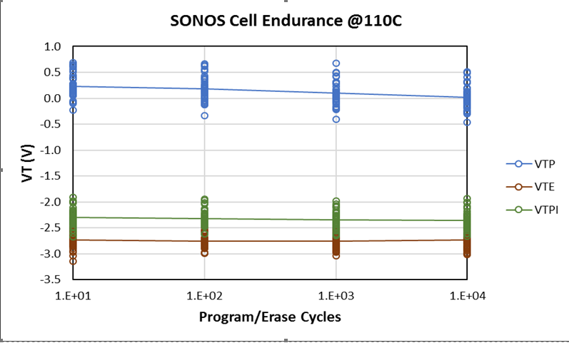
FIGURE 9. Endurance and Retention of SONOS cell integrated into High K-Metal Gate process flow.

Figure 9b.

SONOS for analog NVM

Analog memory is emerging as a strong candidate for “AI edge” applications. Analog NVM uses NVM array with all WLs turned on in 1 block to sum currents. Power needed for making an “inference” is ~1000X lower using analog NVM compared to GPU. Applications are in speech processing, image processing etc. without uploading to the cloud. The memory has multiple levels (8 or 16) and each ID/VT level is a “weight” for the inference and 16 levels can give very low error rates.  ~1-3% overlap of distributions between neighboring VT levels is acceptable.

Key requirements for analog memory for AI edge are

  1. 8 to 16 ID/VT levels between 1E-11A to 1E-5A (lower current levels improve power efficiency)
  2. To achieve ~1-3% overlap of distributions we need levels to be ~5sigmas apart (peak to peak)
  3. Uniform subthreshold slope is preferred, otherwise there is larger error in targeting different ID levels
  4. 1K cycles endurance is sufficient; cycle-to-cycle stability in ID is required (no issue for SONOS)
  5. Refresh of weights possible once a year (1 year at 55C retention is acceptable)
  6. Program time of whole array is a concern

SONOS is a very promising option for the analog memory with multiple levels due to the low Vt sigma. This can be achieved by programming / erasing the SONOS cell to different but distinct Vt or Cell current values, separated by gaps required to sense them as different states of the memory. Soft program or erase is used to place the memory cell at distinct target Vt/Id values with a tight distribution. An illustration of this concept, achieved on test structure arrays is shown in FIGURE 10.

FIGURE 10. Multiple Vt (left) or Id (right) levels of analog SONOS memory.

Although this data is preliminary, it shows that SONOS array can be used for analog memory with the right conditions of program/erase.

Conclusions

It is clear from the above sections that SONOS is a very strong option for eNVM in all advanced nodes, the key advantage being the simplicity of integration into a baseline flow. In addition, it seems to be a very good option for analog memory used in AI edge applications.


GOURI SANKAR KAR and ARNAUD FURNEMONT, imec, Leuven, Belgium

Every day, even every second, we produce massive amounts of data. With an estimated annual data growth rate of 1.2 to 1.4x (source: IDC’s Data Age 2025 study, March 2017), the amount of digital data produced in the world will soon exceed 100 zettabyte. To grasp the meaning of this number – we would need to fill a soccer field with terabyte solid state drives (SSDs) stacked 28 meter high if we would want to store all this data. The data are partly generated through well-known applications such as Amazon, YouTube, Facebook or Netflix. But emerging IoT applications will make a significant contribution as well. Examples are the autonomous car (accounting for 4,000GB of data per day), the smart building (>275GB per day, per building) and the smart city (>1000TB per day, per city). Huge amounts of bandwidth are required to transport all this data – from the application to an edge node, then to a base station, and then to a data center – a challenge that is tackled by 5G and optical fiber technologies. Throughout this data flow, stringent requirements will be imposed on memory and storage – in terms of density, bandwidth, cost and energy.

Clever data mining, and reduced energy consumption

At some point in the flow of data transport, the generated data will need to be analyzed and converted into knowledge and wisdom by means of machine learning techniques. The exact point at which this will happen, will significantly impact the requirements on memory and storage. For example, if machine learning can be applied just after data generation, it can help relax the requirements. If, on the other hand, data is turned into wisdom later in the process, more raw data will need to be stored throughout the whole process.

The zettabyte era will also challenge the power that is consumed by the growing amount of data centers, for processing, transporting and storing all the data. If we don’t optimize the energy consumption for these operations, data centers worldwide may use almost 8000 terawatt-hours by 2030 (source: https://www.labs.hpe.com/next-next/energy). That’s about the amount of electricity consumed by Europe, Africa and part of Asia today. In recent years, several technologies have been introduced in the data centers to address power and performance issues for storage, including, for example, the wide deployment of solid state drives since 2014, and the introduction of the first emerging memory technologies in 2017. But to be prepared for the zettabyte era, we will have to introduce novel non-volatile memories with unprecedented density and speed, and improved power consumption.

The slowdown of today’s memory roadmap

Let’s have a closer look at today’s memory landscape (FIGURE 1). Close to the central processing unit (CPU), fast, volatile embedded static random access memories (SRAMs) are the dominant memories. Also on chip are the higher cache memories, mostly made in SRAM or embedded dynamic random access memory (DRAM) technologies. Off-chip, further away from the CPU, you will mainly find DRAM chips for the working memory, non-volatile Flash NAND memory chips for storage, and tapes for long-term archival applications. In general, memories located further away from the CPU are cheaper, slower, denser and less volatile.

FIGURE 1. Application and performance space of the existing conventional memories (HPC = high performance computing; DSP = digital signal processing; ROM = read only memory; duty cycle = the proportion of time during which the memory device is operated).

For half a century, Moore’s Law has driven cost improvement of memory technologies, and this has translated into a continuous increase of the memory density. However, despite large improvements in memory density, only storage density (Flash NAND devices and tapes) has truly kept pace with the data growth rate. With the transition from NAND to 3D-NAND devices, density improvement for this storage class is however expected to slow down as well, and go below the data growth rate soon.

Unlike in logic development – which has always been driven by improvements in cost and device physics – improving the power/performing benefits for memory has barely been taken care of. As a result, energy reduction and speed improvement are far from following up the data growth rate, for both memory and storage devices (FIGURE 2).

FIGURE 2. Growth rates for the main memory roadmaps; (red) only storage density has kept pace with the data growth rate.

Emerging technologies to the rescue?

To meet the memory requirements of the zettabyte era (i.e., improved density and speed, and reduced energy consumption), imec is exploring multiple emerging memory options, for standalone as well as for embedded applications (FIGURE 3). Options range from MRAM technologies for cache level applications, new ways for improving DRAM devices, emerging storage class memories to fill the gap between DRAM and NAND technologies, solutions for improving 3D-NAND storage devices, and a revolutionary solution for archival type of applications. Below, we review their status and challenges, and investigate whether these emerging memory roadmaps can cope with the zettabyte world.

FIGURE 3. Memory research landscape at imec – application and performance space.

MRAM technologies for embedded cache level applications

Spin transfer torque MRAM (STT-MRAM) technology has emerged as a candidate technology for replacing L3 cache embedded SRAM memories. It offers non-volatility, high density, high speed and low switching current. The core element of an STT-MRAM device is a magnetic tunnel junction in which a thin dielectric layer is sandwiched between a magnetic fixed layer and a magnetic free layer. Writing of the memory cell is performed by switching the magnetization for the free magnetic layer, by means of a current that is injected perpendicular into the magnetic tunnel junction.

Because of this geometry, the read and write operations are performed through the same path, and this challenges the reliability of the device. These reliability issues in combination with increased energy at sub-ns switching speeds make STT-MRAM memories unsuitable for replacing the faster L1/L2 cache SRAM memories.

An MRAM variant, the spin orbit torque MRAM (SOT-MRAM), can overcome these issues. In these devices, switching the free magnetic layer is done by injecting an in-plane current in an adjacent SOT layer, as such de-coupling the read and write path and improving the device endurance and stability. Imec recently demonstrated the ability to fabricate state-of-the-art SOT-MRAM devices on 300mm wafers using CMOS compatible processes (FIGURE 4). The devices exhibited an unlimited endurance (>5×10¹⁰), fast switching speed (240ps), and power consumption as low as 300pJ. We also explore ways for further reducing energy consumption, by bringing down switching current and demonstrating field-free switching.

FIGURE 4. (Left) SOT-MRAM device, and (right) SOT switching distribution as a function of pulse voltage for various pulse lengths.

An imec view on DRAM scaling

DRAM is structurally a very simple type of memory. A DRAM memory cell consists of one transistor and one capacitor, that can be either charged or discharged. Traditionally, double-sided cylindrical capacitor structures have been used, with a dielectric material contained inside as well as outside the capacitor structure. However, when spacing becomes smaller, we need to increase the aspect ratio of these structures – since a certain amount of capacitor area is needed to maintain the memory’s performance. For very large aspect ratios, these DRAM structures are fabricated at the limits of mechanical stability. The industry may therefore transition to a new capacitor architecture: the high-aspect ratio one-pillar architecture, with the dielectric film now only on the outside (FIGURE 5). This change may make it possible to use thicker films of higher-k dielectrics, which in turn will allow reducing the aspect ratio of the one-pillar structure and improving leakage. A new dielectric with these specifications is currently under development at imec.

FIGURE 5. An imec view on the DRAM scaling roadmap; inset: impact of the one-pillar capacitor architecture

Further down the road, we are investigating if we can place the peripherical logic directly under the array of capacitors and transistors. This logic circuitry controls how data is moved to and from the memory chip, and typically consumes considerable area. Today, the transistor of the DRAM memory cell is however built on silicon. To be able to move the peri logic underneath the DRAM array, we need to replace this transistor with a non-Si transistor that is back-end compatible. At imec, we are moving towards a thin-film indium gallium zinc oxide (IGZO)-based transistor (FIGURE 6). This architecture is expected to give us one generation of Moore’s law scaling. In addition, it will enable ultimate 3D DRAM integration as well.

FIGURE 6. Novel oxide semiconductor based DRAM cell transistor.

Emerging memory and selector concepts for storage class memory

Storage class memory has been introduced to fill the gap between DRAM and NAND Flash memories in terms of latency, density, cost and performance. This new memory class should allow massive amounts of data to be accessed in a very short time. Most probably, more than one novel memory technology will be required to span the entire gap. The imec team explores several emerging technologies for storage class memory, including various cross-point-based architectures for the memory element, such as phase-change-RAM (PC-RAM), vacancy-modulated conductive oxide (VMCO), conductive bridging RAM (CB-RAM) and oxide RAM (OxRAM). When it comes to high-density applications, all these memory elements require two-terminal selector elements that connect serially with each of the memory elements. These selector elements suppress the sneak currents that run through the unselected cells in the cross-point array during memory operation. Imec is developing GeSe-based ovonic threshold switching (OTS) selector devices that fulfill the requirements imposed by high-density storage class memories, including high thermal and electrical stability, high current density and low off-state current.

Close to the DRAM side of the DRAM-NAND gap, high-density, high-speed MRAM offers an interesting, scalable alternative for the memory element. As this technology requires a selector as well, imec is working on a diode-based selector for this type of device. And finally, closer to the NAND Flash side, a ferroelectric memory based on hafnium-oxide (HfO) has gained interest. Compared to NAND-Flash, this emerging memory can operate at lower voltages and is much faster (with speeds down to 100ns). The easy cell structure can be fabricated with CMOS compatible processes and can be built in a 3D architecture.

3D NAND… and beyond?

Since its introduction several years ago, 3D NAND has become a mainstream storage technology because of its ability to significantly increase bit density. This is enabled by transitioning from 3 bits per cell to 4 bits per cell. And, instead of traditional x-y scaling in a horizontal plane, 3D NAND scales in the z direction by stacking multiple layers of NAND gates vertically. Today, stacking over 60 layers has become possible. However, increasing the numbers of layers challenges the deposition and etch processes. Also, the more layers that are stacked, the more stress evolves inside the layers, and this can cause a collapse of the 3D NAND pattern – a challenge that is tackled by imec. Imec also investigates alternative channel materials and processes – such as a silicon macaroni channel – that can overcome the limitations of the traditionally used poly-Si channels.

Despite all these advances, the density improvement of 3D NAND is expected to slow down and go below data growth rate soon. Therefore, the search for an emerging memory technology that is faster and cheaper than 3D NAND is ongoing. So far, there are no good candidates out there that can beat the 3D NAND density, especially because of the outstanding capability of 3D NAND Flash technology to integrate 3-4 bits per cell.

DNA storage: the holy grail of archival storage?

Imagine that we could store all data of the world in a container the size of a car, and store them for a very long time? That is exactly what DNA storage promises. DNA can be kept stable for millions of years – today, it is still possible to extract DNA from the woolly mammoth – guaranteeing long term retention. DNA as a medium for storage is also extremely dense and compact. Writing can be performed by encoding binary data onto strands of DNA through the process of DNA synthesis. The DNA strand can be built up with the base pairs representing a specific letter sequence, through a series of deprotection and protection reactions. As from the read side, there is an enormous technology push to sequence DNA faster and faster and at lower cost. Progress in DNA sequencing has been amazing, even outpacing Moore’s law. But researchers still have a long way to go before reasonable targets (1Gb/s) can be reached. To realize this, faster fluidics, faster chemical reactions and much higher parallelism are needed than what’s possible today. At imec, we work towards faster write/read operation, and towards making DNA storage a cost-effective solution for long-term storage.

Towards a sustainable zettabyte era

It has become clear that the classical memory roadmap cannot handle the zettabyte world in terms of energy, density, speed and cost. As shown above, imec is working on several emerging memory and storage technologies that can largely improve on density, system performance, and, partly, speed. However, energy consumption remains the biggest challenge towards a truly sustainable zettabyte era. And this highlights the need to continue collaborating with academia and industry on reduced energy consumption for memory technologies.

Talking about sustainability brings another aspect of the zettabyte era to mind: recycling. To be able to process and store all the data, massive amounts of devices will be produced. The advent of emerging technologies will also bring in new materials, which today are hardly recycled. To enable a truly sustainable zettabyte era, the semiconductor industry should therefore also find ways to improve the recyclability of all these materials.

GOURI SANKAR KAR is distinguished member technical staff emerging memories, and ARNAUD FURNEMONT is memory director at imec, Leuven, Belgium.

Editor’s Note: This article was originally published in the October 2018 issue of Solid State Technology.