Tag Archives: Small Times Magazine

May 23, 2011 — The UK National Physical Laboratories (NPL) scientists, in collaboration with Linköping University, Sweden, discovered that electrostatic force microscopy (EFM) can be used to identify graphene thicknesses under ambient conditions. The technique more accurately measures epitaxially grown graphene thickness on SiC wafers than traditional optical microscopy.

Figure. The left hand image is the topography; the middle the topography error image; and right the electrostatic force microscopy image where the tip bias has been switched half way through the image.

Optical microscopy identifies exfoliated graphene sheets up to ~100μm in size. For epitaxial graphene grown on silicon carbide (SiC) wafers, the nanomaterial’s thickness is difficult to determine with standard tools. EFM scanning probe microscopy is able to clearly identify different graphene thicknesses. The technique can also be used in ambient environments applicable to industrial requirements.

Thicker graphene sheets share common aspects with the bulk material graphite. Thin graphene sheets, such as 1 or 2 layers, have nano-induced properties. For semiconductor and photovoltaics device applications, one- and two-layer graphene needs to be precisely identified apart from the substrate and regions of thicker graphene.

The NPL/Linköping University work was recently published in Nano Letters. Access the article here: http://pubs.acs.org/doi/abs/10.1021/nl200581g

Learn more at www.npl.co.uk

Follow Small Times on Twitter.com by clicking www.twitter.com/smalltimes. Or join our Facebook group

May 23, 2011 — The National Institute of Standards and Technology (NIST) George Mason University (GMU) researchers are studying the optimal characteristics of silicon nanowires and dielectric stacks for charge-trapping memory. The resultant charge-trapping memory devices will offer lower power consumption and faster NVM operation, targeting portable computers and cell phones that operate longer between charging sessions.

NIST’s measurement capabilities were used to determine the best way to design charge-trapping memory devices based on nanowires, which must be surrounded by thin dielectric layers that store electrical charge. Software modeling and electrical device characterization led the NIST and GMU team through a range of dielectric structures to optimize device design.

Figures. In this schematic (top) and transmission electron micrograph (TEM image, bottom), a Si nanowire is shown surrounded by a stack of thin dielectric layers. NIST scientists determined the best arrangement for this dielectric stack for the optimal construction of silicon nanowire-based memory devices. Credit: Schematic: Zhu, GMU. TEM: Bonevich, NIST.

20nm-diameter silicon nano wires form a non-volatile memory (NVM) architecture, retaining contents while power is off, much like flash memory devices. Nanowire memory devices hold an additional advantage over flash memory, which is unsuitably slow for local cache memory in the central processor. "Cache memory stores the information a microprocessor is using for the task immediately at hand," says NIST physicist Curt Richter. "It has to operate very quickly, and flash memory just isn’t fast enough."

Qiliang Li, assistant professor of Electrical and Computer Engineering at GMU, expects their findings to create a platform for more experimenters to further investigate the nanowire-based approach to high-performance NVM, leading to real applications of nanowire-based memory.

Results are published in the journal Nanotechnology:
X. Zhu, Q. Li, D. Ioannou, D. Gu, J.E. Bonevich, H. Baumgart, J. Suehle and C.A. Richter. Fabrication, characterization and simulation of high performance Si nanowire-based non-volatile memory cells. Nanotechnology, May 16, 2011, 22 254020 doi: 10.1088/0957-4484/22/25/254020. Access the article here: http://iopscience.iop.org/0957-4484/22/25/254020 
 
The National Institute of Standards and Technology (NIST) is an agency of the U.S. Department of Commerce. Learn more at http://www.nist.gov/index.html

May 23, 2011 — SiTime Corporation, an analog semiconductor company, launched the SiT820X family of MEMS-based programmable oscillators for telecom, networking, storage and wireless applications. The SiT820X family consists of the SiT8208 and SiT8209 programmable oscillators that operate from 1 to 80MHz and 80 to 220MHz respectively. They are fabricated with SiTime’s MEMS and analog semiconductor technologies and offer drop-in replacements for quartz, SAW, and overtone oscillators.

The new MEMS oscillators claim unprecedented jitter performance; 600 Femtoseconds of integrated RMS phase jitter measured from 12kHz to 20MHz. These devices achieve 2x better stability over the industrial temperature range than quartz-based solutions, the company reports.

Programmable features enable over 200 part numbers, each of which can be a drop-in replacement for existing quartz, SAW or overtone oscillators.
 
The SiT8208 and SiT8209 feature:

  • 600 Femtoseconds of typical integrated RMS phase jitter (measured per SONET-specified 12 kHz to 20 MHz range)
  • Any frequency with 6 decimal places of accuracy
  • Frequency stability as low as ±10PPM for enhanced system reliability against the effects of spurious noise
  • Programmable drive strength for impedance matching and EMI reduction
  • High-drive options that can be used to drive multiple loads
  • Available in industry standard 3225, 5032 and 7050 packages
  • Industrial (-40 to +85°C) and commercial temperature (-20 to +70°C) operation
  • 1.8V and 2.5-3.3V operation

Samples of the SiT8208 and SiT8209 will be available in early June 2011 with production in Q3 2011. SiTime ships customized samples in one week and production quantities in 3-5 weeks.

SiTime Corporation, an analog semiconductor company, offers MEMS-based silicon timing solutions that replace legacy quartz products. Learn more at www.sitime.com

Also read: SiTime enters resonator market with MEMS resonator for real-time clock and time-keeping apps

Follow Small Times on Twitter.com by clicking www.twitter.com/smalltimes. Or join our Facebook group

May 19, 2011 — The MF3 Microfluidics Consortium, which includes Philips, STMicroelectronics (STM) and others, recognizes a need for standards in how microfluidic chips are connected to systems. Since microfluidics perform diverse tasks, three main interconnect types were identified: high temperature/pressure, electrical/optical interconnects to chip holders, and disposable chip interconnects. The consortium will first tackle high-temperature/pressure.

The MF-3 Microfluidic Consortium comprises a group of companies including SonyDADC, Philips, ST-Microelectronics, Biocartis, Dolomite and Micronit.

The industrial and consumer use of microfluidic solutions in components and instruments is hampered by the lack of standardized interconnects, says the MF-3 Microfluidic Consortium. General adoption of microfluidics will only be possible with an agreement on standardized interconnects between chips and systems.

Microfluidics are more diverse than conventional electronics and different applications will need different classes of interconnect. Multinational and SME Members of the MF3 consortium have put forward suggestions for addressing a variety of applications for microfluidic interconnects. The MF-3 Microfluidic Consortium has divided the requisite interconnect schemes into three groups:

At the consortium’s recent meeting in Milan, a draft proposal for higher temperature/ pressure interconnects was accepted and will be published shortly.

The MF3 consortium is now calling for further expressions of user requirements for microfluidic interconnects. These proposals will be discussed in workshops organized by the Consortium later this year.

The MF3 Microfluidics Consortium brings together stakeholders from all parts of the value chain with a shared interest in growing the market for microfluidics-enabled solutions to challenges in healthcare, environment and beyond. The consortium was launched in June 2008 and is open for further members worldwide. For more information, visit www.microfluidicsinfo.com

Follow Small Times on Twitter.com by clicking www.twitter.com/smalltimes. Or join our Facebook group

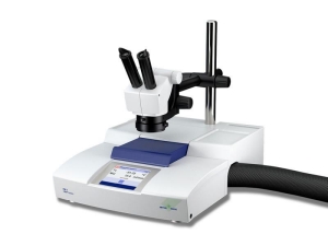
May 19, 2011 — METTLER TOLEDO launched the Flash Differential Scanning Calorimeter (FDSC), which enables materials studies over a temperature range from -95ºC to +450ºC in one measurement.

Click to EnlargeScientists can use the tool to evaluate crystallization and reorganization processes of materials, for example, how materials respond to rapid cooling in modern high-speed production processes. The FDSC operates at extremely high cooling (-4,000ºC/sec) and heating (40,000ºC/sec) rates. Very fast cooling and heating rates allow researchers to generate material under real process conditions (on cooling) and then measure those material properties (on heating).

The Flash DSC 1 opens the door to the wider experimental parameters required to investigate the meta-stable and time-dependent transitions of materials.

METTLER TOLEDO is a global manufacturer of precision instruments. Additional information about METTLER TOLEDO can be found at www.mt.com.

Follow Small Times on Twitter.com by clicking www.twitter.com/smalltimes. Or join our Facebook group

May 18, 2011 — Conventional ICs are rigid, planar, and brittle. Current flex circuit laminate/metal/laminate structures limit performance and circuits suffer broken interconnects after repeated flexing. The holy grail of flexible electronics would combine the performance of ICs with a form factor that could be stretched, twisted, and conformed to unconventional shapes. David Icke, CEO, MC10 Inc. spoke about flexible electronics in his ConFab Emerging Technologies talk, "Electronics Anywhere: Conformal, Stretchable Electronics Technology & Applications."

Icke discussed flexible silicon nanoribbons that use familar wafer fab processes (think etch, encapsulation) in new IC concepts. "Acordian physics" allow these ribbons to bend and twist without compromising reliability. Conformal polymeric substrates are also in use to reduce stress on the electronics during stretching or twisting, or combinations of movement. The wavy design of Si nanoribbons absorbs strain during excursions (see figure), cushioning the active micro-CMOS "chip" elements. A neutral mechanical plane also limits strain.

The process that Icke described is compatible with conventional foundry equipment and processes, and promises low cost with high yields. >GHz performance is acheivable. The process could ramp for electronics, as well as photovoltaics, LEDs, thin-film batteries, thermoelectric devices, piezoelectrics, sensors, etc.

The electronics can be patterned on unusual substrates (leather, for instance) and shapes (how about a golf ball?). Bending mechanics and interconnect designs are modeled and optimized to accommodate desired configurations and geometries. New flexible electronics can interface with users in revolutionary ways — integrating with the eye or skin, or implanted into the body. Accepted form factors and IC lifetimes, power consumption are not restraints.

Icke shared some ideas for the technology’s application: human-integrated electronics, wearable energy sources, advanced curved imagers, and many other options.

More from the ConFab:


May 18, 2011 – GLOBE NEWSWIRE — Northrop Grumman Corporation (NYSE:NOC), in partnership with the Georgia Institute of Technology, will develop a new type of microelectromechanical systems (MEMS) gyroscope technology for the Defense Advanced Research Projects Agency’s (DARPA) Microscale Rate Integrating Gyroscope program.

Utilizing a new MEMS fabrication process, the Northrop Grumman-led team will produce a proof-of-concept micro gyro that can perform as well as current silicon MEMS devices in a smaller size, lighter weight, and lower power package.

"The Northrop Grumman and Georgia Tech team will [enable] the extreme miniaturization of highly stable navigation devices, with small energy dissipation," said Farrokh Ayazi, a professor in the School of Electrical and Computer Engineering (ECE) at Georgia Tech. Dr. Ayazi is a principal investigator for this project and serves as co-director for ECE’s Center for MEMS and Microsystems Technology.

The MEMS technology developed by Northrop Grumman and Georgia Tech during the initial 12-month award period will form the basis for a micro resonator gyro capable of achieving navigation-grade performance. The new MEMS fab process will enable gyros for unmanned vehicles to handheld devices, Charles Volk, vice president and chief technology officer of Northrop Grumman’s Navigation Systems Division.

DARPA’s Microscale Rate Integrating Gyroscope program seeks to develop miniature navigation-grade gyros for use in personal navigation, unmanned vehicle navigation, GPS denied/challenged locations, and other size and power constrained applications requiring precision navigation. Northrop Grumman, in partnership with Georgia Tech, was awarded a research and development contract for the preliminary design, development and testing of micro-resonator devices.

Northrop Grumman produces navigation products using fiber-optic gyro-based systems, Northrop Grumman’s exclusive hemispherical resonator gyro, unique ZLG gyros, spinning mass gyros, ring laser gyros and micro-electro-mechanical-system gyros, among other technologies. Please visit www.northropgrumman.com for more information.

The Georgia Institute of Technology is one of the world’s premier research universities. The Institute offers research opportunities to both undergraduate and graduate students and is home to more than 100 interdisciplinary units plus the Georgia Tech Research Institute. www.gatech.com

Also read: Introduction to MEMS gyroscopes

May 17, 2011 — The Binnig and Rohrer Nanotechnology Center opened at IBM (NYSE: IBM) Research – Zurich. with 600 guests from industry, academia, and governments. ETH Zurich, a European science and engineering university, and IBM have collaborated for 10 years on nanoscience. Now, the Center will allow scientists from IBM and the university to research novel nanoscale structures and devices to advance energy and information technologies. EMPA, a Swiss national research institution under the umbrella of the ETH domain, also is a partner in the new center.

The Center is named for Gerd Binnig and Heinrich Rohrer, two IBM scientists and Nobel Laureates (1986) who invented the scanning tunneling microscope at the Zurich Research Lab in 1981, thus enabling researchers to see atoms on a surface for the first time. Their work on microscopy tools has allowed researchers to visualize the nanoscale. The two scientists attended today’s opening ceremony, at which the new lab was unveiled to the public. Binnig told Small Times in 2003 that he still recalls what it felt like in 1981 when he tested his technical innovations and saw atomic structures for the first time. "It was like a dream to discover all this," said Binnig, a fellow at IBM Zurich Research Laboratory. "It was like being for the first time on the moon."

Photo. Dr. Paul Seidler, coordinator for the Nanotechnology Center at IBM Research – Zurich stands on the roof of the cutting edge laboratory, which is covered in solar panels. View all the photos from the Center opening here: http://www.flickr.com/photos/ibm_research_zurich/sets/72157626481794199/

The Binnig and Rohrer Nanotechnology Center offers a cutting-edge, collaborative infrastructure designed specifically for advancing nanoscience. The noise-free labs open up a new level of precision, thereby potentially extending the scale on which scientists are able to measure and experiment even further.

A large cleanroom for micro and nanofabrication provides scientists from IBM and ETH Zurich with a flexible environment and tools for lithography, wet processing, dry etching, thermal processes, thin-film deposition or metrology and characterization. The cleanroom also features a special area for processing carbon-based materials and structures.

Six uniquely designed noise-free labs shield extremely sensitive experiments from external disturbances, such as vibrations, electro-magnetic fields, for example from nearby trains and cellphone towers, temperature fluctuations and acoustic noise.

The new Nanotechnology Center has been granted the use of the Minergie quality label, a Swiss standard for sustainable and energy-efficient buildings. Photovoltaics, geothermal probes, and heat recovery windows are part of this efficiency.

The building represents an investment of $60 million in infrastructure costs and an additional $30 million for tooling and equipment which, including the operating costs, are shared by the partners.*

Scientists and engineers from IBM and ETH Zurich will pursue joint and independent projects, ranging from exploratory research to applied and near-term projects including new nanoscale devices and device concepts as well as generating insights about their scientific foundations at the atomic level. Three ETH professors and their teams have moved into the new building and will conduct part of their research in nanoscience on a permanent base. Even more ETH researchers will benefit from the partnership and be able to use the excellent infrastructure for various projects.

One focus of IBM’s research in the Center is put on exploring the "next switch"– the future building blocks for better, faster and more energy efficient chips and computer systems. For example, IBM scientists are currently exploring semiconducting nanowires to potentially increase the energy efficiency of computing devices by 10 times.  In addition, through novel device concepts, such nanowires-transistors could virtually consume zero energy while in passive or standby mode.

Additional research areas include micro- and nanoelectromechanical systems (MEMS/NEMS), spintronics, organic electronics, carbon-based devices, functional materials, cooling, three-dimensional integration of computer chips, opto-electronics and optical data communication in computers as well as silicon nanophotonics.

Researchers will also explore new approaches for fabricating structures and devices with dimensions down to a few nanometers, such as scanning-probe nanolithography or directed self-assembly, addressing the upcoming challenges for manufacturing at the nanoscale.

In addition to these partnerships, IBM will also collaborate in the Center with scientists from several Lithuanian universities, under a five-year agreement that was signed in September 2010 with the Lithuanian Ministry of Economy and Ministry of Education and Science. This collaboration will focus on integrated photonics and novel photonic materials to create faster computers, improved solar technologies, and nanopatterning security tags for advanced anti-forgery technology.

Throughout 2011, IBM will host the IBM Research Colloquia, convening thought leaders at its global labs to discuss technologies of the future and their potential impact on business and society. The first of these colloquia took place today at IBM Research – Zurich, and featured a dialogue on Nanotechnology and the Future of Computing with IBM Fellows and Nobel Laureates, Drs. Gerd Binnig and Heinrich Rohrer, and talks by Prof. Dr. Achim Bachem of the Julich Research Center on 21st Century Supercomputing; Prof. Dr. Karlheinz Meier, Kirchhoff Institute for Physics at Heidelberg University on Brain Inspired Computing and Prof. Dr. Daniel Loss of the University of Basel on Quantum Computing.

Learn more about the Center at http://www.zurich.ibm.com/nanocenter/factsheet.html

* the investment figure is based on an average conversion rate with Swiss Francs (CHF) between April 2008 – April 2011

May 17, 2011 – BUSINESS WIRE — Middle State Tennessee State University has chosen the TESCAN LYRA 3 FIB-SEM workstation to enhance interdisciplinary research. The LYRA 3 FIB-SEM will reside in the MTSU Interdisciplinary Microanalysis and Imaging Center (MIMIC). Operational since 2006, MIMIC is a shared research facility for structural biology and materials science.

The LYRA 3 FIB-SEM workstation combines the TESCAN Wide Field Optics High Resolution Field Emission Scanning Electron Microscope and Focused Ion Beam column (SEM/FEB), providing best in class imaging and 3D material characterization for the most demanding applications. The instrument will be integrated with an EDS (Energy Dispersive Spectrometer) and EBSD (Electron Beam Scanning Diffraction), allowing users to collect chemical and structural information simultaneously during the milling process.

"The LYRA 3 FIB-SEM workstation will not only allow very small structures to be accurately machined, but with specialized, integrated detectors, it can also be used to analyze the structure and chemical composition of a host of sample types, from cross-sections of solar cells to biological specimens," explained Dr. Nathanael Smith, MTSU assistant professor in the physics and astronomy department.

Smith added that the instrument will have 3-D imaging capabilities so that samples will be seen in newer and more powerful ways:

"Applications for the new equipment could include observing the characterization of solar cells (physics); the fabrication of ‘photonic circuits,’ where light is used in place of electricity (physics); and the development of nanomaterials for chemical analysis and catalytic acceleration of chemical reactions (chemistry). Nanotechnology is the study of manipulating matter on an atomic and molecular scale."

The microscopy instrumentation at MIMIC is accessible for research by all MTSU faculty and students. The facilities are also available for fee-based usage by microscopists from industries in the middle Tennessee region.

TESCAN provides scientific instrumentation. Learn more at www.tescan.com

Follow Small Times on Twitter.com by clicking www.twitter.com/smalltimes. Or join our Facebook group

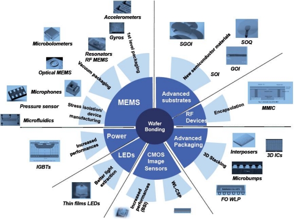
May 17, 2011 Wafer bonding is a complex process, used on 2" to 12" wafers for MEMS, CMOS image sensors, advanced packaging, LEDs, and other chips. Yole Développement published a technology study and market research report, "Permanent wafer bonding," to derive trends in the market and technology through 2016. The report aims at analyzing the market perspectives and technical trends for permanent bonding.

Yole Développement has estimated that the wafer bonding market will grow significantly for the next year. The growth will be driven small-size wafers for LEDs and 12" wafers for 3D die stacking and CIS.

The wafer bonding market is a very complex one, crossing different wafer sizes (from 2" to 12"), different applications (MEMS, CMOS image sensors [CIS], LEDs, power devices, RF and advanced packaging), and different bonding technologies (adhesive, anodic, fusion, direct oxide, eutectic, glass frit, metal diffusion).

Click to Enlarge

Wafer bonding is usually defined as a process that temporarily or permanently joins two wafers or substrates using a suitable process. Historically developed for MEMS and then SOI wafers, wafer bonding technology has shifted to non-mainstream IC applications over the last years.

"MEMS has been the first application where wafer bonders have been massively used (the wafer bonding step is mostly used to protect the MEMS sensitive element), explained Dr Eric Mounier, project manager at Yole Développement. MEMS manufacturers are currently shifting from glass frit for eutectic/metal-based bonding, yielding smaller bond frames. Metal direct bonding also provides hermeticity and mechanical stability for many MEMS applications. For example, Nasiri uses eutectic bonding of the MEMS directly on the aluminum layer of the CMOS wafer. This leads to smaller package footprints & package heights. STMicroelectronics’ latest 3-axis accelerometer (LIS3DH) also shows a new sealing technique: gold eutectic sealing allows a dramatic die size reduction.

CMOS image sensors are also a strong wafer bonding application. Up to two different wafer bonding steps can be necessary for next-generation CMOS image sensor fab: one for back-side illumination, the second for wafer-level chipscale packaging (WLCSP). For CIS, the advent of backside illumination (BSI) technology has raised a competition between molecular bonding and adhesive bonding. Here, cost and final application will drive the final technology choice.

Besides MEMS and CIS manufacturing, wafer bonding also can be used for LED and power device fab. In a typical LED active region, spontaneous emission scatters photons in all directions. If the substrate material has a smaller band gap than the active region, approximately half of the light is absorbed in the substrate; significantly reducing device performance. So, one of the manufacturing solutions for photon loss involves bonding a wafer containing an array of devices to another wafer that provides both a reflective surface for maximum light extraction and a heatsink for thermal management.

Companies cited in the report:

Acreo, AML, APM/UMC, Avago, Ayumi, Bosch, Colibrys, Dalsa, Discera, EVGroup, FhG IMS, FLIR, IBM, Icemos, IMEC, IMT, Infineon, Infineon, Invensense, KTH, Leti, Lumileds, MEMStech, Micralyne, Mitsubishi Heavy Industries, Okmetic, Omron, Osram, Qualcomm, Raytheon, RPI, Sand9, Semefab, Sensonor, Silex, SOITEC, STM, SUSS MicroTEC, Tezzaron, TI, tMt, Tohoku University, TowerJazz, Tracit, Triquint, Tronic’s, TSMC, VTI, Xcom, Ziptronix

Over the 5 past years, much attention has been given to wafer bonding for 3D integration of memories, for example, and other die.

Although EV Group (EVG) is the market leader in permanent bonding, the growth of the bonding equipment market is attracting challengers.

Yole Développement’s report analyzes the technical & economical evolution of the permanent wafer bonding process. It gives 2010-2016 market forecasts for permanent bonding, equipment, an overview of the different bonding approaches and equipment players market shares and competitive information, This market & technology report also presents the trends for permanent bonding, wafer-to-wafer (W2W) vs. chip-to-wafer (C2W) analysis for 3D integration. It describes the applications for wafer bonding with main characteristics and challenges.
 
Report author:
Dr. Eric Mounier has a PhD in microelectronics from the INPG in Grenoble. Since 1998 he is a co-founder of Yole Développement, a market research company based in France. At Yole Développement, Dr. Eric Mounier is in charge of market analysis for MEMS, equipment & material. Yole Développement is a group of companies providing market research, technology analysis, strategy consulting, media in addition to finance services. Learn more at www.yole.fr

Subscribe to Solid State Technology/Advanced Packaging.

Follow Advanced Packaging on Twitter.com by clicking www.twitter.com/advpackaging. Or join our Facebook group