Tag Archives: Small Times Magazine

May 17, 2011 — Catalan Institute of Nanotechnology Professor Adrian Bachtold and his research group created resonators from nanoscale graphene and carbon nanotubes (CNT) that exhibit nonlinear damping. This result could lead to supersensitive detectors of force or mass.

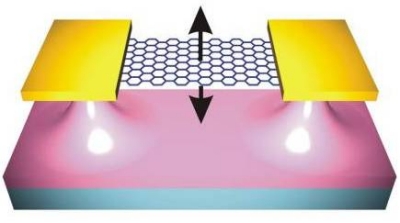
The team formed nanoscale resonators by suspending tiny graphene sheets or carbon nanotubes and clamping them at each end. These devices, similar to guitar strings, can be set to vibrate at very specific frequencies.

Click to Enlarge
Figure. A depiction of the nanoscale mechanical resonators constructed with graphene and CNTs. SOURCE: Catalan Institute of Nanotechnology.

Mechanical resonators mark time in electronic components and stabilize radio transmissions. In all mechanical resonators studied to date, from large objects several metres in size down to tiny components just a few tens of nanometers in length, damping has always been observed to occur in a highly predictable, linear manner.

Bachtold’s research demonstrates that this linear damping paradigm breaks down for resonators with critical dimensions on the atomic scale. The damping is strongly nonlinear for resonators based on nanotubes and graphene, a characteristic that facilitates amplification of signals and dramatic improvements in sensitivity.

Damping is central to the physics of nanoelectromechanical (NEMS) resonators, lying at the core of quantum and sensing experiments. Therefore many predictions that have been made for nanoscale electro-mechanical devices now need to be revisited when considering nanotube and graphene resonators. Prof. Bachtold’s group has achieved a new record in quality factor for graphene resonators and ultra-weak force sensing with a nanotube resonator, using these atomic-level devices.

Results will be published in Nature Nanotechnology (DOI 10.1038/NNANO.2011.71). To retrieve the abstract and full text, visit http://dx.doi.org/ DOI 10.1038/ NNANO.2011.71

Follow Small Times on Twitter.com by clicking www.twitter.com/smalltimes. Or join our Facebook group

May 16, 2011 — Risø DTU researchers, in collaboration with scientists from China and USA, found a new method for revealing a 3D picture of the structure inside a material.

Most solid materials are composed of millions of small crystals, packed together to form a fully dense solid. The orientations, shapes, sizes and relative arrangement of crystals are important in determining many material properties.

Traditionally, it has only been possible to see the crystal structure of a material by looking at a cut surface, giving just 2D information. In recent years, X-ray methods have been developed that can be used to look inside a material and obtain a 3D map of the crystal structure. However, these methods have a resolution limit of around 100nm.

The new technique allows 3D mapping of the crystal structure inside a material down to nanometer resolution, and can be carried out using a transmission electron microscope (TEM).

Figure. 3D mapping of nanometal aluminium film. SOURCE: Riso DTU.

Samples must be thinner than a few hundred nanometers. This will particularly benefit researchers investigating crystal structures inside nanomaterials, where the average crystal size is less than 100nm. The ability to collect a 3D picture of the crystal structure in these materials is an important step in being able to understand the origins of their special properties.

An example of such a 3D map is given in the figure, showing the arrangement of crystals in a 150nm thick nanometal aluminium film. The crystals have identical lattice structure (arrangement of atoms) but they are orientated in different ways in the 3D sample as illustrated by the labels 1 and 2. The colors represent the orientations of the crystals and each crystal is defined by volumes of the same color. The individual crystals of various sizes (from a few nm to about 100 nm) and shapes (from elongated to spherical) are clearly seen and mapped with a resolution of 1nm.

3D mapping allows users to observe the changes taking place inside a material directly. For example, the mapping may be repeated before and after a heat treatment, revealing how the structure changes during heating.

The results are published in the journal Science: Three-Dimensional Orientation Mapping in the Transmission Electron. H. H. Liu, et al. Science 332, 833 (2011). Access the article here: http://www.sciencemag.org/content/332/6031/833.short

The paper is written by scientists from Risø DTU (Denmark), in collaboration with scientists from Tsinghua University (China), Shenyang National Laboratory for Materials Science, IMR (China) and Johns Hopkins University (USA).

The project is funded by Danish National Research Foundation.

Courtesy of Marianne Vang Ryde, http://www.risoe.dtu.dk/.

Follow Small Times on Twitter.com by clicking www.twitter.com/smalltimes. Or join our Facebook group

May 13, 2011 — MIT researchers and their colleagues at the University of Augsburg in Germany discovered a new physical phenomenon that could yield transistors with greatly enhanced capacitance, measured at room temperature. The lanthanum aluminate and strontium titanate composition’s phenomenon could lead to the revival of clock speed as the measure of a computer’s power.

Click to Enlarge
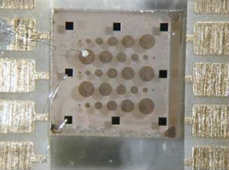
A sample of the lanthanum aluminate-strontium titanate composite, which looks like a slab of thick glass, with thin electrodes deposited on top of it. SOURCE: MIT

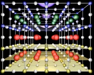
MIT Professor of Physics Raymond Ashoori and Lu Li, a postdoc and Pappalardo Fellow in his lab — together with Christoph Richter, Stefan Paetel, Thilo Kopp and Jochen Mannhart of the University of Augsburg — investigated the unusual physical system that results when lanthanum aluminate is grown on top of strontium titanate. Lanthanum aluminate consists of alternating layers of lanthanum oxide and aluminum oxide. The lanthanum-based layers have a slight positive charge; the aluminum-based layers, a slight negative charge. The result is a series of electric fields that all add up in the same direction, creating an electric potential between the top and bottom of the material.

Ordinarily, both lanthanum aluminate and strontium titanate are excellent insulators. But physicists had speculated that if the lanthanum aluminate gets thick enough, its electrical potential would increase to the point that some electrons would have to move from the top of the material to the bottom, to prevent a polarization catastrophe. The result is a conductive channel at the juncture with the strontium titanate, much like the one that forms when a transistor is switched on. So Ashoori and his collaborators decided to measure the capacitance between that channel and a gate electrode on top of the lanthanum aluminate.

Click to Enlarge
Stacked layers of lanthanum aluminate on layers of strontium titanate, which MIT and University of Ausburg researchers observed creating high capacitance at room temperature.

Although results were somewhat limited by the experimental apparatus, it may be that an infinitesimal change in voltage will cause a large amount of charge to enter the channel between the two materials. "The channel may suck in charge — shoomp! Like a vacuum," Ashoori says. "And it operates at room temperature." While a lot of charge will move into the channel between materials with a slight change in voltage, it moves slowly, much too slowly for the type of high-frequency switching that takes place in computer chips. This could be due to the rough nature of the experimental composition.

The material’s capacitance is so high that the researchers don’t believe it can be explained by existing physics. "We’ve seen the same kind of thing in semiconductors," Ashoori says, "but that was a very pure sample, and the effect was very small. This is a super-dirty sample and a super-big effect."

Capacitance measures how much charge accumulates below a gate for a given voltage. The power that a chip consumes, and the heat it gives off, are roughly proportional to the square of the gate’s operating voltage. So lowering the voltage could drastically reduce the heat, creating new room to crank up the clock.

"For capacitance, there is a formula that was assumed to be correct and was used in the computer industry and is in all the textbooks," says Jean-Marc Triscone, a professor of physics at the University of Geneva, whose group has published several papers on the juncture between lanthanum aluminate and strontium titanate. "What the MIT team and Mannhart showed is that to describe their system, this formula has to be modified."

If researchers can understand the physical phenomena underlying the material’s remarkable capacitance, they may be able to reproduce them in more practical materials.

Triscone cautions that wholesale changes to the way computer chips are manufactured will inevitably face resistance. "So much money has been injected into the semiconductor industry for decades that to do something new, you need a really disruptive technology," he says.

The researchers reported their results in this week’s issue of the journal Science. Access it here: http://www.sciencemag.org/content/332/6031/825.short

May 12, 2011 — JEOL’s atomic resolution transmission electron microscope (TEM), the JEM-ARM200F, rapidly resumes operation after flashing, a routine procedure conducted with any TEM featuring a Cold field emission gun (FEG) source.

Long considered a tradeoff for the higher resolution, higher brightness, and smaller energy spread of a cold FEG TEM, emission stability degrades due to residual gases in the area of the tip. With conventional cold FEG TEMs, the operator must flash every few hours to clean the tip, disrupting operation. 

The JEOL ARM200F Cold FEG TEM offers "Flash & Go," allowing the microscope to resume operation within seconds after flashing, instead of the typical half hour or more that most users of Cold FEG TEMs expect. A newly developed vacuum system effectively evacuates the area around the Cold FEG source to the order of 1 x 10⁻⁹ Pa.

The ARM200F with Cold FEG represents a radical departure from electron optical technology, achieving imaging resolution of 78 picometers with an energy resolution of better than 0.3eV. The higher brightness and narrower energy spread enabled by the Cold FEG are optimized by the ultra stable emission, greatly enhancing atom-atom imaging and chemical analysis.

To see the process, visit www.jeolusa.com/flashandgo.

Follow Small Times on Twitter.com by clicking www.twitter.com/smalltimes. Or join our Facebook group

May 12, 2011 – PRNewswire — STMicroelectronics (NYSE: STM), micro electro mechanical systems (MEMS) supplier, and McGill University collaborated to create an undergraduate course that teaches the integration of multiple state-of-the-art sensors into embedded computer systems. Some 35 students have already completed the course, which started in January 2011.

The new course includes laboratory exercises and a final project that enables students to analyze and design systems that include the integration of data from multiple sensors. It was designed by Professor Zeljko Zilic of the Department of Electrical and Computer Engineering at McGill University and is based around ST’s iNEMO platform, which integrates ST’s most advanced accelerometers, gyroscopes and magnetometers, together with pressure and temperature sensors, to provide 3-axis sensing of linear, angular and magnetic motion, complemented with temperature and barometer/altitude readings.

The course integrates the curricula of computer, electrical and software engineering programs, just as occurs in real-world modern systems design, said Professor Zilic. "For example, smart phones now routinely employ multiple movement sensors to make more effective and intuitive user interfaces, navigation control and position detection and the same technology has unlimited applications in areas as diverse as robotics, factory automation and energy systems."

The course package could be implemented at other universities across North America.

The initial students’ final projects included a gaming application featuring ‘Hidden Markov Model Motion Detection,’ a gesture recognition system for image manipulation, and a tilt-compensated compass with free-fall detection for aircraft use. The next undergraduate course will start in September 2011. In addition, a two-day postgraduate workshop devoted to Integrated Sensor Systems, also based on the iNEMO, will be held at McGill University next week.

Similar collaborative industry/academia courses exist for nanotech, such as the NanoProfessor Program, recently implemented at the University of Calgary.

STMicroelectronics is a global leader serving customers across the spectrum of electronics applications with innovative semiconductor solutions. Further information on ST can be found at www.st.com.

McGill University is a public research university located in Montreal, Quebec, Canada. McGill consistently ranked as the top university in Canada. Learn more at http://www.mcgill.ca/

Follow Small Times on Twitter.com by clicking www.twitter.com/smalltimes. Or join our Facebook group

May 12, 2011 — Researchers from the Technology Integration and Advanced Nano/microsystems (TIAN) Lab at the Department of Mechanical Engineering, University of Minnesota used IC assembly processes to fabricate single-walled carbon nanotube (SWCNT) composite thin film micropatterns and suspended beams. The stiff CNT-polymer composite thin film micropattern and suspended beam have potential applications to novel physical sensors, nanoelectromechanical switches, and other MEMS/NEMS devices.

Lithography-compatible layer-by-layer (LbL) nano-self-assembly was used to assemble negatively charged SWCNTs with a positively charged polydiallyldimethylammonium chloride.

The resultant composite thin film was patterned by oxygen plasma etching with a masking layer of photoresist, resulting in a feature size of 2µm.

The SWCNT nanocomposite stripe pattern with a metal clamp on both ends was released by etching a sacrificial layer of silicon dioxide in the hydrofluoric acid vapor. I-V measurement reveals that the resistance of SWCNT nanocomposite film decreases by 23% upon release, presumably due to the effect of reorientation of CNTs caused by the deflection of about 50nm. A high Young’s modulus is found in a range of 500-800GPa based on the characterization of a fixed-fixed beam using nanoindentation. This value is much higher than those of other CNT-polymer composites due to self-assembly and higher CNT loading.

The group was led by Tianhong Cui at the University of Minnesota. They have studied the lithography-compatible layer-by-layer nano self-assembly process in detail, and has previously configured nanomaterials as thin-film transistors and biosensors. The current work lends itself to nano-switches due to the thin films’ stiffness and electrical conductivity.

Dr Dongjin Lee was a PhD student when the study was conducted. He is currently a postdoctoral associate at the Korea Advanced Institute of Science and Technology (KAIST), Korea. The research group, TIAN Lab, is led by Prof. Tianhong Cui. The research goal of the group is to investigate the fundamental electrical and mechanical principles of new materials for MEMS/NEMS and low-cost micro/nanomanufacturing approaches, utilizing nanotechnology to effectively enhance the performance of micro/nanosystems. Learn more at http://www.me.umn.edu/labs/tianlab/.

Additional information including a detailed version of the fabrication procedure is available in the journal Nanotechnology. Access the article, "Suspended carbon nanotube nanocomposite beams with a high mechanical strength via layer-by-layer nano-self-assembly," here: http://iopscience.iop.org/0957-4484/22/16/165601

Follow Small Times on Twitter.com by clicking www.twitter.com/smalltimes. Or join our Facebook group

Updated May 12, 2011 – BUSINESS WIRE — The US International Trade Commission (ITC) ruled in Analog Devices, Inc. (NYSE: ADI) favor and found that Knowles Electronics infringed ADI’s Wafer Anti-Stiction Application (WASA) patent, U.S. Pat. No. 7,364,942. The ITC also issued an exclusion order prohibiting further importation into the United States of Knowles’ infringing "MEMS [microphone] devices and products containing the same," effective July 11, 2011.

For its part, Knowles states that the ITC has ruled definitively that "MEMS microphones made by Knowles’s current manufacturing process will not be affected by the patent case brought by Analog Devices, Inc. (ADI). This decision clears the way for Knowles to continue selling and importing these products without impact from the case."

The ITC’s decision confirms an initial ruling on December 23, 2010 by Administrative Law Judge Robert K. Rogers, Jr., finding that Knowles infringed ADI’s patent. In January, the ITC confirmed the earlier ruling by ALJ Rogers, which found that two of Knowles’ patents were invalid, and that ADI was not restricted from selling its own MEMS microphones.

Knowles further states, "The ITC Investigation was initiated in December 2009 based on ADI’s allegation that Knowles’s MEMS microphones infringed two patents that covered processes for the manufacture of these devices. Knowles no longer uses the processes at issue in the ITC case, having transitioned all of its production to one of its manufacturing processes that ADI did not accuse of infringement during the ITC investigation. The ITC has now expressly affirmed an earlier ruling that products manufactured under Knowles’s current process would not be subject to any exclusion order issued by the ITC. The ITC’s decision also made clear that imports by Knowles’s customers who incorporate Knowles’s microphones into their products may continue without interruption, regardless of the process used to manufacture those microphones. As a result, Knowles expects its operations and its customers’ operations to continue as normal."

"While we are gratified that the ITC has granted our request and issued an exclusion order barring importation of Knowles microphones into the United States, our dispute with Knowles is not over," said Margaret Seif, vice president and general counsel, Analog Devices. "In our pending lawsuit against Knowles in Delaware, we expect to recover significant financial damages for Knowles’ past sales of infringing MEMS microphones. In addition, we will do what we can to insure that Knowles does not import infringing products into the United States, either directly or indirectly."

By integrating a MEMS transducer with an audio ASIC, iMEMS microphones optimize system designs, beginning with motion sensors and now with MEMS microphones, with more control over the full solution and value chain.

Analog Devices Inc. (ADI) provides data conversion and signal conditioning technology used in analog and digital signal processing applications. Learn more at www.analog.com.

Follow Small Times on Twitter.com by clicking www.twitter.com/smalltimes. Or join our Facebook group

May 11, 2011 — Less than five years ago, CMOS image sensors were one of the fastest growing segments in semiconductors, but since the middle of the last decade, this optoelectronics category has struggled with price erosion resulting from increasing competition by suppliers, slowing growth rates in camera-phone applications, and the last recession.

After dropping 16% in 2009, CMOS image sensor sales rebounded by just 17% in 2010 to $4.5 billion compared to the semiconductor industry’s much stronger growth of 32% last year. Beginning in 2011, however, CMOS image sensor sales are expected to gain new momentum and consistency in growth from new systems applications beyond camera phones and stand-alone digital still cameras, concludes IC Insights’ new 2011 Optoelectronics, Sensors, and Discretes (O-S-D) Report.
 
The O-S-D Report shows CMOS image sensor sales growing 13% in 2011 to a new record high of $5.1 billion, topping the previous peak of $4.6 billion set in 2008. CMOS image sensor revenues are forecast to increase at a compound annual growth rate (CAGR) of 11.2% in the next five years, reaching $7.6 billion in 2015.

Figure. CMOS vs CCD image sensor dollar volumes. Source: IC Insights May 2011.

IC Insights’ forecast of 11.2% CAGR for sales in the 2010-2015 period is predicated on strong new growth in automotive safety systems, intelligent video cameras for surveillance networks, medical imaging, toys and games, and other emerging applications.

CMOS imaging devices are expected to account for 66% of the total image sensor market in 2015, compared to about 58% in 2010. Charge-coupled devices (CCDs), which still dominate consumer digital camera applications, video camcorders, scanners, and copiers, account for most of the remaining sales: 42% in 2010 and a projected 34% in 2015 (Figure). Also read: CMOS image sensors overrun CCD for digital cameras

Between 2003 and 2008, CMOS image sensor dollar volumes increased at a CAGR of about 27%, with unit volume shipments climbing by an annual average of 42%, but those rates of growth slowed significantly in the 2005-2010 period (5.1% for sales and 14.4% for units), according to the O-S-D Report’s analysis. While there has been some consolidation in the image sensor segment, more than 35 suppliers worldwide continue to pursue CMOS imager design wins — with most still concentrating on camera phones, consumer cameras, and embedded webcams for portable PCs and tablet computers. Camera phones accounted for 62% of CMOS image sensor sales in 2010 and are forecast to drop to about 49% in 2015, says the new O-S-D Report.

CMOS image sensor production capacity at IDMs and foundries has been moving from 200mm to 300mm wafers, driving up unit volumes and adding more pricing pressure to the marketplace.

With more production capacity coming online, minimum feature sizes reaching 65nm, and resolutions pushing beyond 16 megapixels on devices, CMOS image sensor suppliers will need new high-volume applications to sustain double-digit annual growth rates in the next five years.

The 2011 O-S-D Report continues to expand IC Insights’ coverage of the semiconductor industry with detailed analysis of trends and growth rates in optoelectronics, sensors/actuators (including MEMS-based devices), and discretes. View http://www.icinsights.com/services/osd-report/ for more information.

Follow Small Times on Twitter.com by clicking www.twitter.com/smalltimes. Or join our Facebook group

May 11, 2011 — Scientists at the U.S. Department of Energy’s (DOE) Brookhaven National Laboratory have assembled nanoscale pairings of fullerenes and quantum dots, controlling particle size and arrangement precisely so as to better understand how these two-particle systems convert light to electricity.

This is a hybrid inorganic/organic, dimeric (two-particle) material that acts as an electron donor-bridge-acceptor system for converting light to electrical current, said Brookhaven physical chemist Mircea Cotlet, lead author of a paper describing the dimers and their assembly method in Angewandte Chemie (Access the article here: http://onlinelibrary.wiley.com/doi/10.1002/anie.201007270/abstract).

By varying the length of the linker molecules and the size of the quantum dots, the scientists can control the rate and the magnitude of fluctuations in light-induced electron transfer at the level of the individual dimer. The dimers could lead to power-generating units for molecular electronics or more efficient photovoltaic solar cells, said Cotlet, who conducted this research with materials scientist Zhihua Xu at Brookhaven’s Center for Functional Nanomaterials (CFN).

Figure. Left: Photoinduced electron transfer occurring in quantum dot-bridge-fullerene hererodimers and observed with single molecule microscopy. Right: Control of electron transfer (ET) rate by variation of interparticle distance (R, upper panel) and quantum dot size (D, lower panel).

Organic donor-bridge-acceptor systems have a range of charge transport mechanisms because their charge-transfer properties can be controlled by varying their chemistry. Recently, quantum dots have been combined with electron-accepting materials such as dyes, fullerenes, and titanium oxide to produce dye-sensitized and hybrid solar cells in the hope that the light-absorbing and size-dependent emission properties of quantum dots would boost the efficiency of such devices (so far, the power conversion rates of these systems have remained quite low). "Studying the charge separation and recombination processes in these simplified and well-controlled dimer structures helps us to understand the more complicated photon-to-electron conversion processes in large-area solar cells, and eventually improve their photovoltaic efficiency," Xu said.

Zhihua Xu (seated) and Mircea Cotlet (standing).

"Efforts to understand the processes involved so as to engineer improved systems have generally looked at averaged behavior in blended or layer-by-layer structures rather than the response of individual, well-controlled hybrid donor-acceptor architectures," said Xu.

The precision fabrication method developed by the Brookhaven scientists allows them to carefully control particle size and interparticle distance so they can explore conditions for light-induced electron transfer between individual quantum dots and electron-accepting fullerenes at the single molecule level.

The entire assembly process takes place on a surface and in a stepwise fashion to limit the interactions of the components (particles), which could combine in a number of ways if assembled by solution-based methods. This surface-based assembly also achieves controlled, one-to-one nanoparticle pairing.

To identify the optimal architectural arrangement for the particles, the scientists strategically varied the size of the quantum dots — which absorb and emit light at different frequencies according to their size — and the length of the bridge molecules connecting the nanoparticles.

For each arrangement, they measured the electron transfer rate using single molecule spectroscopy.

The scientists found that reducing quantum dot size and the length of the linker molecules led to enhancements in the electron transfer rate and suppression of electron transfer fluctuations.

"This suppression of electron transfer fluctuation in dimers with smaller quantum dot size leads to a stable charge generation rate, which can have a positive impact on the application of these dimers in molecular electronics, including potentially in miniature and large-area photovoltaics," Cotlet said.

A U.S. patent application is pending on the method and the materials resulting from using the technique, and the technology is available for licensing. Contact Kimberley Elcess at (631) 344-4151, [email protected], for more information.

This work was funded by the DOE Office of Science.

The Center for Functional Nanomaterials at Brookhaven National Laboratory is one of the five DOE Nanoscale Science Research Centers (NSRCs), premier national user facilities for interdisciplinary research at the nanoscale. Together the NSRCs comprise a suite of complementary facilities that provide researchers with state-of-the-art capabilities to fabricate, process, characterize and model nanoscale materials, and constitute the largest infrastructure investment of the National Nanotechnology Initiative. The NSRCs are located at DOE’s Argonne, Brookhaven, Lawrence Berkeley, Oak Ridge and Sandia and Los Alamos national laboratories. For more information about the DOE NSRCs, please visit http://nano.energy.gov.

One of ten national laboratories overseen and primarily funded by the Office of Science of the U.S. Department of Energy (DOE), Brookhaven National Laboratory conducts research in the physical, biomedical, and environmental sciences, as well as in energy technologies and national security. Learn more at http://www.bnl.gov
May 11, 2011 — An international research team has discovered a new method to produce belts of graphene called nanoribbons. Using hydrogen, they have unzipped single-walled carbon nanotubes (SWCNT). The method also opens the road for producing nanoribbons of graphane, a modified and promising version of graphene.

As a conductor of electricity, graphene performs as well as copper. As a conductor of heat, it outperforms all other known materials. Variations of graphene properties could be acheived by making graphene in "belts" with various widths (nanoribbons). Nanoribbons were prepared for the first time two years ago, and can be produced by using oxygen treatment to unzip carbon nanotubes. However, this method leaves oxygen atoms on the edges of nanoribbons.

Click to Enlarge
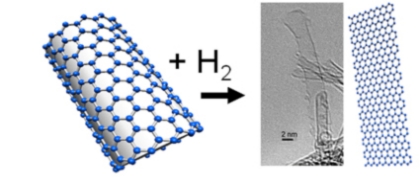
Figure. Researchers unzipped single-walled carbon nanotubes by using a reaction with molecular hydrogen.

In the new study, the research team shows that it is also possible to unzip single-walled carbon nanotubes by using a reaction with molecular hydrogen. Nanoribbons produced by the new method will have hydrogen on Click to Enlargethe edges, which can be an advantage for some applications. Alexandr Talyzin (pictured at left), physicist at Umeå University in Sweden, has over the past decade been studying how hydrogen reacts with fullerenes.

"Treating the carbon nanotubes with hydrogen was a logical extension of our research. Our previous experience has been of great help in this work," says Alexandr Talyzin.

Nanotubes are typically closed by semi-spherical cups, essentially halves of fullerene molecules. The researchers have previously proved that fullerene molecules can be completely destroyed by very strong hydrogenation. Therefore, they expected similar results for nanotube end cups and tried to open the nanotubes via hydrogenation. The effect was confirmed, and additional effects came to light.

Some carbon nanotubes were unzipped into graphene nanoribbons as a result of prolonged hydrogen treatment. Unzipped graphene ribbons with hydrogen attached to the side walls could possibly lead to synthesis of hydrogenated graphene: graphane. So far, graphane synthesis was mostly attempted by reacting hydrogen with graphene. This appeared to be very difficult, especially if the graphene is supported on some substrate and only one side is available for the reaction. However, hydrogen reacts more easily with the curved surface of CNTs.

Ilya V. Anoshkin, Albert G. Nasibulin, Jiang Hua and Esko I. Kauppinen at Aalto University are experts in the synthesis and characterization of singled-walled carbon nanotubes. Valery M. Mikoushkin, Vladimir V. Shnitov and Dmitry E. Marchenko from St. Petersburg made XPS and other characterization using synchrotron radiation. Dag Noréus at Stockholm University shared his expertise with high temperature hydrogen reactors.

The research was published in the journal ACS Nano:
Title: Hydrogenation, Purification, and Unzipping of Carbon Nanotubes by Reaction with Molecular Hydrogen: Road to Graphane Nanoribbons
Authors: Alexandr V. Talyzin, Serhiy Luzan, Ilya V. Anoshkin, Albert G. Nasibulin, Hua Jiang, Esko I. Kauppinen, Valery M. Mikoushkin, Vladimir V. Shnitov, Dmitry E. Marchenko, and Dag Noréus
Access it at http://pubs.acs.org/doi/abs/10.1021/nn201224k

Follow Small Times on Twitter.com by clicking www.twitter.com/smalltimes. Or join our Facebook group