Tag Archives: Small Times Magazine

May 4, 2011 — DelfMEMS, RF MEMS player, has delivered custom samples to telecom operator NTT DOCOMO Inc. DelfMEMS provided arrays of custom micro electromechanical system (MEMS) ohmic switches to enable tunability into radio frequency (RF) frontend modules (FEM) for mobile applications. Voltage, size, losses, isolation, ultra-fast switching time and power handling will be evaluated by NTT DOCOMO according to the 6GHz requested specifications.

DelfMEMS is setting up an open technology platform to propose a new integrated micro-mechanical building block based on a new IP portfolio that solves RF MEMS ohmic switch issues. MEMS switching can reduce power consumption and bill of materials (BOM) by minimizing losses between the antenna and active devices of a FEM.

"We are working on a very basic approach" for RF MEMS, said Olivier Millet, CEO. NTT DOCOMO’s validation of these custom MEMS arrays should increase data transfer and decrease power consumption from handsets to base stations. Current insertion losses of DelfMEMS’ MEMS switches are better than advanced SOI or SoS technologies, added Millet, saying that the company is continually looking to decrease them, lower costs, and shrink sizes.

DelfMEMS develops and markets radio frequency switches based on MEMS technology. Learn more at www.delfmems.com.

Follow Small Times on Twitter.com by clicking www.twitter.com/smalltimes. Or join our Facebook group

May 4, 2011 — A team of researchers at MIT has found a way to manipulate both the thermal and electrical conductivity of materials by changing the external conditions. The technique can change electrical conductivity by factors of well over 100, and heat conductivity by more than threefold.

Researchers used percolated composite materials and manipulated them by controlling their temperature.

Click to Enlarge

Image. An artistic rendering of the suspension as it freezes shows graphite flakes clumping together to form a connected network (dark spiky shapes at center), as they are pushed into place by the crystals that form as the liquid hexadecane surrounding them begins to freeze. SOURCE: Jonathan Tong.

The researchers suspended tiny flakes of one material in a liquid that, like water, forms crystals as it solidifies. For their initial experiments, they used flakes of graphite suspended in liquid hexadecane, but they showed the generality of their process by demonstrating the control of conductivity in other combinations of materials as well. The liquid used in this research has a melting point close to room temperature but the principle should be applicable for high-temperature use as well.

The process works because when the liquid freezes, the pressure of its forming crystal structure pushes the floating particles into closer contact, increasing their electrical and thermal conductance. When it melts, that pressure is relieved and the conductivity goes down. In their experiments, the researchers used a suspension that contained just 0.2% graphite flakes by volume. Particles remain suspended indefinitely in the liquid, as was shown by examining a container of the mixture three months after mixing.

By selecting different fluids and different materials suspended within that liquid, the critical temperature at which the change takes place can be adjusted at will, said Gang Chen, MIT’s Carl Richard Soderberg Professor of Power Engineering and director of the Pappalardo Micro and Nano Engineering Laboratories.

The system that Chen and his colleagues developed could be applied to many different materials for either thermal or electrical applications. One potential use of the new system, Chen explains, is for a fuse to protect electronic circuitry. In that application, the material would conduct electricity with little resistance under normal, room-temperature conditions. But if the circuit begins to heat up, that heat would increase the material’s resistance, until at some threshold temperature it essentially blocks the flow, acting like a blown fuse. Instead of needing to be reset, as the circuit cools down the resistance decreases and the circuit automatically resumes its function. Heat switches exist, but involve separate parts made of different materials, whereas this system has no macroscopic moving parts, says Joseph Heremans, professor of physics and of mechanical and aerospace engineering at Ohio State University.

Another possible application is for storing heat, such as from a solar thermal collector system, later using it to heat water or homes or to generate electricity. The systems much-improved thermal conductivity in the solid state helps it transfer heat.

"Using phase change to control the conductivity of nanocomposites is a very clever idea," says Li Shi, a professor of mechanical engineering at the University of Texas at Austin. MIT is interested in developing other applications for the process now.

Gang Chen, MIT’s Carl Richard Soderberg Professor of Power Engineering and director of the Pappalardo Micro and Nano Engineering Laboratories, is the senior author of a paper describing the process that was published online on April 19 http://www.nature.com/ncomms/journal/v2/n4/full/ncomms1288.html and will appear in a forthcoming issue of Nature Communications. Lead authors are former MIT visiting scholars Ruiting Zheng of Beijing Normal University and Jinwei Gao of South China Normal University, along with current MIT graduate student Jianjian Wang.

The research was partly supported by grants from the National Science Foundation.

Learn more at http://web.mit.edu/

Follow Small Times on Twitter.com by clicking www.twitter.com/smalltimes. Or join our Facebook group

May 3, 2011 — COMSOL Inc., developer of the COMSOL Multiphysics modeling and simulation environment for scientists and engineers, announced that SB Microsystems has achieved COMSOL Certified Consultant status.

SB Microsystems provides engineering expertise in micro electromechanical systems (MEMS) and microfluidic device design, simulation, prototyping, testing, and fabrication. It offers particular expertise in medical and scientific sensors and instrumentation in which micro-scale miniaturization and low power consumption are critical criteria for its clients’ success.

"SB Microsystems enables us to better serve our users developing microfluidic devices as well as those researching and developing new products leveraging MEMS-based technologies in such emerging fields as implantable biological sensors, miniature analytical instruments, and sensors for point-of-care medical testing," said Bernt Nilsson, senior VP of marketing, COMSOL.

SB Microsystems provides research, development, and consulting services for clients both public and private worldwide. The company works with clients at any step within the MEMS and microfluidic device development and fabrication lifecycle. Additional services rendered include process design as well as detailed design ranging from final mask-level layout, circuit design, and CAD drawings of traditionally machined parts. SB Microsystems also maintains in-house testing facilities that can meet requirements ranging from simple acceptance testing through to complete bench-top and environmental characterization.

"Many of our projects begin with theoretical proof-of-concept and continue right on through the formalization of agreements with semiconductor foundries and vendors," says Brian Jamieson, president of SB Microsystems.

A key to SB Microsystems’ attention to good engineering design is its extensive, hands-on experience with such state-of-the-art techniques and tools as the COMSOL MEMS Module, according to Jamieson. The module, which solves problems that couple structural mechanics, microfluidics, and electromagnetics, extends the core capabilities of the COMSOL Multiphysics modeling and simulation environment for the unique engineering problems encountered in the design and modeling of microscale electro-mechanical systems.

COMSOL’s flagship product is COMSOL Multiphysics, a software environment for the modeling and simulation of any physics-based system. A particular strength of COMSOL Multiphysics is its ability to account for multiple physics phenomena simultaneously. Optional modules add discipline-specific tools for acoustics, batteries and fuel cells, chemical engineering, electrodeposition, electromagnetics, fluid dynamics, geomechanics, heat transfer, MEMS, plasma, structural analysis, and subsurface flow.

The COMSOL MEMS Module enables SB Microsystems to address almost all simulations in the microscale domain. "As a COMSOL Certified Consultant," says Jamieson, "we are able to offer manufacturers and developers of highly miniaturized sensors and instruments certified expertise in the modeling and simulation of the coupled mechanical, thermal, and electrical phenomena inherent in MEMS and micro-fluidic devices."

COMSOL Certified Consultants produce ready-to-run models and reports as well as in-depth analyses of simulation results. The collective expertise of the COMSOL Certified Consultant group covers a breadth of applications and has resulted in the commercialization of many patented products. For further information about COMSOL Certified Consultants, visit www.comsol.com/company/consultants.

SB Microsystems helps its clients develop highly miniaturized medical and scientific sensors and systems using modern micro-fabrication technologies such as MEMS. To contact SB Microsystems for further information, visit www.sbmicrosystems.us.

Follow Small Times on Twitter.com by clicking www.twitter.com/smalltimes. Or join our Facebook group

May 3, GLOBE NEWSWIRE — FEI Company (Nasdaq:FEIC), instrumentation company, is extending its ChemiSTEM Technology to enable atomic-level energy dispersive X-ray (EDX) spectroscopy across the periodic table.

The combination of increased current in an atomic-sized probe by Cs-correction and the increase in X-ray detection sensitivity and beam current of the ChemiSTEM Technology allows results to be obtained within minutes.

Figures. Atomic-level EDX spectroscopy of the material Strontium Titanate; the individual atomic positions of the crystal structure can be easily distinguished by their chemical signal (red is Strontium, green is Titanium). These images are based on raw data, with no signal post-processing, and the individual atomic column positions in the structure are visible and clearly distinguished from their neighbors with very high contrast and signal-to-noise quality. The sampling of these atomic-level chemical maps is 0.075 Angstroms per pixel, the highest sampling density obtained so far by any atomic spectroscopy technique using scanning/transmission electron microscopy (S/TEM). These chemical maps were acquired in just minutes on a Titan G2 60-300 S/TEM with ChemiSTEM Technology.

"One of the most important applications for the new technology will be element-specific imaging at atomic resolution," said Professor Ferdinand Hofer of Graz University of Technology, Austria. The technology will be applied to study interfaces in semiconductors, solar cell materials, LEDs and ceramic materials with previously unknown detection sensitivity and accuracy.

George Scholes, FEI’s vice president for product management, adds, "The ChemiSTEM Technology will enable breakthough results in many key application areas for our customers, such as catalysis, metallurgy, microelectronics, and green energy materials, to name a few. For example, in a recent experiment with ChemiSTEM Technology, our customer was able to clearly resolve the core-shell structure of 5nm catalyst nanoparticles in about three minutes and with three times greater pixel resolution than a previous experiment with conventional technology. And the conventional technology failed after three hours of data collection to clearly resolve the same structure."

ChemiSTEM Technology achieves a factor of 50 or more enhancement in speed of EDX elemental mapping on scanning/transmission electron microscopes (S/TEMs) compared to conventional technology employing standard EDX Silicon-drift detectors (SDDs) and standard Schottky-FEG electron sources. It combines FEI’s proprietary X-FEG high brightness electron source, providing up to five times more beam current at a given spatial resolution; the patent-pending Super-X detection system, providing up to ten times or more detection sensitivity in EDX; and fast scanning electronics, capable of achieving EDX spectral rates of up to 100,000 spectra per second. Additionally, the windowless detector design employed for each of ChemiSTEM Technology’s four integrated SDD detectors has proven to optimize the detection of both light and heavy elements.

This combination of high detection sensitivity and high spectral rates of up to 100,000 spectra per second are enabling better EDX mapping of materials that are highly sensitive to electron beam damage, such as composition analysis in nanometer-scale Indium Gallium Nitride quantum wells used in light emitting diode (LED) devices, and semiconductor devices with potentially mobile dopant materials, as well as many others devices used in emerging nanotechnologies.

FEI (Nasdaq:FEIC) provides electron- and ion-beam microscopes and tools for nanoscale applications across many industries: industrial and academic materials research, life sciences, semiconductors, data storage, natural resources and more. More information can be found at www.fei.com.

Follow Small Times on Twitter.com by clicking www.twitter.com/smalltimes. Or join our Facebook group

May 3, 2011 — Solid State System Co., Ltd (3S), an IC design house, released engineering samples of its wafer-level micro electromechanical system (MEMS) microphone. SSSM100 is a tiny analog output CMOS MEMS microphone manufactured under standard CMOS process and wafer level packaging (WLP) technology.

Differing from most of the other MEMS microphones that need separate chips, SSSM100 has successfully integrated the MEMS sensor and the amplifier onto one single chip. 3S expects the resulting small form factor to give users flexibility in design. Engineering samples are available.

Solid State System Co., Ltd (3S) provides IC design and related test equipment for Flash Data Storage Controller ICs, Multi-media ICs, as well as a line of non-volatile Memory ASICs, and now MEMS. Learn more at www.3system.com.tw

Follow Small Times on Twitter.com by clicking www.twitter.com/smalltimes. Or join our Facebook group

May 3, 2011 — Camtek Ltd. (NASDAQ and TASE: CAMT) received a follow-on order for its new Gannet automatic optical inspection (AOI) system for the front-end semiconductor industry.

The order is a repeat order for two systems from a leading Asian integrated device manufacturer (IDM), previously supplied with multiple Gannet systems. The systems are expected to be installed during the second quarter of 2011.

This order is for the application of CMOS image sensor inspection, using Camtek’s latest technology with advanced detection capabilities developed for the front-end semiconductor market. Camtek’s Gannet system offers a combination of exceptional detection solutions for a variety of processes, high productivity, and supports tight process control for high-volume manufacturing. 

Camtek Ltd provides automated solutions dedicated for enhancing production processes and yield, enabling our customers new technologies in semiconductors, and PCB and IC substrates.

Camtek addresses the specific needs of these industries with dedicated solutions based on a wide and advanced platform of technologies including intelligent imaging, image processing, ion milling and digital material deposition. Learn more at www.camtek.co.il.

May 2, 2011 – Marketwire — Robert Bosch GmbH (Bosch), one of the top 4 MEMS suppliers, has standardized on an enhanced custom/analog flow based on Virtuoso v6.1 technology from Cadence Design Systems Inc. (NASDAQ: CDNS), gaining approximately 25% better productivity for advanced custom/analog silicon design.

Bosch and Cadence continue to build upon their longstanding collaboration with the aim of accelerating Bosch’s innovation and time to market, while ensuring the highest quality and reliability for its broad range of high-performance integrated circuits (ICs). The Cadence custom/analog flow includes all elements of silicon, package, and board and provides unified design intent, abstraction, and convergence through the flow.

As a result of implementing the Cadence unified custom/analog flow, Bosch yielded approximately a 25% design productivity gain compared to a multi-vendor point-tool approach that was used in previous designs. Significant productivity and quality gains were achieved by leveraging the constraint-driven design methodology and the new electrically driven design framework in the latest version of the Cadence Virtuoso v6.1 custom IC design technology.

Driving design intent and convergence pervasively through the custom/analog flow is especially critical for the high-performance and strict reliability requirements of the automotive IC industry. The Cadence unified custom/analog flow provides Bosch an integrated and modular IC development flow well suited for modern IC and micro electro mechanical system (MEMS) technologies.

Leveraging a holistic constraint-driven design methodology across a common backplane through Cadence Virtuoso Schematic Editor, Virtuoso Analog Design Environment, and Virtuoso Layout Suite, Bosch was able to save design time across all process technologies and meet the high quality standards for its safety-critical applications.

"Serving a very cost-sensitive market such as automotive with high-quality standards requires a comprehensive design, verification, and implementation solution which is based on a proven design methodology within a powerful automated design environment," said Dr. Peter van Staa, VP engineering at Bosch.

"Being selected by Bosch, the leading worldwide supplier for automotive electronics, underscores the significant technology leadership Cadence offers to advanced custom/analog design teams," said John Stabenow, group director, custom/analog product management at Cadence. "We are committed to the EDA360 vision and delivering on the promise of a more deterministic end-to-end path to silicon, as well as the industry call for higher productivity and profitability."

The enhanced custom/analog flow is focused on unique and pervasive design intent, abstraction, and convergence from schematic-to-GDSII, through to packaging.

Cadence enables global electronic design innovation and plays an essential role in the creation of today’s integrated circuits and electronics. More information about the company, its products, and services is available at www.cadence.com.

Follow Small Times on Twitter.com by clicking www.twitter.com/smalltimes. Or join our Facebook group

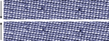
May 2, 2011 — Asylum Research’s Cypher atomic force microscope (AFM) is routinely achieving resolution of atomic-scale point defects in liquid.  While scanning tunneling microscopes have demonstrated point defect resolution since their invention, it has been more elusive in AFM.  Many commercial AFMs can routinely image atomic lattices in ambient and liquid conditions, but the lack of point defects has led most researchers to conclude that the contact areas are typically several atoms across. 

Click to Enlarge

Figure. Successive AC mode topography images of the cleavage plane of a calcite crystal in water. The repeated point defects demonstrate the true atomic resolution capabilities of the Cypher AFM.  Arrows indicate scan direction.  Scan size 20nm; Z scale 3.2Å; Cantilever Amplitude 4Å; Cantilever Frequency 454 kHz.

More recently, instrumental improvements have brought true atomic resolution to ultra-high vacuum (UHV) AFM.  Achieving true-atomic resolution under ambient conditions at the liquid-solid interface brings this resolution to an environment highly relevant for much practical research.  The Cypher AFM’s signal-to-noise and support for ultra-small probes have enabled this breakthrough in atomic scale imaging.

Asylum Research took the most popular imaging mode, AC-mode (also known as tapping, intermittent-contact, or dynamic AFM) and improved the resolution, Jason Cleveland, Asylum Research CEO, said. It was achieved with improved signal-to-noise ratio from the use of ultra-small cantilevers with megahertz resonant frequencies in liquid; the optical lever detection noise floor was pushed to 25 fm/rtHz, allowing the measurements to remain thermally limited even with very stiff cantilevers and amplitudes as small as 1 Angstrom. Cypher’s low open-loop noise of 5pm in X, Y, and Z allows the stability to image at this scale, even on a scanner with a 30µm lateral range.

Asylum Research provides atomic force and scanning probe microscopy (AFM/SPM) for materials and bioscience applications. Asylum’s Cypher AFM is a small sample AFM/SPM providing low-drift closed loop atomic resolution. Learn more at www.AsylumResearch.com.

Follow Small Times on Twitter.com by clicking www.twitter.com/smalltimes. Or join our Facebook group

May 2, 2011 — US Department of Energy (DOE) Brookhaven National Laboratory researchers are using precise atom-by-atom molecular beam epitaxy (MBE) layering to fabricate an ultrathin transistor-like field effect (FET) device to study the conditions that turn insulating materials into high-temperature superconductors. This advances our understanding of high-temperature superconductivity, and could also accelerate the development of resistance-free electronic devices.
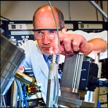
Click to Enlarge"Understanding exactly what happens when a normally insulating copper-oxide material transitions from the insulating to the superconducting state is one of the great mysteries of modern physics," said Brookhaven physicist Ivan Bozovic, lead author on the study and pictured here.

One way to explore the transition is to apply an external electric field to increase or decrease the level of doping (the concentration of mobile electrons in the material) and see how this affects the ability of the material to carry current. But to do this in copper-oxide (cuprate) superconductors, one needs extremely thin films of perfectly uniform composition and electric fields measuring more than 10 billion volts per meter.

Bozovic’s group used molecular beam epitaxy to uniquely create such perfect superconducting thin films one atomic layer at a time, with precise control of each layer’s thickness. They’ve shown that in such MBE-created films even a single cuprate layer can exhibit undiminished high-temperature superconductivity.

Now, they’ve applied the same technique to build ultrathin superconducting field effect devices that allow them to achieve the charge separation, and thus electric field strength, for these critical studies.

These devices are similar to field-effect transistors (FETs), in which a semiconducting material transports electrical current from the source electrode on one end of the device to a drain electrode on the other end. FETs are controlled by a third electrode, the gate electrode, positioned above the source-drain channel.

No known insulator could withstand the high fields required to induce superconductivity in the cuprates. This renders the standard FET scheme impossible for high-temperature superconductor FETs. Instead, the scientists used electrolytes, liquids that conduct electricity, to separate the charges. When an external voltage is applied, the electrolyte’s positively charged ions travel to the negative electrode and the negatively charged ions travel to the positive electrode. But when the ions reach the electrodes, they abruptly stop. The electrode walls carry an equal amount of opposite charge, and the electric field between these two oppositely charged layers can exceed the 10 billion volts per meter goal.

The result is a field effect device in which the critical temperature of a prototype high-temperature superconductor compound (lanthanum-strontium-copper-oxide) can be tuned by as much as 30 degrees Kelvin, which is about 80% of its maximal value — almost ten times more than the previous record.

The scientists have now used this enhanced device to study some of the basic physics of high-temperature superconductivity. As the density of mobile charge carriers is increased, their cuprate film transitions from insulating to superconducting behavior when the film sheet resistance reaches 6.45 kilo-ohm. This is exactly equal to the Planck quantum constant divided by twice the electron charge squared — h/(2e)2. Both the Planck constant and electron charge are atomic units.

"It is striking to see a signature of such clearly quantum-mechanical behavior in a macroscopic sample (up to millimeter scale) and at a relatively high temperature," Bozovic said.

The findings imply that electrons form pairs (although localized and immobile) in the insulating state, as well as the superconducting state, unlike in any other known material. That sets the scientists on a more focused search for what gets these immobilized pairs moving when the transition to superconductivity occurs.

Superconducting FETs might also have direct practical applications. Semiconductor-based FETs are power-hungry, particularly when packed very densely to increase their speed. In contrast, superconductors operate with no resistance or energy loss. Here, the atomically thin layer construction enhances the ability to control superconductivity using an external electric field.

The technical breakthrough is described in the April 28, 2011, issue of Nature (http://www.nature.com/nature/journal/v472/n7344/full/nature09998.html). Coauthors on the paper include: I. Bozovic, A. Bollinger, J. Yoon, and J. Misewich from Brookhaven Lab and G. Dubuis and D. Pavuna from Ecole Polytechnique Federale de Lausanne (Switzerland).

This research was funded by the DOE Office of Science and the Swiss National Science Foundation.

Follow Small Times on Twitter.com by clicking www.twitter.com/smalltimes. Or join our Facebook group

April 29, 2011 — Magnetics researchers at the National Institute of Standards and Technology (NIST) created "eggcentric" nanomagnets, suggesting strategies for making future low-power computer memories.

Click to Enlarge

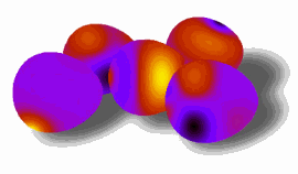
NIST researchers used electron-beam lithography (e-beam lithography) to make thousands of nickel-iron magnets, each about 200nm in diameter. Each magnet is ordinarily shaped like an ellipse, a slightly flattened circle. Researchers also made some magnets in three different egglike shapes with an increasingly pointy end. It’s all part of NIST research on nanoscale magnetic materials, devices and measurement methods to support development of future magnetic data storage systems.

Even small distortions in magnet shape can lead to significant changes in magnetic properties. Researchers discovered this by probing the magnets with a laser and analyzing what happens to the electron spins. Changes in the spin orientation can propagate through the magnet like waves at different frequencies. The more egg-like the magnet, the more complex the wave patterns and their related frequencies.  The shifts are most pronounced at the ends of the magnets.

To confirm localized magnetic effects and "color" the eggs, scientists made simulations of various magnets using NIST’s object-oriented micromagnetic framework (OOMMF). Lighter colors indicate stronger frequency signals.

The egg effects explain erratic behavior observed in large arrays of nanomagnets, which may be imperfectly shaped by the lithography process. Such distortions can affect switching in magnetic devices. The egg study results may be useful in developing random-access memories (RAM) based on interactions between electron spins and magnetized surfaces. Spin-RAM is one approach to making future memories that could provide high-speed access to data while reducing processor power needs by storing data permanently in ever-smaller devices. Shaping magnets like eggs breaks up a symmetric frequency pattern found in ellipse structures and thus offers an opportunity to customize and control the switching process.

"Intentional patterning of egg-like distortions into spinRAM memory elements may facilitate more reliable switching," says NIST physicist Tom Silva, who co-authored the paper on this work: H.T. Nembach, J.M. Shaw, T.J. Silva, W.L. Johnson, S.A. Kim, R.D. McMichael and P. Kabos. Effects of shape distortions and imperfections on mode frequencies and collective linewidths in nanomagnets. Physical Review B 83, 094427, March 28, 2011.

The National Institute of Standards and Technology (NIST) is an agency of the U.S. Commerce Department. Learn more at www.nist.gov

Follow Small Times on Twitter.com by clicking www.twitter.com/smalltimes. Or join our Facebook group