Tag Archives: Small Times Magazine

April 13, 2011 — Dolomite, microfluidic designer and manufacturer, launched a range of optical systems that capture high-quality still and moving images of microfluidic experiments.

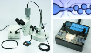
Click to EnlargeThe range of optical systems includes a high-speed camera and microscope system, providing a flexible solution for general microscopy including droplet generation and particle imaging. The system’s microscope offers zoom ratio of 7.5:1 and good working distance for a range of samples. The camera integrates with the microscope to capture images at over 1000 frames per second. The universal stand enables flexible microscope positioning.

The microscope stage is designed to accommodate all types of microfluidic chips and enables users to quickly locate and observe the area of interest. It can, for example, be used in conjunction with Dolomite’s Droplet Junction Chips for the improved visibility of droplet formation: droplet monodispersity, rate of production, and stability. The stage also features a 150W halogen cold light source with continuous dimming and no flicker effect at short exposure times.

Dolomite’s also offers a digital microscope that can be connected to a PC using a USB cable. The product is compact and low-cost for general microscopy, and Dolomite claims that it outweighs many of the USB microscopes currently available in image quality.

For further information on Dolomite’s range of Optical Systems as well as the complete portfolio of microfluidic products including chips, connectors/ interconnects, pumps, valves and custom devices, visit www.dolomitemicrofluidics.com.

Follow Small Times on Twitter.com by clicking www.twitter.com/smalltimes. Or join our Facebook group
April 13, 2011 — In a paper published March 29 in the Proceedings of the National Academy of Sciences, Qiaoqiang Gan, PhD, an assistant professor of electrical engineering at the University at Buffalo’s (UB’s) School of Engineering and Applied Sciences, and his colleagues at Lehigh University, where he was a graduate student, described how they slowed broadband light waves using a type of material called nanoplasmonic structures.

The goal is to create multiplexed, multiwavelength communications, where optical data can potentially be tamed at different wavelengths, increasing processing and transmission capacity.

Gan notes that if light could ever be stopped entirely, new possibilities would open up for data storage.

"At the moment, processing data with optical signals is limited by how quickly the signal can be interpreted," he says. "If the signal can be slowed, more information could be processed without overloading the system."

Gan and his colleagues created nanoplasmonic structures by making nanoscale grooves in metallic surfaces at different depths, which alters the materials’ optical properties.

These plasmonic chips provide the critical connection between nanoelectronics and photonics, allowing these devices to be integrated for optical computing, "lab-on-a-chip" biosensors and more efficient, thin-film photovoltaic materials.

The optical properties of the nanoplasmonic structures allow different wavelengths of light to be trapped at different positions in the structure, potentially allowing for optical data storage and enhanced nonlinear optics. Conventional methods can only trap a single wavelength in a narrow band.

"Light is usually very fast, but the structures I created can slow broadband light significantly," says Gan, thanks to the structures’ engineered surface "plasmon resonances," where light excites the waves of electrons that oscillate back and forth on metal surfaces.

In this case, he says, light can be slowed down and trapped in the vicinity of resonances in this novel, dispersive structural material.

Gan and his colleagues also found that because the nanoplasmonic structures they developed can trap very slow resonances of light, they can do so at room temperature, instead of at the ultracold temperatures that are required in conventional slow-light technologies.

"In the PNAS paper, we showed that we trapped red to green," explains Gan. "Now we are working on trapping a broader wavelength, from red to blue. We want to trap the entire rainbow."

Gan, who was hired at UB under the UB 2020 strategic strength in Integrated Nanostructured Systems, will be working toward that goal, using the ultrafast light source in UB’s Department of Electrical Engineering in the laboratory of UB professor and vice president for research Alexander N. Cartwright.

"This ultrafast light source will allow us to measure experimentally just how slow is the light that we have trapped in our nanoplasmonic structures," Gan explains. "Once we know that, we will be able to demonstrate our capability to manipulate light through experiments and optimize the structure to slow the light further."

Co-authors with Gan on the study are Filbert Bertoli, Yongkang Gao, Yujie Ding, Kyle Wagner and Dmitri Vezenov, all of Lehigh University.

Follow Small Times on Twitter.com by clicking www.twitter.com/smalltimes. Or join our Facebook group

April 12, 2011 — After unprecedented 2010 increases, total optoelectronics, sensors, and discretes (O-S-D) revenues are predicted to hit $58.3 billion in 2011, says IC Insights.

Slightly above average growth rates in 2011 will lift sales of optoelectronics, sensors and actuators, and discrete semiconductors to new record-high levels again this year following unprecedented increases in the 2010 recovery year, according to IC Insights’ newly completed 2011 Optoelectronics, Sensors, and Discretes (O-S-D) Report.

The optoelectronics market will grow 11% to $26.4 billion in 2011; sensor/actuator sales will increase 15% to $8.5 billion; and discretes dollar volume will rise 8% to $23.4 billion this year, according to the report’s data. Sales growth in these three semiconductor market segments is being driven by strong demand for accelerometers and gyroscope sensors built with microelectromechanical systems (MEMS) technology, high-brightness light-emitting diodes (LEDs), optical-network laser transmitters, CMOS image sensors, and power transistors.

Click to Enlarge

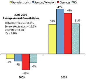
Figure. Sales changes in the economic downturn and recovery. SOURCE: IC Insights

In the strong 2010 semiconductor recovery from the 2009 downturn year, the optoelectronic, sensor/actuator, and discrete markets racked up impressive gains with combined O-S-D revenues rising 37% to a record-high total of $52.9 billion (Figure). The 2010 increase was the highest annual growth ever recorded for total O-S-D sales.

Due to a relatively weak recovery in image sensors, 2010 optoelectronics sales grew just 30% to $23.9 billion, which was the fifth largest increase for this market in three decades.

Sensors/actuators sales surged 45% in 2010 to $7.4 billion, which was the greatest increase ever for this industry category.

Discretes revenues climbed 42% to $21.6 billion, which was the highest percentage growth for this commodity-filled semiconductor market since the 1970s.

While much of the 2010 increase in O-S-D sales was driven by the economic recovery and the need to refill depleted inventories, substantial real market growth occurred last year — going beyond just making up for lost growth in the downturn. When the combined effects of the 2009 slump and 2010 recovery are added together, all three O-S-D market segments exceeded their normal annual average growth rates in the two-year period (see figure). All three segments also reached new annual sales records in 2010.

The new O-S-D Report shows seven product categories setting new sales records in 2010: lamp devices (i.e., LEDs); optocouplers and switches; pressure sensors; acceleration/yaw sensors; magnetic-field sensors; power transistors; and rectifiers.

Total sales for all MEMS-based sensors and actuators also climbed 47% to a new record-high $6.2 billion in 2010. In addition to new all-time peaks being set again in these seven product categories and MEMS-based devices in 2011, IC Insights is forecasting new sales records being reached in total image sensors, CMOS image sensors, actuators, and diodes.

Learn more about the report by emailing Rob Lineback at [email protected]

Follow Small Times on Twitter.com by clicking www.twitter.com/smalltimes. Or join our Facebook group

April 12, 2011 — The MEMS industry grew 25% in 2010, and the 4 largest companies grew even faster, increasing their domination of Yole Développement’s annual top 30 MEMS company ranking. These giants now account for some $2.9 billion of the sector’s $8.6 billion in total sales.

MEMS may still be an industry with a multitude of diverse products, but it’s also increasingly an industry dominated by a limited number of big suppliers.

Figure. Top 30 worldwide MEMS companies ranking – 2010 revenues estimates ($M). SOURCE: Yole Développement April 2011.

Blockbuster recovery and inventory restocking from the automotive sector, and the rush to put inertial sensors in every handheld device, drove a healthy 25% jump in total MEMS sales in 2010, to some $8.6 billion. But it particularly meant a boom year for high-volume MEMS suppliers to big customers. The big four — Texas Instruments, Hewlett Packard, Robert Bosch, and STMicroelectronics — increased their combined MEMS sales by some 37%, to ~$2.9 billion, as they aggressively ramped volumes and shrank die size to drive down costs, and widened the gap with their smaller challengers. Sales of the big four now account for about one third of total MEMS industry revenues.

IHS iSuppli’s Jérémie Bouchaud estimates:

  • STMicroelectronics N.V. (STM) revenue for MEMS sensors (not counting its foundry work for inkjet printers) exceeded $353 million in 2010, up 63% from $216 million in 2009.
  • The Bosch Group GmbH reached $643 million in MEMS revenue in 2010, up 46% from $440 million in 2009.
  • VTI Technologies Oy reached $100 million in 2010, up 35% from $75 million in 2009.
  • TI enjoyed nearly 25% growth in 2010, third best among the top-10, raking in $793M worth of MEMS. Also read: European MEMS top dogs led the pack in 2010 and Texas Instruments regains MEMS leadership in 2010, thanks to DLP chips

"It’s very important to be big to succeed in the consumer and automotive markets," says Jean Christophe Eloy, CEO of Yole Developpement. A company needs to be able to ramp volume on 8" wafers to reduce costs, and to continue to invest in shrinking the die to drive ASP down, Eloy adds. Companies with smaller size will remain flat or will get pushed out. Yole sees 3 groups of MEMS companies, those with sales above $500M (the leaders, involved in consumer electronics and/or automotive businesses), those with sales between $500M and $200M (the companies that still can become global leaders in MEMS), and those below $200M (companies that have to specialize in specific businesses in order to be profitable)."

There’s plenty of industry-leading growth among the rest of the top 30 companies as well. This year, it took sales of $52 million to make the ranking, up from $31 million last year. Five additional players reached $100 million+ in MEMS sales, bringing 21 of the 30 to a level likely needed to stay competitive in the consumer or automotive business. The top 30 companies now account for about 80% of total MEMS industry sales.

Yole Développement defines micro electro mechanical systems (MEMS) for this listing as three-dimensional structures made by semiconductor processes, with primarily physical or mechanical function. This year, magnetic sensors were also included because they are becoming so closely integrated with MEMS inertial sensors.

Yole Développement’s 8 MEMS analysts base this annual listing both on direct discussions with the companies in their particular fields as they track some 150-200 MEMS companies throughout the year, and also cross checked with their bottom-up analysis of MEMS device markets. For more information, visit www.i-micronews.com.

Follow Small Times on Twitter.com by clicking www.twitter.com/smalltimes. Or join our Facebook group

April 11, 2011 – Marketwire — NanoProfessor, a division of NanoInk Inc. focused on nanotechnology education, implemented its NanoProfessor Nanoscience Education Program at the University of Calgary in Alberta, Canada. The school is the first in Canada to use this nano education program.

The University of Calgary’s Nanoscience program provides a working knowledge of nanotechnology and exposure to cutting-edge instrumentation used to fabricate nanomaterials. The NanoProfessor Program helps the University of Calgary meet this objective by providing instrumentation, curriculum, and hands-on labs to expand students’ understanding, skills, and real-world experience needed to succeed in the growing nanotechnology industry.

"We are committed to providing our students with a meaningful education based on the principle of learning science by doing science," said David Cramb, Director of the Nanoscience program at the University of Calgary. "Not only does the NanoProfessor Program enhance our ability to provide students with a practical learning experience, but NanoInk’s NLP 2000 Desktop Nanofabrication System allows us to expand our research capability through the versatility of Dip Pen Nanolithography (DPN)."

The NanoProfessor Nanoscience Education Program will complement the University of Calgary’s existing nanoscience educational offerings, covering medicine, materials, energy, electronics, biotechnology and more.

The NanoProfessor Nanoscience Education Program aims to expand hands-on nanotechnology education from the cleanrooms of research-based universities to undergraduate classrooms, and suits nanotechnology educational initiatives at the community college, technical institute, and undergraduate university level. The program alternates between classroom lectures and hands-on lab work and includes a textbook authored by leading nanotechnology experts, covering the topics of Nanotechnology Basics, NanoPhysics, NanoChemistry, NanoBiology and Environmental, Health, and Safety perspectives on nanotechnology.

During the hands-on lab experiments, students learn the fundamentals for building custom-engineered, nanoscale structures while working with state-of-the-art equipment including NanoInk’s NLP 2000 Desktop NanoFabrication System, a student-friendly atomic force microscope (AFM), an advanced fluorescence microscope, and various chemical and biological materials used in current and emerging nanotechnology applications.

The NanoProfessor Nanoscience Education Program aims to advance the field of nanoscience and address the growing need for a skilled workforce of nanotechnologists. Learn more at www.NanoProfessor.net.

The University of Calgary is a comprehensive research university, ranked one of Canada’s top seven research universities and a member of the 13 most research intensive universities in Canada, combining the best of long-established university traditions with the city of Calgary’s vibrant energy and diversity. More information is available at http://ucalgary.ca/

Follow Small Times on Twitter.com by clicking www.twitter.com/smalltimes. Or join our Facebook group

April 11, 2011 – FARS News Agency — A group of Iranian researchers from Isfahan University of Technology, in cooperation with colleagues at Italy’s University of Palermo, synthesized titanium oxide nanotubes.

Titanium oxide nanotubes are semiconductors with a parallel and regular structure. They also have a high optical and chemical stability, and they are widely used in the photo-electrochemical decomposition of water, production of dye sensitized solar cells, and hydrogen sensors.

"We carried out a number of research works to study the structure and electrochemical and photo-electrochemical properties of titanium oxide nanotubes, so that we can use such materials in various applications," Dr Seyed Shahab Miraqayee, one of the researchers of the plan, told INIC. "First, we produced titanium oxide nanotubes in organic and aqueous solutions containing fluorine ion through the anodization of pure titanium plate in a constant electrical potential. Then, we carried out another anodization process in order to stabilize the interface between metal and oxide and also to study the reasons for and the effects of the formation of a blocking layer during the anodization."

According to Miraqayee, the main result of the research is that the synthesized nanotubes do not stick to the surface of the sub-layer titanium metal through an electrochemical and photo-electrochemical method. "Titanium oxide nanotubes have many applications in the production of renewable energies and in the reduction of pollution," he concluded.

Copyright 2011 Fars News Agency.

Follow Small Times on Twitter.com by clicking www.twitter.com/smalltimes. Or join our Facebook group

April 11, 2011 — Movea, motion technology developer, created a wireless, miniaturized, inertial measurement unit (IMU) that uses MEMS sensors to accurately measure 9 degree-of-freedom (DOF) motion with a PCB module that is about the size of a small wristwatch.

The MotionPod is a patented hardware solution for motion sensing that incorporates a 3-axis accelerometer, a 3-axis gyroscope and a 3-axis magnetometer in fully integrated package complete with software and wireless interface. The miniaturized MotionPod is now an off-the-shelf component, ready to be used in fitness, gaming, and sports applications.

It is also successfully being used by RM Ingénierie, a subsidiary of the CEGEDIM Group, to enable a new generation of joint assessment and rehabilitation applications. Sam Guilaumé, Movea’s CEO, notes that the nine-axis sensing device provides "precise, real-time angular information with a dynamic accuracy of 1 degree, enabling very accurate measurement of rehabilitation and fitness activities." The MotionPods capture limb movement and provide precise information on limb orientation and mobility. MotionPods provide a fast and accurate record of a patient’s progress to be used for biofeedback into evaluation and exercises, making limb rehabilitation interesting and fun by engaging the patient.

A single MotionPod can provide information like range of motion, rotation, speed, and acceleration. Multiple MotionPods can also be networked to gather information simultaneously from different parts of the body for applications such as performance analysis and full body motion capture. The MotionPod measures 33 x 22 x 15mm (1.3 x 0.8 x 0.6") and weighs 14g (0.5 oz). It is designed to clip onto a strap for easy attachment to the body or even to be patched directly onto the body.

Each MotionPod has a built-in, 2.4GHz wireless transmitter that uses Movea’s proprietary wireless technology to deliver a range of up to 30m (100ft) with very low power consumption to maximize battery life, providing up to 8 hours of usage. Data from the MotionPod is transmitted wireless to a receiver connected to a computer via a standard USB connection. Up to 32 MotionPods can be connected to a single MotionController.

The MotionPod comes with Movea’s SmartMotion Development Kit (SMDK) which provides a Windows-based API allowing application developers, systems integrators and OEMs to rapidly integrate and customize the use of wireless multi-sensors in their applications. It also includes a companion application, the MotionDevTool that has an intuitive graphical user interface (GUI) for real-time visualization and integration.

Movea is a leading provider of motion processing chips, software, firmware, and IP for the consumer electronics industry. Further information about Movea can be found at www.movea.com.

Follow Small Times on Twitter.com by clicking www.twitter.com/smalltimes. Or join our Facebook group

April 8, 2011 — The "Printed, Organic & Flexible Electronics Forecasts, Players & Opportunities 2011-2021" report from IDTechEX provides detailed ten year forecasts by device type and analysis by territory, printed vs non printed, rigid vs flexible, inorganic vs organic, cost of materials vs process cost and more.

IDTechEx find that the market for printed and thin film electronics will be $2.2 billion in 2011. 43% of that will be predominately organic electronics, such as OLED display modules. Of the total market in 2011, 38% will be printed. Initially photovoltaics, OLED and e-paper displays grow rapidly, followed by thin film transistor circuits, sensors and batteries. By 2021 the market will be worth $44.25 billion, with 56% printed and 43% on flexible substrates.

The report summarizes activities of over 1000 leading companies. The report addresses all thin film photovoltaics, relevant display technologies, and electronics that will be printed, organic and/or flexible in the future. Realistic timescales, case studies, existing products and the emergence of new products are given, as are impediments and opportunities for the years to come.

Over 3,000 organizations are pursuing printed, organic, flexible electronics, including printing, electronics, materials and packaging companies. While some of these technologies are in use now, with substantial growth in thin film photovoltaics for example, others such as thin film transistors, developed by over 500 organizations, are only just becoming commercially available.

However, the topic is even bigger than this with some conventional electronics such as conventional aSi Photovoltaics now migrating to being printed, to reduce cost, be available on flexible substrates and in larger areas. In addition to the above, forecasts for such markets are given, as is progress to print them. 

Benefits include lower cost, improved performance, flexibility, transparency, reliability, better environmental credentials, and more. Many of the applications will be newly created, and where existing electronic and electrical products are impacted, the extent will be varied. This widely referenced IDTechEx report brings it all together, with particular focus on applications and quantative assessment of opportunities.  

The report covers case studies of where printed electronics are used, why, and the results. It looks at new products that are emerging and their prospects for success. The technical barriers and commercial barriers are listed and prioritized, as well as progress to overcome these. Ten year forecasts are given, along with companies and their activities, case studies, impediments to commercialization and timescales, for: 

  • Logic and memory
  • OLED displays
  • OLED lighting
  • Electrophoretic displays
  • Electrochromic displays
  • Electroluminescent displays
  • Other displays
  • Batteries
  • Photovoltaics
  • Sensors
  • Conductors
  • Other

Access the report at http://www.idtechex.com/research/reports/printed-organic-and-flexible-electronics-forecasts-players-and-opportunities-2011-2021-000264.asp

Follow Small Times on Twitter.com by clicking www.twitter.com/smalltimes. Or join our Facebook group

April 7, 2011 — ST Microelectronics (NY: STM, STMicro) has installed a µPG101 from Heidelberg Instruments in the "More Than Moore" Research Labs in Agrate Brianza (Italy) to develop prototypes of new microfluidics devices for medical diagnostic, and lab-on-chip applications.

The µPG101 is an economical and easy to use Micro Pattern Generator for direct write applications as well as low-volume mask making. It can be used in rapid prototyping of 2D and 3D microstructures on substrates up to 4 by 4", and is capable of exposing high resolution designs with minimum features of 1µm and an address grid of 40nm.

STMicroelectronics supplies semiconductors for the industrial market, set-top box applications, and micro-electromechanical systems (MEMS) chips for portable and consumer devices, including game controllers and smart phones. ST’s process technology portfolio includes advanced CMOS (Complementary Metal Oxide Semiconductor) logic including embedded memory variants, mixed-signal, analog and power processes.

Heidelberg Instruments produces high-precision maskless lithography systems for direct writing and photomask production in the areas of MEMS, BioMEMS, Nano Technology, ASICS, TFT, Plasma Displays, Micro Optics, and many other related applications.

Follow Small Times on Twitter.com by clicking www.twitter.com/smalltimes. Or join our Facebook group

April 7, 2011 — Agilent Technologies Inc. (NYSE: A) released Agilent NanoSuite 6.0, an enhanced-performance software package designed for use with Agilent Nano Indenter G200, G300 and T150 UTM systems. NanoSuite 6.0 promises speed, flexibility, ease of use and new application methods for nanomechanical properties measurements involving polymers, composites, thin film materials, MEMS, surface topology, stiffness mapping, and scratch testing.

NanoSuite 6.0 builds upon the intuitive interface, versatile imaging capabilities, survey scanning, and streamlined test-method development features introduced in the package’s previous iteration. The NanoSuite 6.0 software package offers several groundbreaking test methods, including an exclusive nanoindentation technique for substrate-independent measurements of thin film materials as well as test techniques for polymers.

To increase throughput and productivity, NanoSuite 6.0 facilitates the fast creation of new batches of tests for multiple samples. In addition to easily adding, editing, reviewing, or deleting samples, researchers can select a previously run batch of tests as a template for the current run. They can set up a standard batch of tests comprising 25 or more samples in five minutes or less.

NanoSuite 6.0 enables users to plot two-dimensional graphs, then export them directly to Microsoft Excel, with axis titles, scales, etc., exactly as they appeared on the monitor.

NanoSuite 6.0 also provides a new data structure that organizes sample files into projects and subprojects, Microsoft Windows 7 (32-bit) compliance for current systems, and a convenient PDF printer to replace hardware printers.

Agilent’s Nanoindentation instruments conform to the ISO 14577 standard. These state-of-the-art solutions ensure reliable, high-precision measurement of nanomechanical properties for research and industry. Agilent Technologies Inc. (NYSE: A) provides chemical analysis, life sciences, electronics and communications measurement products. Information about Agilent is available at www.agilent.com

Follow Small Times on Twitter.com by clicking www.twitter.com/smalltimes. Or join our Facebook group