Tag Archives: Small Times Magazine

February 18, 2011 — A North Carolina State University endowment fund established to bridge pure research and product commercialization for entrepreneurs has awarded a $10k grant to a biomedical engineering project that will use MEMS to make catheters flexible, then stiff, for stent delivery.

The Richard L. and Marlene V. Daugherty Centennial Campus Entrepreneurialism Endowment has awarded the grant to a partnership between a NC State assistant professor in biomedical engineering and a Raleigh cardiologist. Drs. Glenn Walker and Ravish Sachar are planning to use their $10,000 award to develop a prototype for a ‘smart’ catheter.

Currently, catheters used by cardiologists do not offer enough flexibility and strength at the same time. Thus, physicians must use a combination of techniques to expertly place a catheter in the human body in order to successfully treat a clogged artery.

To overcome this problem, Walker, an assistant professor in NC State University’s department of biomedical engineering, and Sachar, a cardiologist with Wake Heart and Vascular Associates, teamed up to develop and commercialize a smart catheter that can be both flexible and strong. The catheter uses micro-electro-mechanical systems (MEMS) technology to electronically modulate catheter stiffness. It will be flexible enough to be maneuvered through winding blood vessels and positioned near the affected area, but it can also be stiffened to allow the delivery of a stent to the lesion site. This reduces the chances of injury to the patient during the procedure by reducing the number of catheters and guide wires that must be used.

The endowment is named after the retired IBM executive who ran the company’s RTP operations for 23 years, and his wife. Daugherty is a trustee of the Kenan Institute at NC State, as well as a board member for NC State’s Entrepreneurship Initiative. Daugherty was also Director of the Research Corporation for NC State’s Centennial Campus and board member of Progress Energy. He received the North Carolina Public Service Award in 1991 and the Raleigh Chamber of Commerce’s A.E. Finley Award in 1994.

Centennial Campus is a research park and technology campus owned and operated by North Carolina University. Home to more than 60 corporate, government and non-profit partners, such as Red Hat, ABB, and the USDA, collaborative research projects vary from nanofibers and secure open systems technology to serious gaming and biomedical engineering. Four university college programs also have a significant presence on campus – College of Engineering, College of Veterinary Medicine, College of Textiles and the College of Education. Learn more at http://www.centennial.ncsu.edu

Follow Small Times on Twitter.com by clicking www.twitter.com/smalltimes. Or join our Facebook group

February 18, 2011 – Marketwire — C3Nano Inc. closed a US$3.2 million round of Series-A financing from China and Silicon Valley-based GSR Ventures. A spinout company from Professor Zhenan Bao’s chemical engineering lab at Stanford University, C3Nano has developed a sustainable, proprietary hybrid carbon nanotube (CNT) based transparent electrode ink and film for use in devices such as touch screens, organic light emitting diode (OLED) devices, photovoltaic solar panels and flexible displays.

C3Nano’s inks and films are designed to be viable, low-cost alternatives to indium tin oxide (ITO). The funding will support C3Nano’s efforts to further develop and scale its technology, engage in joint development programs with customers, and establish strategic channel partnerships.

"For years the display industry has been searching for an alternative to ITO, but everything that came along either underperformed or was too expensive. C3Nano’s material delivers a cost-effective, robust, printable, solution-coatable material that enables the industry to move forward without the intrinsic disadvantages and scarcity issues of ITO," said Cliff Morris, chief executive officer of C3Nano.

ITO supply is increasingly scarce; it is brittle and, therefore, prone to cracking; and, is highly capital intensive for large display screens and unsuitable for flexible displays on plastic. C3Nano uses a hybrid carbon-based material that is abundantly available and intrinsically lower in cost. In addition, the material is flexible and transparent, rendering it an ideal, low-cost alternative to ITO.

Begun as a project in Professor Bao’s lab by Dr. Melbs LeMieux and Dr. Ajay Virkar on solving fundamental problems with CNT conductivity, C3Nano has developed a novel thin film transparent electrode — one of the basic components for devices ranging from touch sensors in smart phones to solar panels — to rival the performance levels of ITO. C3Nano’s films are cost effective to produce, more durable and flexible and, in some applications, more transparent than conventional ITO-based electrodes. Unlike ITO, which is created using a vacuum sputtering process, C3Nano’s material is solution-coated and printable.

"C3Nano has taken a simple and unique approach to solving one of the display industry’s biggest challenges," stated Kevin Yin, partner at GSR Ventures and a board member at C3Nano. "GSR is excited to support C3Nano in the development of global partnerships, especially in mainland China, Taiwan, and Asia, where many of the leading manufacturers of displays, touch screens, solar, and OLED devices are based."

C3Nano is an early stage venture-backed startup developing a revolutionary new transparent electrode material for applications such as flexible displays, touch screens, solar cells and smart windows. C3Nano was founded in January 2010 based on research and technology developed by Dr. Melbs LeMieux, Director of Materials and Process Engineering, and Dr. Ajay Virkar, Director of Research and Development, with Prof. Zhenan Bao, a member of C3Nano’s Board, at Stanford University. C3Nano won the 2010 MIT Clean Energy Prize, and the 2010 NASA Game Changer Technology Award. For more information, please visit www.c3nano.com.

GSR Ventures is a venture capital fund focusing primarily on investing in high-tech start-up companies with substantial operations in China and serving the worldwide market. For more information, please visit http://www.gsrventures.cn/en.


Follow Small Times on Twitter.com by clicking www.twitter.com/smalltimes. Or join our Facebook group

Combining biological sponges with nanotechnology and semiconductors enables Rice University researchers to develop a diagnostic system for various diseases.

Microsponges derived from seaweed may help diagnose heart disease, cancers, HIV and other diseases quickly and at far lower cost than current clinical methods. The microsponges are an essential component of Rice University’s Programmable Bio-Nano-Chip (PBNC) and the focus of a new paper in the journal Small.

Click to Enlarge

At the heart of Rice University’s Programmable Bio-Nano-Chip is a grid that contains microsponges, tiny agarose beads programmed to capture biomarkers. The biomarkers help clinicians detect signs of disease in patients. (Image courtesy of Jeff Fitlow/Rice University)

PBNCs capture biomarkers – molecules that offer information about a person’s health – found in blood, saliva and other bodily fluids. The biomarkers are sequestered in tiny sponges set into an array of inverted pyramid-shaped funnels in the microprocessor heart of the credit card-sized PBNC.

When a fluid sample is put into the disposable device, microfluidic channels direct it to the sponges, which are infused with antibodies that detect and capture specific biomarkers. Once captured, they can be analyzed within minutes with a sophisticated microscope and computer built into a portable reader.

The biomarker capture process is the subject of the Small paper, authored by John McDevitt, the Brown-Wiess Professor in Bioengineering and Chemistry, and his colleagues at Rice’s BioScience Research Collaborative. The microsponges are 280um beads of agarose, a cheap, common, lab-friendly material derived from seaweed and often used as a matrix for growing live cells or capturing proteins.

Agarose captures a wide range of targets from relatively huge protein biomarkers to tiny drug metabolites. Agarose, a powder, can be formed into gels or solids of any size. The size of the pores and channels in agarose can be tuned down to the nanoscale.

The team found that agarose beads with a diameter of about 280um are ideal for real-world applications and can be mass-produced in a cost-effective way. These agarose beads retain their efficiency at capturing biomarkers, are easy to handle and don’t require specialized optics to see. The agarose bead is engineered to become invisible in water.

The challenge, McDevitt said, was defining a new concept to quickly and efficiently capture and detect biomarkers within a microfluidic circuit. The solution developed at Rice is a network of microsponges with tailored pore sizes and nano-nets of agarose fibers.

The sponge-like quality allows a lot of fluid to be processed quickly, while the nano-net provides a huge surface area that can be used to generate optical signals 1,000 times greater than conventional, large devices.

McDevitt and his colleagues tested beads with pores from 45 to 620nm wide. Pores near 140nm proved best at letting proteins infuse the beads’ internal nano-nets quickly, a characteristic that enables PBNCs to test for disease in less than 15 minutes.

The team reported on experiments using two biomarkers, carcinoembryonic antigens and Interleukin-1 beta proteins (and matching antibodies for both), purchased by the lab. After soaking the beads in the antibody solutions, the researchers tested their ability to recognize and capture their matching biomarkers. In the best cases, they showed near-total efficiency (99.5%) in the detection of bead-bound biomarkers.

McDevitt has expected for some time that a three-dimensional bead had greater potential to capture and hold biomarkers than the standard for such tests, the enzyme-linked immunosorbent assay (ELISA) technique. ELISA analyzes fluids placed in an array of 6.5-mm wells that have a layer of biomarker capture material spread out at the bottom.

"The amount of optical signal you get usually depends on the thickness of a sample," McDevitt said. "Water, for example, looks clear in a small glass, but is blue in an ocean or a lake. Most modern clinical devices read signals from samples in flat or curved surfaces, which is like trying to see the blue color of water in a glass. It’s very difficult."

By comparison, PBNCs give the researchers an ocean of information. "We create an ultrahigh-surface-area microsponge that collects a large amount of material," he said. "The sponge is like a jellyfish with tentacles that capture the biomarkers." Nearly all of the antibodies in the agarose beads retain their ability to detect and capture biomarkers, McDevitt said, compared to about 10% in gold-standard ELISA tests (according to previous studies).

PBNC-based disease diagnostics is currently the focus of six human clinical trials. McDevitt will discuss their development at the annual meeting of the American Association for the Advancement of Science (AAAS) in Washington, D.C., Feb. 17-21.

Ultimately, he said, PBNCs will enable rapid, cost-effective diagnostic tests for patients who are ailing, whether they’re in an emergency room, in an ambulance or even while being treated in their own homes. Even better, the chips may someday allow for quick and easy testing of healthy individuals to look for early warning signs of disease.

A video discussing the PBNC, its underlying technology and cost benefits, is available here.

Co-authors of the paper included first author Jesse Jokerst, a National Institutes of Health postdoctoral fellow at Stanford University; postdoctoral students James Camp, Jorge Wong, Alexis Lennart, Amanda Pollard and Yanjie Zhou, all of the departments of Chemistry and Biochemistry at the University of Texas at Austin; Mehnaaz Ali, an assistant professor of chemistry at Xavier University; and from the McDevitt Lab at Rice, Pierre Floriano, director of microfluidics and image and data analysis; Nicolaos Christodoulides, director of assay development; research scientist Glennon Simmons and graduate student Jie Chou. The abstract is available here.

February 17, 2011 – NikkeiPanasonic Corp. (6752) and Seiko Epson Corp. (6724) are leading Japanese companies’ resurgence in the microelectromechanical system (MEMS) market for sectors such as consumer electronics, video game systems, and telecommunications equipment as sensors and switches.

Japanese firms were global leaders back in the 1990s, making such parts as sensors for car airbags. But the 2000s saw major U.S. and European semiconductor companies enter the field, grabbing market share by making massive capital investments and sharply boosting production efficiency. The global MEMS market will grow roughly 140% to 16.46 billion dollars in 2015 from the 6.99 billion dollars of 2009, according to French research firm Yole Developpement.

Swiss firm STMicroelectronics NV has risen to No. 1 in the global MEMS sensor market by leveraging its production capacity and price-competitiveness. The firm’s sensors are used in Nintendo Co.’s (7974) Wii home game console, which takes advantage of a MEMS acceleration sensor.

Panasonic, a major player in MEMS tilt sensors, is leading Japanese companies’ resurgence in the MEMS market, with its sales jumping 67% on the year in 2009. Smartphones are often equipped with multiple MEMS components, including sensors for detecting tilt. The parts are also used in inkjet printer nozzles and automobile electronic stability control systems. Samsung is believed to have already become the world’s No. 1 player in automotive MEMS tilt sensors.

Seiko Epson also holds a high market share in MEMS components for inkjet printers. A subsidiary, Epson Toyocom Corp., is also focusing on development and production of MEMS sensors. Epson Toyocom’s quartz acceleration and tilt sensors offer more accurate readings than their conventional silicon-based counterparts.

Like STMicroelectronics, Omron Corp. (6645) manufactures MEMS using production facilities that can handle 200mm silicon wafers. This gives it an advantage over many of its domestic peers, which use 150mm facilities. Omron makes MEMS pressure sensors.

U.S. firm Knowles Electronics dominates the market for MEMS microphones, commanding a roughly 80% share. One of the companies that supply MEMS chips to Knowles is Sony Corp. (6758) unit Sony Semiconductor Kyushu Corp.

Hosiden Corp. (6804) and TDK Corp. (6762) are working to take market share away from Knowles by introducing smaller products.

New Japan Radio Co. (6911) entered the MEMS microphone market recently.

Yokogawa Electric Corp. (6841) is another Japanese firm with advanced MEMS technology. It is sharply increasing its share of the precision measuring instruments market, thanks in part to its pressure sensors made using its proprietary MEMS technology.

Hitachi Ltd. (6501) incorporates its own MEMS components into some of its medical equipment.

In MEMS-related fields, Sumitomo Precision Products Co. (6355) commands about 70% of the worldwide market for silicon and quartz deep-etching systems, an essential tool for producing MEMS components.

Foreign firms control more than half of the global market for MEMS design software. Among Japanese companies, Mizuho Financial Group Inc. (8411) dabbles in the field via the Mizuho Information & Research Institute. Nihon Unisys Ltd. (8056) unit UEL Corp. also handles such software.

Translated from an article by Nikkei staff writer Tamaki Kyozuka, The Nikkei Veritas Feb. 13 edition

Follow Small Times on Twitter.com by clicking www.twitter.com/smalltimes. Or join our Facebook group

February 17, 2011 – CPI Financial IBM said that its inventors received a record 5896 US patents in 2010, marking the 18th consecutive year it has topped the list of the world’s most inventive companies.

IBM became the first company to be granted as many as 5000 US patents in a single year. It took IBM’s inventors more than 50 years to receive their first 5000 patents after the company was established in 1911.

IBM received patents for a range of inventions in 2010, such as a method for gathering, analyzing, and processing patient information from multiple data sources to provide more effective diagnoses of medical conditions; a system for predicting traffic conditions based on information exchanged over short-range wireless communications; a technique that analyzes data from sensors in computer hard drives to enable faster emergency response in the event of earthquakes and other disasters; and a technology advancement for enabling computer chips to communicate using pulses of light instead of electrical signals, which can deliver increased performance of computing systems.

More than 7000 IBM inventors residing in 46 different US states and 29 countries generated the company’s record-breaking 2010 patent tally. Inventors residing outside the US contributed to more than 22% of the company’s patents in 2010, representing a 27% increase over international inventor contributions during the last three years. Also read: China patent filings could overtake US, Japan in 2011

IBM’s 2010 patent total nearly quadrupled Hewlett-Packard’s (HP) and exceeded the combined issuances of Microsoft, Hewlett-Packard, Oracle, EMC, and Google.

IBM said its inventiveness stems from the company’s long-term commitment to development and "bold, exploratory research." IBM spends approximately $6 billion in R&D annually.

A few of the inventions from IBM’s 2010 patent total include:
U.S. Patent# 7,761,440: Methods, systems and computer program products for synthesizing diagnoses in healthcare databases – This patented invention enables improved analysis of healthcare data , which can enable a smarter healthcare system. Patent #7,761,440 was issued to IBM inventors Tony Chow, Robert Friedlander, Richard Hennessy and Anwer Kahn.

U.S. Patent #7,760,112: System and method based on short range wireless communications for notifying drivers of abnormal road traffic conditions – This invention predicts traffic conditions based on traffic information exchanged–via short range wireless communications–between vehicles. Patent #7,760,112 was issued to IBM inventors Frederic Bauchot and Gerard Marmigere.

U.S. Patent #7,693,663: System and method for detection of earthquakes and tsunamis, and interface to warning systems – The patent describes a technique that gathers and analyzes data from computer hard drive sensors to accurately and precisely conduct post-event analysis of seismic events, such as earthquakes, which can lead to more efficient emergency response needed following a natural disaster. Patent #7,693,663 was issued to IBM inventors Robert Friedlander and James Kraemer.

U.S. Patent #7,790,495: Optoelectronic device with germanium photodetector – This invention supports the CMOS Integrated Silicon Nanophotonics chip technology IBM introduced in December 2010. The technology, which integrates electrical and optical devices on the same piece of silicon, enables computer chips to communicate using pulses of light (instead of electrical signals), and is the culmination of a 10-year research effort across IBM’s global research labs. Patent #7,790,495 was granted to IBM inventors Solomon Assefa, Walter Bedell, Yurii Vlasov and Fengnian Xia.

Copyright 2011 CPI Financial

Follow Small Times on Twitter.com by clicking www.twitter.com/smalltimes. Or join our Facebook group

China patent filings could overtake US, Japan in 2011

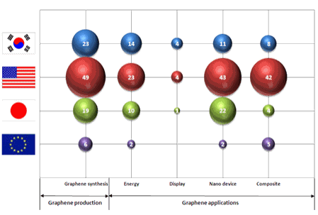
February 16, 2011 — Displaybank’s latest report covers graphene technology patents registered in Korea, U.S., Japan, and Europe by August 20, 2010. Valid patents corresponding to graphene manufacturing and applications are culled from 891 items of raw data.
 
Graphene manufacturing technology is divided into graphene synthesis, graphene film, and graphene complex. Graphene application device is divided into energy device, display device, electronic device, and BT-related device. 
 
R&D activities regarding graphene are on the rise. They exist in various fields: chemical, material, and mechanical. Graphene is expected to be widely applied since it has high carbon-chemical stability and electroconductivity. Physical properties lend graphene to use in basic science R&D — such as research on the Higgs boson particle — and potentially applied-R&D materials. To realize graphene’s potential, economical mass production techniques are needed.

Click to Enlarge

Figure. Patent application status by technology and country. Source: Displaybank February 2011.

The report covers patent application trends, major regions working on graphene, and major graphene patent applicant’s, namely Samsung, activities.

Learn more about the patent analysis here: http://www.displaybank.com/eng/report/report_show.php?id=729
 

Follow Small Times on Twitter.com by clicking www.twitter.com/smalltimes. Or join our Facebook group

February 16, 2011 – BUSINESS WIRE — CVD Equipment Corporation (Nasdaq: CVV) announced that new orders received during January 2011 totaled approximately $9.3 million dollars. These orders are for both production and research equipment in the fields of solar photovoltaics (PV), LEDs and nanotechnology.

Leonard Rosenbaum, president of CVD Equipment Corporation, states:
We are very pleased by the significant level of new orders received in January 2011 for both production and research equipment. We will continue to expand our research product offerings and develop optimized production equipment for our customers. As our research equipment customers transition from research to production, CVD will continue to be an integral part of their success. The CVD/FN division continues to benefit from increased interest and funding in energy generation, energy savings and nanotechnology for both research and production equipment. We anticipate that this interest will continue throughout 2011.

To support our continued and projected growth, our Board of Directors has taken the prudent step of filing a Form S-3 registration statement with the U.S. Securities and Exchange Commission, commonly known as a "shelf registration." When the shelf registration statement is declared effective by the SEC, the Company, at its option, will have the ability to conduct registered offerings of up to $20 million of common stock, preferred stock, debt securities, warrants to purchase these securities, unit offerings or any combination of such securities in multiple transactions over a period of up to three years.

To be clear, we currently have an ample amount of cash and positive operating cash-flow. However, we realize that to meet increasing order levels and minimize segment risk, we may need to raise capital to support the expansion of product offerings, personnel, equipment and facilities. If we choose to sell shares under this shelf registration, it will be at a price we deem favorable to the Company, shareholders and for the purpose of financing both short and long term growth opportunities. For the above reasons, we believe this shelf filing is beneficial to the Company and its shareholders as it allows the Company to raise the capital as needed to continue our current and anticipated growth.

Specific terms of any future offering under this registration statement will be established at the time of any such offering and will be described in a prospectus supplement that the Company would at such time file with the SEC.

CVD Equipment Corporation (NASDAQ: CVV) is a designer and manufacturer of standard and custom state-of-the-art equipment used in the development, design and manufacture of advanced electronic components, materials and coatings for research and industrial applications. CVD offers a broad range of chemical vapor deposition, gas control, and other equipment that is used by customers to research, design and manufacture semiconductors, solar cells, carbon nanotubes, nanowires, LEDs, MEMS, industrial coatings and equipment for surface mounting of components onto printed circuit boards. Learn more at www.cvdequipment.com

Follow Small Times on Twitter.com by clicking www.twitter.com/smalltimes. Or join our Facebook group

February 16, 2011 — The realization of self-powered microsystems for medical implants, drug delivery, remote monitoring, or safety-driven applications forms the basis behind a new project being run at the UK’s NPL by the Functional Materials Group. The goal is to replace batteries in these applications with an energy-scavenging power supply.

This energy harvesting power supply would eliminate the environmental hazards and costs associated with battery technologies. Energy harvesting covers the scavenging of many low-grade energy sources such as environmental vibrations, human power, thermal sources, wind energy and their conversion into useable electrical energy.

This project is concerned mainly with environmental vibrations and human power, where the transformation of mechanical to electrical energy is used to power small autonomous devices. The conversion can be achieved by various methods; however, the most promising options for MEMS devices include magnetic, piezoelectric and magnetostrictive transformation.

Example applications might include airborne particle detection in massively parallel autonomous sensing systems (motes), medical condition monitoring with embedded active drug delivery systems, and the development of structural health monitoring systems that scavenge innate vibrations for self power.

The global market for microsystems technology is estimated at $35 billion (2002 – Nexus: Market analysis for MST 2000-2005), with biomedical applications estimated at EU12B.There are a wide range of UK companies that would benefit from this understanding of this technology, from healthcare to transport, the energy sector, aerospace and defense sectors, where MST is given a high priority. The expected time frame during which this technology will be demonstrated extends from 2 to 5 years for defense applications associated with the Smart Soldier concept to 3-7 years for domestic appliances (MP3 players with built-in energy scavengers for example).

Knowledge will be shared with all partners onboard the project, whilst the wider community will enjoy open access to the generic metrology output in the form of web-based tools, new pre-normative standards documents, and the work will be further assessed for quality through the peer-reviewed publication process. Case studies will demonstrate the concepts so that organizations not in the materials supply market will gain a better understanding of the benefits associated with energy harvesting.

Read more in the recent edition of NPL’s Environmental Measures at http://www.npl.co.uk/publications/newsletters/

The National Physical Laboratory (NPL) is the UK’s National Measurement Institute and is a world-leading centre of excellence in developing and applying the most accurate measurement standards, science and technology. Read about NPL’s Functional Materials research at http://www.npl.co.uk/advanced-materials/materials-areas/functional/

Follow Small Times on Twitter.com by clicking www.twitter.com/smalltimes. Or join our Facebook group