Tag Archives: Small Times Magazine

February 15, 2011 — The University of South Florida received $5.45 million in grants from the Bill & Melinda Gates Foundation to create advanced devices that mimic the human liver to better study the life cycle of the malaria parasite, and to develop effective therapies for the disease.

Malaria may be most vulnerable to attack in the liver stage. Human models fabricated on micromechanical systems could help accelerate the discovery of new drugs or even vaccines for Plasmodium vivax and Plasmodium falciparum, the two most common forms of malaria.

Effective therapeutics funded in the second grant target malaria preventions and cure by a long-term continuous culture system for P. vivax.
Click to Enlarge
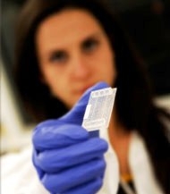
Photo 1. A microfluidic device used to create human mimetic tissue models for testing potential malaria drugs.

USF will collaborate with Draper Laboratory on the projects. The dynamic public-private partnership combines the USF Global Infectious Disease Research team’s expertise in malaria parasite biology and human model development with Draper’s extensive experience in tissue engineering and the development of human mimetic in vitro (laboratory) models. Draper Lab has been involved in MEMS research and development since 1984, including multiple biological applications.

To create new models to mimic human body conditions in which malaria parasites replicate, the researchers are using Draper’s prototype microfluidic device technology. The microfluidic device consists of microscope slide-sized unit containing chambers through which fluid flow is maintained by a micro-pump.  It is designed to support complex tissue growth, allowing liver or blood vessel cells to grow in three dimensions while experiencing physiologically relevant forces instead of on the static two-dimensional surface of a petri dish.  This technology, previously unavailable in a lab setting, may also prove useful for screening large volumes of potential anti-malarial agents and evaluating their effectiveness. Also read: MEMS may screen metastatic breast cancer cells by mimicking environment

"The Draper models offer unique microenvironments, so cells grow and function more normally," said Dennis Kyle, Ph.D., professor of global health at the USF College of Public Health. "That’s important because one major roadblock to learning about the liver stage of the malaria parasite has been that the liver cells lose some of their basic functions and no longer metabolize drugs after a few days."

"We cannot eliminate one of the most prevalent causes of malaria in the world — Plasmodium vivax — unless we come up with new drugs or vaccines that target the dormant liver forms of the parasite," Dr. Kyle said. "Current tools– in vitro and animal models are either largely ineffective or cost-prohibitive in predicting which drugs may work best in humans. New human models are the basic building blocks needed to establish strong, credible drug and vaccine discovery programs, not only at USF but at other universities and companies working on new ways to fight malaria."

Dr. Kyle is the principal investigator for a three-year Gates Foundation grant seeking to develop human liver models that could more quickly and accurately test potential drug candidates for vivax and falciparum malaria. Draper Laboratory’s efforts will be overseen by principal investigator Joseph Cuiffi, PhD, of the Draper Bioengineering Center at USF. They are working with John Adams, Ph.D., professor of global health at USF; Jeffrey Borenstein, Ph.D., a Draper physicist and biomedical engineer; and Joseph Charest, Ph.D., a Draper biomedical engineer. The original work on this technology at Draper was funded by the Center for the Integration of Medicine and Innovative Technology of which Draper is a founding member.
Click to Enlarge

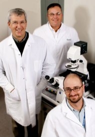
Photo 2. Clockwise from left: Principal investigators Dr. John Adams and Dr. Dennis Kyle of USF Health are collaborating on the Gates Foundation-funded projects with Dr. Joseph Cuiffi, principal investigator at Draper Lab.

Dr. Adams is the principal investigator for a three-year Gates Foundation grant that brings together a worldwide network of leading investigators with the skills and resources needed to create long-term blood stage cultures of vivax malaria. This form of malaria has proven particularly difficult to grow and sustain in the laboratory. Dr. Adams is working with Dr. Cuiffi and Dr. Kyle, as well Dr. Jetsumon (Sattabongkot) Prachumsri of the Vivax Research Center in the Faculty of Tropical Medicine, Mahidol University, and the Armed Forces Research Institute in Bangkok, Thailand; Dr. Peter Siba, director of the Papua New Guinea Institute for Medical Research; Dr. Louis Schofield, a Howard Hughes Medical Institute international research scholar at the Walter and Eliza Hall Institute of Medical Research in Australia; and Dr. Osamu Kaneko at Nagasaki University in Japan.

"To be able to replicate and study the entire malaria infection process outside the body will be critical in developing new drugs with the potential to eliminate malaria," said Draper’s Dr. Cuiffi.

Malaria and the liver
Malaria affects 10% of the world’s population, killing nearly one million people a year in developing countries and crippling their economies. In humans, the liver is the first target of the disease once a person is bit by an infected mosquito. The infecting parasites for most types of malaria multiply and rupture liver cells, escaping back into the bloodstream. In vivax malaria, some parasites can remain dormant in the liver for extended periods before infecting the blood.  The parasites, now modified to attack red blood cells, rapidly create more parasites, which spread throughout the bloodstream in waves.

At this initial stage of human infection there are fewer parasites — hundreds or a few thousand in the liver compared to millions once parasites start replicating in the bloodstream. Vivax has the potential to lay dormant in the liver and re-activate months or years after treatment, causing relapses of malaria. While parasites are in the liver, the person does not feel sick. Once parasites enter the bloodstream, disease symptoms emerge. "The drugs available to treat the bloodstream stages don’t work in the liver," Dr. Adams said. "So if you could get rid of parasites in the liver stage, you could essentially prevent vivax malaria and the transmission of infection."

Third, the only drug effective in attacking the liver’s reservoir of dormant malaria parasites to help prevent recurrences of vivax malaria, Primaquine, is risky for widespread use. Administering Primaquine to people with a red blood cell enzyme deficiency, known as glucose phosphate dehydrogenase (G6PD) deficiency, may trigger severe and potentially lethal blood loss, Dr. Adams said. "There’s no good bedside test to identify G6PD-deficient individuals, and, unfortunately, this condition most often occurs in those areas where vivax malaria is endemic."

More information on Draper Laboratory MEMS work is available at http://www.draper.com/mems_background/index.html. Learn more about the University of South Florida at www.usf.edu

Follow Small Times on Twitter.com by clicking www.twitter.com/smalltimes. Or join our Facebook group

NEi Software debuts FEA app


February 15, 2011

February 15, 2011 — NEi Software debuts its free finite element analysis (FEA) mobile application, NEi Stratus, experimenting with how and when finite element analysis solutions can be delivered to engineers. With this current application, finite element analysts can explore how mobile technology can be used to perform basic analysis, viewing results on their Apple iPhone and iPad anywhere and anytime.

The company sees the potential of combining cloud technology with the power of NEi Nastran solvers and believes this initial exploration into the combination will allow for more complex analysis as the technology matures.
 
NEi Stratus will be available by the beginning of the second fiscal quarter and will be initially offered at no charge. Those interested in viewing demos of this free mobile FEA application can visit http://www.nenastran.com/mobile.

NEi Software recognized two rapidly advancing technologies that have great potential within the computer-aided engineering (CAE) industry: mobile applications and cloud computing. "NEi Stratus leverages these technologies to give engineers on-demand Nastran-based analysis," said Mitch Muncy, manager of presales and technical support for NEi Software.

NEi Software is a CAE supplier offering Nastran FEA, engineering simulation, and virtual testing software. Learn more at http://www.nenastran.com

Follow Small Times on Twitter.com by clicking www.twitter.com/smalltimes. Or join our Facebook group
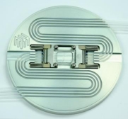
February 14, 2011 — Dolomite, microfluidic designer and manufacturer, expanded its range of temperature control systems with the Hotplate Adaptor – Chip Holder H, which allows control over internal temperatures of microfluidic chips without any disruptions to the fluid flow.

Click to Enlarge Click to Enlarge Click to Enlarge

The use of temperature control systems is vital for many applications including nanostructure generation, controlled microreactions, and droplet microfluidics where droplets can be kept at certain temperature to prevent a solidification reaction until the droplets have left the chip.

Holding a microfluidic chip securely in position, the Hotplate Adaptor enables users to pre-heat or post-heat fluids by using the integrated tube heater. Operating over a temperature range up to 100°C, the adaptor is supplied with a removable lid that can be closed to maintain the chip at constant temperatures, which is important for cell-based analytical studies to maintain cell viability. A glass viewing window (22mm in diameter) facilitates microscopic observations.

Quick and easy to use, the Hotplate Adaptor has been specifically developed for the Chip Interface H, and is compatible with Dolomite’s Linear Connector 4-way, 1.6mm tubing and microfluidic chips that have a footprint of 22.5 x 15mm.

Dolomite is pioneering the use of microfluidic devices for small-scale fluid control and analysis, enabling manufacturers to develop more compact, cost-effective and powerful instruments. By combining specialist glass, quartz and ceramic technologies with knowledge of high performance microfluidics, Dolomite is able to provide solutions for a broad range of application areas including environmental monitoring, clinical diagnostics, food and beverage, nuclear, agriculture, petrochemical, cosmetics, pharmaceuticals and chemicals. Dolomite’s in-house micro-fabrication facilities include clean rooms and precision glass processing facilities. For more information please visit www.dolomite-microfluidics.com

Follow Small Times on Twitter.com by clicking www.twitter.com/smalltimes. Or join our Facebook group

February 14, 2011 — In a study published in Nature Nanotechnology, researchers from The University of California Los Angeles (UCLA) Henry Samueli School of Engineering and Applied Science and from the materials division of Australia’s University of Queensland show the promise of surface-conduction channels in topological insulator nanoribbons made of bismuth telluride and demonstrate that surface states in these nanoribbons are "tunable" able to be turned on and off depending on the position of the Fermi level.

"Our finding enables a variety of opportunities in building potential new-generation, low-dissipation nanoelectronic and spintronic devices, from magnetic sensing to storage," said Kang L. Wang, the Raytheon Professor of Electrical Engineering at UCLA Engineering, whose team carried out the research.

Topological insulators act as both insulators and conductors, with their interior preventing the flow of electrical currents while their edges or surfaces allow the movement of a charge. The surfaces of topological insulators enable the transport of spin-polarized electrons while preventing the "scattering" typically associated with power consumption, in which electrons deviate from their trajectory, resulting in dissipation.

Because of such characteristics, these materials hold great potential for use in future transistors, memory devices and magnetic sensors that are highly energy efficient and require less power.

Bismuth telluride (BiTe) is well known as a thermoelectric material and has also been predicted to be a three-dimensional topological insulator with robust and unique surface states. Recent experiments with bismuth telluride bulk materials have also suggested two-dimensional conduction channels originating from the surface states. But it has been a great challenge to modify surface conduction, because of dominant bulk contribution due to impurities and thermal excitations in such small band-gap semiconductors.

The development of topological insulator nanoribbons has helped. With their large surface-to-volume ratios, these nanoribbons significantly enhance surface conditions and enable surface manipulation by external means.

Wang and his team used thin bismuth telluride nanoribbons as conducting channels in field-effect transistor (FET) structures. These rely on an electric field to control the Fermi level and hence the conductivity of a channel. The researchers were able to demonstrate for the first time the possibility of controlling surface states in topological insulator nanostructures.

"We have demonstrated a clear surface conduction by partially removing the bulk conduction using an external electric field," said Faxian Xiu, a UCLA staff research associate and lead author of the study. "By properly tuning the gate voltage, very high surface conduction was achieved, up to 51%, which represents the highest values in topological insulators."

"This research is very exciting because of the possibility to build nano devices with a novel operating principle," said Wang, who is also associate director of the California NanoSystems Institute (CNSI) at UCLA. "Very similar to the development of graphene, the topological insulators could be made into high-speed transistors and ultra-high-sensitivity sensors."

The new findings shed light on the controllability of the surface spin states in topological insulator nanoribbons and demonstrate significant progress toward high surface electric conditions for practical device applications. The next step for Wang’s team is to produce high-speed devices based on their discovery.

"The ideal scenario is to achieve 100% surface conduction with a complete insulating state in the bulk," Xiu said. "Based on the current work, we are targeting high-performance transistors with power consumption that is much less than the conventional complementary metal-oxide semiconductors (CMOS) technology used typically in today’s electronics."

Study collaborators Jin Zou, a professor of materials engineering at the University of Queensland; Yong Wang, a Queensland International Fellow; and Zou’s team at the division of materials at the University of Queensland contributed significantly to this work. A portion of the research was also done in Alexandros Shailos’ lab at UCLA.

The study was funded by the Focus Center Research Program Center on Functional Engineered Nano Architectonics (FENA) at UCLA Engineering; the U.S. Defense Advanced Research Projects Agency (DARPA); and the Australian Research Council. The research on topological insulators was pioneered by FENA’s Shoucheng Zhang, a professor of physics at Stanford University.

The UCLA Henry Samueli School of Engineering and Applied Science offers 28 academic and professional degree programs and has an enrollment of almost 5,000 students. The school’s distinguished faculty are leading research to address many of the critical challenges of the 21st century, including renewable energy, clean water, health care, wireless sensing and networking, and cyber-security. UCLA Engineering is home to seven multi-million-dollar interdisciplinary research centers in wireless sensor systems, nanoelectronics, nanomedicine, renewable energy, customized computing, and the smart grid, all funded by federal and private agencies. Learn more at http://www.ucla.edu/

Courtesy of Wileen Wong Kromhout, UCLA

Fluidigm prices FLDM IPO


February 14, 2011

February 14, 2011 – BUSINESS WIRE — Fluidigm Corporation priced its initial public offering (IPO) of 5,558,333 shares of its common stock at a price to the public of $13.50 per share. The shares of common stock have been approved to trade on The NASDAQ Global Market under the symbol FLDM.

Deutsche Bank Securities Inc. and Piper Jaffray & Co. are acting as joint book-running managers for the offering. Cowen and Company LLC and Leerink Swann acted as co-managers. Fluidigm has granted the underwriters an option to purchase up to an additional 833,750 shares of common stock to cover over-allotments, if any.

A registration statement relating to these securities was declared effective by the Securities and Exchange Commission (SEC) on February 9, 2011.

This offering is being made solely by means of a prospectus, copies of which may be obtained from: Deutsche Bank Securities Inc., Attn: Prospectus Department, 100 Plaza One, Floor 2, Jersey City, NJ 07311, or by calling (800) 503-4611 or emailing a request to [email protected] or by contacting Piper Jaffray & Co. at 800 Nicollet Mall, Suite 800, Minneapolis, MN 55402, by calling 1-800-747-3924.

Fluidigm develops, manufactures, and markets microfluidic systems for growth markets in the life science and agricultural biotechnology (Ag-Bio) industries. Fluidigm’s proprietary microfluidic systems consist of instruments and consumables, including chips and reagents. Fluidigm actively markets three microfluidic systems including eight different commercial chips to leading pharmaceutical and biotechnology companies, academic institutions, diagnostic laboratories and Ag-Bio companies. For more information, please visit www.fluidigm.com

Company Disclaimer: This press release shall not constitute an offer to sell or a solicitation of an offer to buy, nor will there be any sale of these securities in any state or jurisdiction in which such an offer, solicitation, or sale would be unlawful prior to registration or qualification under the securities laws of any such state or jurisdiction.

Follow Small Times on Twitter.com by clicking www.twitter.com/smalltimes. Or join our Facebook group

February 11, 2011 — Vistec Lithography Inc., advanced electron-beam lithography equipment provider, received an order from the ETH Zurich (Swiss Federal Institute of Technology), a world-renowned research university, for one of its Vistec EBPG5200 systems. The Vistec EBPG5200 will be installed in the new Nanotechnology Center, which is a public/private partnership between IBM Research – Zurich and ETH Zurich.

ETH Zurich will focus on exploratory research aiming at nanotechnology applications as MEMS/NEMS, nanowires, carbon-based devices, functional materials, optical interconnects, photonics and directed self-assembly, among other areas.

According to the evaluation team, the primary reason the Nanotechnology Center selected the Vistec system is the advanced technology capabilities it offers. "Our multiple research applications require a high performance nano-patterning tool of superior flexibility, which is essential for extending our advanced R&D efforts," said the evaluation team representative.

The Vistec EBPG5200 is the latest version of the EBPG electron-beam lithography tool series. The EBPG5200 system can be operated with 20, 50 and 100kV accelerating voltage and is equipped with a 50MHz pattern generator and full 20bit address technology. Thanks to further enhancements in resolution, noise reduction and beam stability, the Vistec EBPG5200 is set to routinely generate structures less than 8nm on varying substrates sizes from piece parts of a few millimetres to full patterning across a 200mm diameter. The system incorporates an interactive graphical user interface (GUI) that provides ease of use for diverse multi user environments.

Vistec Lithography develops, manufactures, and sells electron-beam lithography equipment based on Gaussian Beam technology. Learn more at www.vistec-semi.com

Follow Small Times on Twitter.com by clicking www.twitter.com/smalltimes. Or join our Facebook group
February 11, 2011 – PRNewswire — STMicroelectronics (NYSE: STM), semiconductor and MEMS sensor manufacturer, and bTendo Ltd. signed a development and license agreement to jointly develop the world’s smallest pico projector for smart phones and other portable consumer-electronics devices. It will be based on bTendo’s innovative Scanning Laser Projection engine technology and ST’s micro electro mechanical systems (MEMS) expertise, video processing know-how and semiconductor process technology.

Less than 2.5cm3 in volume and below 6mm high, the jointly developed embedded projector solution will offer a focus-free, vivid color, sharp and crisp image, superior to current pico projection solutions. Implementing two MEMS-based micro-mirror-actuation devices within the system’s optical engine, and an advanced video-processing chip, the miniature projection engine is optimized for smart phones, offering low power consumption and built-in support for mobile industry processor interface (MIPI) to ensure swift and easy integration.

With today’s advanced smart phones, people carry huge amounts of movie clips and photos in their pockets, yet find it difficult sharing it with others due to the tiny display. Adding projection capabilities into the mobile devices will enable users to easily share their media with others in any place, on any surface, at any time, the companies say.

"People want to share their media with others and enjoy the option of expanding their display even for their own personal viewing," said Benedetto Vigna, Group VP and GM, MEMS, Sensor and High-Performance Analog Division, STMicroelectronics. "ST selected bTendo’s technology due to its small size, low power and focus-free features, which are all critical for embedded projection modules. ST has a long history in the development of innovative technologies and this joint cooperation will further extend our MEMS sensor expertise, while also complementing and reinforcing our leadership in MEMS gyroscopes and accelerometers for advanced user interfaces."

"We are very excited to collaborate with STMicroelectronics, the world leader in MEMS technologies for mobile handsets, to bring to market our cutting-edge technology for embedded Pico Projectors," said Dana Gross, CEO of bTendo Ltd. "ST’s best-in-class semiconductor process technology and design capabilities will enable a cost-effective, low-power solution perfect for personal consumer devices."

A demo of the technology will be shown at Mobile World Congress in Barcelona, Feb 14-17, 2011 on the STMicroelectronics stand (7A106).

STMicroelectronics serves customers across the spectrum of electronics applications with innovative semiconductor solutions. Further information on ST can be found at www.st.com.

bTendo is a developer of personal projection technologies and solutions. For more information www.btendo.com

Also read: Introduction to MEMS gyroscopes by Jay Esfandyari, Roberto De Nuccio, Gang Xu, STMicroelectronics

Follow Small Times on Twitter.com by clicking www.twitter.com/smalltimes. Or join our Facebook group
February 10, 2011 — Capitalizing on their design wins in Apple Inc.’s iPhone 4 and iPad, semiconductor suppliers STMicroelectronics and TriQuint in 2010 achieved industry-leading growth in the global market for microelectromechanical systems (MEMS) in consumer electronics and mobile devices, new IHS iSuppli research indicates.

TriQuint’s revenue in this area expanded by 778.6% in 2010, with its consumer and mobile MEMS revenue amounting to $74.7 million in 2010, up from a negligible $8.5 million in 2009. This propelled TriQuint to the No. 8 ranking in the market, up from 16th place in 2009. STMicroelectronics posted the second-highest growth rate among the Top 10, with its revenue rising by 63.5%. The company’s revenue amounted to $353.6 million, up from $216.3 million in 2009, allowing it to expand its leadership in global consumer and mobile MEMS sales.

Read iSuppli’s report about MEMS in the iPhone

The iPhone 4 includes five separate MEMS devices, plus a third MEMS microphone in the headset, up from two in the iPhone 3GS.

The iPad 3G contains three MEMS devices.

The iPhone 4 and iPad 3G integrated TriQuint’s TQM666092 transmit module for the WCDMA band 2, which consist of a single-band power amplifier, a bulk acoustic wave (BAW) duplexer and a surface acoustic wave (SAW) interstage filter. The company launched its MEMS BAW filter technology early in 2009 and by 2010 managed to grab 26% of the global BAW market from Avago.

The iPhone 4 also includes STMicroelectronics’ LIS331DLH MEMS accelerometer, and its L3G4200D MEMS digital three-axis gyroscope.

The gyroscope design win in the iPhone 4 played an important role in STMicroelectronics’ massive revenue increase in 2010, serving as a new growth market for the company’s MEMS line.

STMicroelectronics accounted for 50% of global accelerometer revenue during the past two years, and its share is not likely to rise significantly in the future. Meanwhile, growth is slowing in the accelerometer market.

Because of this, STMicroelectronics has sought new growth drivers, investing heavily in gyroscope development in 2008 and 2009. This paid off in 2010 as gyroscopes brought in $117 million of revenue for the company and contributed to 85% of STM’s consumer MEMS revenue growth. The IHS iSuppli Teardown Analysis Service also identified STMicroelectronics’ 3-axis gyroscope in the iPad, the fourth-generation iPod Touch, the Samsung Galaxy Tab and the Sony Move controller.

The company is paving the way for its next growth engines by offering MEMS microphones and MEMS pressure sensors for handsets and tablets, which should contribute to revenue starting this year.

Read more…

Follow Small Times on Twitter.com by clicking www.twitter.com/smalltimes. Or join our Facebook group

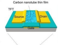
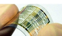
February 10, 2011 — Research teams for Professor Yutaka Ohno Nagoya University (Japan) and Prof. Esko I. Kauppinen, Aalto University (Finland), have developed a simple and rapid technique to fab carbon nanotube (CNT) thin film transistors on plastic film.

Click to Enlarge

The researchers believe they have produced the world’s first carbon nanotubes based on sequential logic integrated circuits (ICs). In the recently developed method, nanotubes are grown using gas phase filtration and thin film transfer to the crucible of plastic on top. This creates a clean and uniform film in a few seconds, researchers report. This method could further be developed into a high-speed roll-to-roll (R2R) manufacturing process.

The inventors believe that the developed carbon nanotube manufacturing process will allow for flexible electronics, such as electronic paper, made at competitive production rates. 

Click to Enlarge

Interest in lightweight and flexible devices, such as a flexible mobile phone and electronic paper, has increased recently. These devices require flexible electronics components, produced cheaply and quickly directly onto plastic substrates.

Carbon nanotubes offer good conductivity and chemical stability, but current CNT manufacturing does not result in CNT transistors with the properties expected. Nanotubes manufactured in the current synthesis process are partially destroyed, whereas the gas phase filtration process leaves them whole, say researchers.

Research results were published in the February 6, 2011 issue of Nature Nanotechnology: http://www.nature.com/nnano/index.html

The study was funded by the New Energy and Industrial Technology Development Organization (Nedo), Japan and the Aalto University Multidisciplinary Institute of Digitalization and Energy Research (MIDE).

For more information, visit http://electronics.tkk.fi/fi/ajankohtaista/uutiset/view/hiilen_nanoputket_valmistettu_muovikalvolle/

Follow Small Times on Twitter.com by clicking www.twitter.com/smalltimes. Or join our Facebook group

February 10, 2011 – Marketwire — The Optoelectronics Research Centre (ORC) at the University of Southampton, U.K., purchased a DPN 5000 System from NanoInk’s NanoFabrication Systems Division to be used for the fabrication of nanostructured photonic metamaterials, nanophotonics and sensors.

NanoInk’s DPN 5000 System is a full-featured, dedicated instrument for versatile nanopatterning of a variety of materials with nanoscale accuracy and precision. With its user-friendly interface, it is possible to easily design complex patterns while also precisely controlling the tip movements during the writing process. Dip Pen Nanolithography (DPN) is a patented and proprietary nanofabrication technology.

"NanoInk’s DPN 5000 system provides unique advantages in terms of materials deposition capability and scalability and we believe that many exciting research and commercial opportunities will develop from this technology," said Dr. Kevin MacDonald, senior research fellow at the ORC. "It will be particularly important in the development of our research on nanophotonics, metamaterials and optical sensors."

"The DPN 5000 enhances the Optoelectronics Research Centre’s world class nanoscale research in the areas of applied photonics and nanotechnology. It has the ability to deliver unique capabilities in new areas of research, including nanobiology applications," said Robert Marchmont, GM of Europe, the Middle East and Africa for NanoInk.

NanoInk’s NanoFabrication Systems Division brings sophisticated nanofabrication to the laboratory desktop in an easy to use and affordable setting. It provides the ability to design and create custom engineered and functionalized surfaces with nanometer-scale precision and sub-cellular resolution. NanoInk, Inc. is an emerging growth technology company specializing in nanometer-scale manufacturing and applications development for the life sciences, engineering, pharmaceutical, and education industries. More information is available on its new Web site at: www.nanoink.net/divisions.html#NanoFabrication

The Optoelectronics Research Centre is a leading institute for photonics research based at the University of Southampton. It comprises more than 30 groups working in areas from optical materials discovery and fundamental photonics to light generation and advanced optical fiber technologies. More information is available at: www.orc.soton.ac.uk.

Follow Small Times on Twitter.com by clicking www.twitter.com/smalltimes. Or join our Facebook group