Tag Archives: Small Times Magazine

February 10, 2011 – Marketwire — SPP Process Technology Systems (SPTS), plasma etch, deposition, and thermal processing equipment manufacturer for the micro-device industry, completed the acquisition of deep reactive ion etch (DRIE) technology and certain related assets from Tegal Corporation. In addition, the deal includes the transfer to SPTS of the capital stock and operations of Tegal France SAS, a wholly-owned Tegal subsidiary formed by Tegal’s acquisition of Alcatel Micro Machining Systems’ DRIE assets in September 2008.

SPTS’ acquisition will include the Tegal DRIE product line (including 200, 110, 3200, and 4200 series), along with the Compact and Pluto development assets, intellectual property (IP) and process know-how. SPTS will provide continued global support to existing Tegal DRIE customers, and will integrate these technologies into its SPTS’ broad range of product offerings in etch, deposition and thermal technologies. SPTS just days ago acquired the etch portfolio of Primaxx from its parent company.

"The sale of the Tegal DRIE assets to SPTS secures our technology, team members, active joint development projects in France, and ensures continuation of our commitments to customers globally," said Thomas Mika, president and CEO, Tegal Corporation. "This event represents another major step in Tegal’s transformation from semiconductor capital equipment supplier to its new role in providing green energy." Tegal recently announced participation in the formation of sequel Power, a company engaged in large scale photovoltaic (PV)-based solar utilities.

SPP Process Technology Systems was established in October 2009 as the vehicle for the merger of Surface Technology Systems and acquired assets of Aviza Technology. The company is a wholly-owned subsidiary of Sumitomo Precision Products Co., Ltd., and designs, manufactures, sells, and supports advanced semiconductor capital equipment and process technologies for the global semiconductor industry and related markets. These products are used in a variety of market segments, including R&D, data storage, MEMS and nanotechnology, advanced 3-D packaging, LEDs, and power integrated circuits for communications. For more information about SPTS, please visit www.spp-pts.com.

Tegal is dedicated to the development and application of both proven and emerging technologies in the field of green energy. Tegal is engaged in the promotion of solar power plant development projects worldwide, the development of self-sustaining businesses from such projects, including supporting, developing, building and operating solar photovoltaic fabrication facilities and solar farms and other non-PV based renewable energy projects. Learn more at www.Tegal.com.

Subscribe to Solid State Technology/Advanced Packaging.

Follow Solid State Technology on Twitter.com via editors Pete Singer, twitter.com/PetesTweetsPW and Debra Vogler, twitter.com/dvogler_PV_semi.

Or join our Facebook group

February 9, 2011 — GIA released a comprehensive global report on microscopes markets. The global market for microscopes is forecast to exceed US$2.4 billion. Key factors driving market growth include technological advancements, increasing end-user demand for premium quality imaging, and surging demand from industrial and biological sectors. Further, advancements in material sciences have also helped propel the use of microscopes.

Over the years, the global market for microscopes has largely been driven by the increased demand from the industrial and biological sectors. Developments in areas involving semiconductors, micro electrical mechanical systems (MEMS), nanotechnology and other material sciences have also helped propel the use of microscopes. Increased demand for high-quality, precision imaging from various end-user sectors further boosted the demand for advanced microscopes such as electron microscopes, and SPMs.

However, during 2008-2009 the global market for microscope reeled under the impact of recession that hampered the growth of the market to a significant extent. Among the various types of microscopes, scanning-probe and charged particle microscopes were severely hit by the recession, as the microscopes are largely used in semiconductor industry. Nevertheless, the rapidly evolving imaging technologies and growing requirements of the researchers, advancements in confocal and electron microscopy, cytometry, laser scanning, and the developments in the quantum dots area are expected to play a major role in boosting the demand for microscopes in the near future.

Geographical consumption

The US constitutes the largest regional market for microscopes worldwide, as stated by the new market research report on microscopes. Japan represents the other major market for microscopes, and the two countries collectively account for a major share of the total world microscopes market. However, Asia-Pacific is projected to be the fastest growing regional market for microscopes, with a CAGR of more than 3.0% over the analysis period. Rapid expansion of biomedical research and growth in the electronics and semiconductor production sectors are driving microscopes’ growth in the region.

Microscopes by type

Charged particle microscopes constitute the largest microscopes segment. Going forwards, demand for charged particle microscopes is likely to be driven by the advancements in material sciences and research and development fields, and increased substitution of optical microscopes by electron and other sophisticated microscopes in various applications. On the other hand, registering a CAGR of 2.6% over the analysis period, scanning probe microscopes represents the fastest growing product segment in the global microscopes market. Revival in demand of scanning probe microbes is heavily depended on the resurgence of semiconductor industry and growth in nanotechnology sector including various nanaoscale applications. Other major factors that are likely to bolster the demand for scanning probe and electron probe microscopes include increased complexities as well as performance levels of the devices that find use in electronic products, decreasing geometries, growing yields, and growing demand for enhanced failure analysis processes and techniques. Demand for optical microscopes, the other principal product segment, is likely to depend on the trends in the infrared spectroscopy sector, research and development in the life sciences sector, and spending on the material-science and educational equipment.

Digital imaging

A key trend in the microscopy industry in recent years has been the integration of digital imaging in microscopes. Image analysis has become the criterion for shaping the design of microscopes. Standard laboratory microscopes are constantly being replaced by integrated digital image-analysis microscope systems in academic research. Responding to the growing market demand, the market is bundled with microscopes, equipped with advanced image analysis features. The market offers sophisticated microscopes, integrated with digital cameras and software.

More information

Major players profiled in the report include Bruker Corporation, Carl Zeiss AG, FEI Company, Hitachi High Technologies America Inc, Jeol USA Inc, Leica Microsystems GmbH, Nikon Corporation, Olympus Corporation, Thermo Fisher Scientific Inc, among others.

The research report, "Microscopes: A Global Strategic Business Report" announced by Global Industry Analysts Inc., provides a comprehensive review of the microscopes markets, impact of recession on the markets, current market trends, key growth drivers, recent product introductions, recent industry activity, and profiles of major/niche global as well as regional market participants. The report provides annual sales estimates and projections for Microscopes market for the years 2007 through 2015 for the following geographic markets – US, Canada, Japan, Europe, Asia-Pacific, Middle East, and Latin America. Key segments analyzed include Optical Microscopes, Charged Particle Microscopes and Scanning Probe Microscopes. The global market is also analyzed by the following end-use applications – Semiconductor Manufacturing, Life Sciences, Materials, Nanotechnology, and Others. Also, a seven-year (2000-2006) historic analysis is provided for additional perspective. For more details about this comprehensive market research report, visit http://www.strategyr.com/Microscopes_Market_Report.asp

Follow Small Times on Twitter.com by clicking www.twitter.com/smalltimes. Or join our Facebook group

February 9, 2011 — Nanocarbon products include single-walled carbon nanotubes (SWCNT or MWNT) and multi-walled carbon nanotubes (MWCNT or MWNT), fullerenes, graphene, carbon nanofiber and nanodiamonds. Carbon nanotubes are microscopic, tube-shaped structures, which essentially have a composition of a graphite sheet rolled into a tube.

Carbon nanotubes have unique, interesting and potentially useful electrical and mechanical properties, and offer potential for various uses in electronic devices. Carbon nanotubes also feature extremely high electrical conductivity, very small diameters (much less than 100nm), large aspect ratios (i.e. length/diameter ratios greater than 1000), and a tip-surface area near the theoretical limit (the smaller the tip-surface area, the more concentrated the electric field, and the greater the field enhancement factor). These features make carbon nanotubes ideal for electron field emitters, white light sources, lithium secondary batteries, hydrogen storage cells, transistors, and cathode ray tubes (CRTs).

According to a recently published report from iRAP, Inc., ET-113: Production and Application of Carbon Nanotubes, Carbon Nanofibers, Fullerenes, Graphene and Nanodiamonds: A Global Technology Survey and Market Analysis, the production capacity for all products was 4,065 tons in 2010, and is expected to exceed 12,300 tons in 2015. The actual production was less than 25% of the capacity in 2010 and about 50% of the capacity in 2015. Total production value is estimated at about $435 million in 2010 and is expected reach a value of $1.3 billion in 2015.

Click to Enlarge
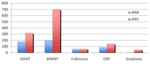
Share of nanocarbon production value according to types, 2010 and 2015 ($ Millions) Source: iRAP, Inc.

Production capacity far exceeds actual production. Only about 340 tons of carbon nano products were produced in 2008, about 500 tons in 2009 and about 710 tons are expected to have been produced in 2010, which represents about 17% of capacity. However, actual production is expected to reach more than 9300 tons in 2015, representing a growth rate of 67.3% annually and about 80% of production capacity.

Prices for all products are expected to fall by an average of about 12% a year for the next five years. Growth is chiefly driven by multi-walled carbon nanotubes. World production capacity for multi-wall carbon nanotubes exceeded 390 tons in 2008, reached 1,500 tons in 2009, and is estimated to exceed 3,400 tons per year (tpy) by the end of 2010. Production capacity for MWNT is projected to reach 9,400 tons by 2015. 

SWCNTs are the most expensive nano carbon product. They are much more difficult to produce than MWCNTs and are best suited for electronic applications. In 10 to 15 years, SWCNT are expected to replace silicon as the key material in computer chips. 

Despite the quickly growing capacity for CNTs, demand has not yet caught up with capacity.  However, manufacturers have been increasing capacity to be ready to capitalize on that future demand, which is expected to grow rapidly over the next five to ten years. 

For both SWCNTs and MWCNTs, Asia’s production capacity is two to three times higher than that estimated for North America and Europe combined; Japan is the prominent leader in the production of MWCNTs, but China and Korea are rapidly catching up.  Use of CNTs in lithium-ion battery electrodes is the current driving force of ton-scale MWCNT production in Japan.

Nanocarbon production value according to types, through 2015 ($ Millions) Source: iRAP Inc.
  2010 2015 AAGR % 
(2010-2015)
SWNT 180 320 12.2
MWNT  105 700 46.7
Fullerenes 61 60 -0.33
CNF  88 144 10
Graphene  0.75 48 130
Total  435 1,272 24

More details of the report are available from Innovative Research and Products (iRAP), Inc., P.O. Box 16760, Stamford, CT 06905, USA, (203) 569-7909, [email protected] or at http://www.innoresearch.net/reportlist.aspx?cid=7

Follow Small Times on Twitter.com by clicking www.twitter.com/smalltimes. Or join our Facebook group

February 9, 2011 – BUSINESS WIRE — Sand 9, Inc., is planning volume launch of its MEMS oscillator technology for wireless applications. The company appointed Skyworks EVP Greg Waters to their Board of Directors, using his experience in wireless communications to help Sand 9 manage the transition from development to volume production.

Sand 9 is introducing a temperature compensated MEMS oscillator (TCMO), a MEMS timing device that achieves the performance required for wireless applications such as 3G/4G cellular and GPS. "Sand 9’s breakthrough technology has the potential to be truly disruptive in the wireless communications market," said Waters.

Waters is executive vice president and general manager, front-end solutions, for Skyworks Solutions, Inc. He joined the company in April 2003. Prior to joining Skyworks, Waters served as senior vice president of strategy and business development at Agere Systems, and previously held positions there as vice president of the Wireless Communications business, and vice president of the Broadband Communications business.

Sand 9 is a venture funded company dedicated to the design of precision timing technology that will dramatically improve the capabilities of electronic devices. The company’s investors include Commonwealth Capital, Flybridge Capital Partners, General Catalyst and Khosla Ventures. For more information, visit www.sand9.com.

Follow Small Times on Twitter.com by clicking www.twitter.com/smalltimes. Or join our Facebook group

February 8, 2011 – BUSINESS WIRE — ADA Technologies Inc. received an $70,000 contract from the U.S. Army for Phase I research into the development of advanced electrochemical ultracapacitor systems for use in hybrid electronic vehicles (HEVs) for high-power military applications.

ADA’s research will leverage its recent work funded by the National Science Foundation (NSF) in which new low-cost carbon nanotube (CNT) nanocomposite electrode materials were developed and proven in pouch-cell testing.

"ADA has considerable expertise in CNT nanotechnology. We expect the successful completion of this Phase I research to lead to development of ultracapacitors with the energy and power densities needed for military applications. In addition, these ultracapacitors will have safe operation over a wide temperature range and excellent cycle life," said Douglas Campbell, ADA R&D program manager.

ADA’s work will be performed in partnership with Maxwell Technologies, Inc., a commercial provider of ultracapacitors for HEV applications.

This material is based upon work supported by the US Army Tank-Automotive Research Development and Engineering Center (TARDEC) under Contract No. W56HZV-11-C-0058.

ADA Technologies Inc. is a research, development, and commercialization company that specializes in creating and converting innovative technologies to commercial successes. For more information, visit www.adatech.com

Also read: Destination Nano: Saluting nanotech’s defense apps  by news editor James Montgomery

Follow Small Times on Twitter.com by clicking www.twitter.com/smalltimes. Or join our Facebook group

February 8, 2011 – BUSINESS WIRE — Bruker announced the North American launch of its compact, fully automated and fast toxin identification system, pTD, or portable Toxin Detector. The benchtop, push-button pTD system is intended for smaller, field, and mobile laboratories for use by non-expert operators in homeland security applications.

The Bruker pTD system simplifies and accelerates detection of potential biological terror attack using toxins. The pTD system uses a lab-chip-based, fully automated enzyme-linked immunosorbent assay (ELISA) process that allows the simultaneous identification of five toxins with an order of magnitude better sensitivity than traditional techniques. The fully automated pTD includes controls to minimize false positive or negative alarms. Toxin identification and quality control take place in less than 30 minutes. Traditional PCR-based or proteomic fingerprinting identification technologies for the detection and identification of toxins in the field are insensitive and slow, or involve complicated sample preparation in specialized laboratories, according to Bruker.

The pTD system accepts liquid and solid samples and does not require any external sample preparation steps. Every sample is automatically checked for five toxins simultaneously using multiplexed, proprietary lab chips. Toxin identification is based on ELISA using highly specific antibodies, combined with an electrochemical readout. All sample preparation steps are performed automatically inside the lab chip, and the results are displayed on the control computer. Before shutdown, the system automatically decontaminates itself internally.

The pTD system, which has been co-developed with Analytik Jena AG, identifies the five toxins Botulinum Toxin A, B and E, as well as Ricin and Staphylococcus enterotoxin B on one chip. Additional toxin ID chips are under development.

Bruker Detection provides ruggedized, field analytical systems for chemical, biological, radiological, nuclear and explosives (CBRNE) detection. For more information on Bruker Detection Corporation and Bruker Corporation (NASDAQ: BRKR), please visit www.bruker.com

Other lab-on-chip news:
Personalized medicine: Imec proposes lab-on-chip for SNP detection in DNA 
Lab-on-chip project aims to diagnose cancer faster 
Lab-on-chip system could provide fast detection of single nucleotide variations in DNA

Follow Small Times on Twitter.com by clicking www.twitter.com/smalltimes. Or join our Facebook group

February 8, 2011 Carbon nanotubes (CNTs) have many attractive properties, and their structure and areas of application can be compared with those of graphene. To exploit these properties, however, it is necessary to have full control of the manufacturing process. Scientists at the University of Gothenburg successfully defended a thesis on this subject, "In Silco Studies of Carbon Nanotubes and Metal Clusters."

"Our results show that the metal particles that form the basis of the manufacture of carbon nanotubes must have a certain minimum size, in order for growth to start and to continue. It is also probable that the particles are in liquid form at a manufacturing temperature of around 800°C, even though the metals used may have much higher melting points," says Anders Börjesson from the Department of Physics at the University of Gothenburg.

The scientists used various computer models to study in detail properties that are difficult or impossible to examine in experimental conditions. While the diameter of the nanotubes is of the order of one billionth of a metre, and they can be as thin as a single carbon layer, the length of the tubes can extend from the nanometer scale up to several decimeters. Carbon nanotubes can be regarded as thin threads of pure carbon, whose length can be a billion times greater than their thickness.

Click to EnlargeThe thesis In Silco Studies of Carbon Nanotubes and Metal Clusters has been successfully defended. Supervisor: Professor Kim Bolton. The research has been a collaboration between the University of Gothenburg and the University of Borås. Link to the thesis: http://bada.hb.se/handle/2320/6908

For more information on this research, contact Anders Börjesson, Department of Physics, University of Gothenburg, at +46(0)31 786 9143, +46(0)70 240 1145, [email protected]

Courtesy of Anita Fors

Follow Small Times on Twitter.com by clicking www.twitter.com/smalltimes. Or join our Facebook group

February 8, 2011 — The Global School for Advanced Studies (GSAS) invites post-doctorate fellows and other senior student researchers from around the world to apply for the June 20-26 session on "Graphene Fundamentals and Applications" in Grenoble, France.

Selected students, who will receive full travel and lodging support, will compete for fellowships to implement graphene-related research at CEA in Grenoble beginning in January 2012.

Hosted by the GIANT Innovation Campus in Grenoble, this program will create several research teams and challenge them to design a project based on graphene that will leverage their complementary strengths. Each team will have members from around the world and a balance of capabilities, including materials synthesis, characterization, device design and fabrication, theory and measurement.

Teams participating in the Graphene Fundamentals and Applications Session will receive project mentoring from leading global experts. These include Harry Kroto, a Nobel Prize winning professor in the Department of Chemistry and Biochemistry at Florida State University; Sumio Iijima, research fellow at NEC and a professor of materials science at Meijo University in Nagoya who is credited with discovering carbon nanotubes; and Daniel Neumaier, of AMO Research Foundry, and coordinator of the EU’s Graphene-based Nanoelectronic Devices (GRAND), 7th Framework Programme.

Founded in 2006, GSAS is designed to foster innovation in critical global challenge areas such as energy, environment, and health, while training the next generation of young researchers with global leadership capabilities.

The program, which rotates its sessions among campuses and facilities in different countries, groups selected students into interdisciplinary teams that attend lectures, receive expert mentoring and are challenged to develop detailed collaborative research plans in one of the challenge areas. The team whose research plan is chosen receives research fellowships to carry out its projects at GSAS member institutions.

The Graphene Fundamentals and Applications Session is organized by the National Science Fundation (NSF), Northwestern University and CEA-Grenoble (in the frame of GIANT).

Senior graduate students and postdocs from all related disciplines are invited to apply. Visit www.gsasprogram.org for more information.

Follow Small Times on Twitter.com by clicking www.twitter.com/smalltimes. Or join our Facebook group

February 7, 2011 — SPP Process Technology Systems (SPTS), plasma etch, deposition, and thermal processing equipment supplier for the semiconductor industry, completed the transfer of ownership of Primaxx Inc. from SPTS’ parent company, Sumitomo Precision Products (SPP) to SPTS in December 2010. The transfer strengthens SPTS’ etch technology portfolio that includes deep silicon etch, dielectric etch, inductively coupled plasma (ICP) etch, and now hydrogen fluoride (HF) vapor oxide etch. Primaxx provides residue-free micro electromechanical systems (MEMS) dry etch release products, and is based in Allentown, PA.

Primaxx’s patented HF vapor oxide etch technology uses a reduced pressure, gas phase, controlled anhydrous HF/alcohol process to deliver residue-free "etch release" to remove the sacrificial silicon oxide layers used in MEMS manufacturing. Using HF, the sacrificial layer is etched with high selectivity relative to the structural layer.

"Considering the complementary products and synergies that already exist within both companies, bringing the Primaxx range of products and services into the SPTS family expands our customer offerings. It allows SPTS to provide an expanded manufacturing portfolio to our MEMS customers," said William Johnson, president and CEO of SPTS. "In the long-term, SPTS will also explore opportunities to provide more integrated process schemes related to HF release technologies."
 
Paul Hammond, president and CEO of Primaxx echoed the sentiment that with the transfer of ownership, Primaxx customers now benefit from the expanded service, support and distribution infrastructure of SPTS — with one consolidated contact point. "Through our parent company, Primaxx has already been working closely with SPTS; the acquisition is a natural progression in the relationship that immediately augments Primaxx’s sales and marketing capabilities," said Hammond.
 
The Primaxx brand is planned to remain unchanged, while current process modules will eventually be consolidated with SPTS’ production-proven fxP wafer transport and control system. 

SPP Process Technology Systems (SPTS) is a manufacturer of plasma etch and deposition and thermal processing equipment for the semiconductor industry. Learn more at http://www.spp-pts.com/

Follow Small Times on Twitter.com by clicking www.twitter.com/smalltimes. Or join our Facebook group

February 7, 2011 — Sandia National Laboratories will help Mexican engineering students learn to design microelectromechanical devices (MEMS), according to a memorandum of understanding (MOU) between Sandia and the University of Guadalajara.
Click to Enlarge
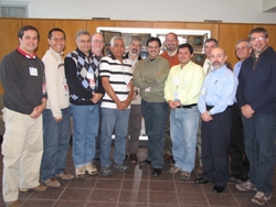
10 Mexican professors and 3 Sandia researchers at a SUMMit design course for MEMS devices held at Sandia in December 2009. Ernest Garcia is third from right. (Photo courtesy of Universidad Autonoma de Ciudad Juarez)

The rationale for the agreement is that the economic well-being of Mexico is a national security issue for the United States, said Sandia project lead Ernest Garcia.

Sandia’s SUMMiT V fabrication process will permit students to design MEMS devices that employ five layers of silicon. Each layer adds another level of complexity to the design. SUMMiT V permits advanced systems created on moveable platforms to be taller (up to 12 micrometers high), stiffer, and more mechanically forceful and robust than those created by earlier processes.

"The University of Guadalajara is like the state of California’s higher education system," Garcia said. "It supports a number of universities throughout the Mexican state of Jalisco. Its leadership wants to use SUMMiT as the basis for a future graduate program in MEMS."

"MEMS manufacturing will leverage many of Mexico’s traditional strengths in electronic manufacturing," Herrera said. "Sandia is in a position to help the University of Guadalajara system migrate to a state-of-the-art MEMS design capability."

"If we could help Mexico improve its research and development capabilities, it would help stabilize its economy," he said. Garcia sees the new collaboration with the U. of Guadalajara as a long-term investment in the future of the Mexican economy. "It’s not a sprint, it’s a marathon," Garcia said, mentioning potential barriers like U.S. controls on exporting technology and intellectual property (IP) to foreign countries.
Click to Enlarge
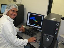
A student in a clean room at the Universidad Autonoma de Ciudad Juarez, which has an ongoing arrangment with Sandia National Labs. Sandia’s MOU with the U. of Guadalajara will open MEMS education to more Mexican students. (Photo courtesy of Universidad Autonoma de Ciudad Juarez)

"Ultimately, the U.S. may be the biggest beneficiary if the MOU contributes to the vitality of the Mexican economy and thereby the stability of the U.S.-Mexican border," said Gil Herrera, director of Sandia’s Microsystems Science, Technology and Components Center. "We believe that Sandia will also benefit from the relationship, as we will have new minds challenging the design envelope of our SUMMiT MEMS technology." Herrera is in charge of Sandia’s activities in support of the collaboration.

Steve Rottler, Sandia’s vice president for basic technologies, signed the agreement for Sandia. He said, "The commitment and enthusiasm of the University of Guadalajara faculty and leadership will greatly help this collaboration to advance technologies vital to the economies and security of both countries."

Similar efforts by Sandia are also underway at Mexican universities in Juarez, Veracruz and Mexico City, as well as the Puebla-based National Institute of Astrophysics, Optics, and Electronics (INAOE).

The agreement extends earlier work by Sandia that played a role in creating a Bi-National Sustainability Laboratory at Santa Teresa, NM, near the border between the United States and Mexico. That effort was intended to examine problems on both sides of the border, such as water rights. The initial goal of the Sustainability Laboratory was to foster research efforts that could ultimately create border industries and jobs to staunch the one-way flow of workers from Mexico to the United States. That effort is now directed by an independent nonprofit corporation supported by a variety of national, state, and corporate sponsors.

The Guadalajara program is expected to expand an existing Sandia-led national MEMS project for Mexico. That country has spent $2 million to fund the project. "Last December, a number of Mexican professors took our MEMS course, licensed our design software, and purchased 100 silicon chips with their MEMS designs," Garcia said.

The Guadalajara agreement is different, Garcia said, because it (and Sandia efforts with other Mexican universities) are in the interior of Mexico rather than near the border.

"We hope eventually to have Mexican universities compete in Sandia’s University Alliance annual MEMS competition for the most imaginative or practical designs," Garcia said. The high-spirited contest, open to institutional members of the Sandia-led MEMS University Alliance program, provides an arena for student engineers to hone their skills in designing and using microdevices. Student contest winners get to see their designs become reality when they are fabricated at Sandia’s MEMS facilities.  Last year’s winners were Texas Tech and the University of Utah for creating, respectively, the world’s smallest chess set and a micro barber shop that serviced  a single human hair.

A delegation of Mexican professors from Guadalajara will visit Albuquerque in spring 2011 to confer with researchers at Sandia and possibly the University of New Mexico. The trips will be funded by state of Jalisco’s technology office. Albuquerque and Guadalajara are sister cities.

Sandia National Laboratories is a multiprogram laboratory operated and managed by Sandia Corporation, a wholly owned subsidiary of Lockheed Martin Corporation, for the U.S. Department of Energy’s National Nuclear Security Administration. With main facilities in Albuquerque, N.M., and Livermore, Calif., Sandia has major R&D responsibilities in national security, energy and environmental technologies, and economic competitiveness. Learn more at www.sandia.gov

Follow Small Times on Twitter.com by clicking www.twitter.com/smalltimes. Or join our Facebook group