Tag Archives: Small Times Magazine

February 2, 2011 — Sun-drenched roofs, windows, deserts and even clothing will someday be integrated with inexpensive solar cells that are many times thinner and lighter than current options. It is not hard to envision a time when integrated solar technologies will be ubiquitous in our increasingly energy-hungry lives. A multidisciplinary team of Stanford engineers led by Mike McGehee, Yi Cui and Mark Brongersma, and joined by Michael Graetzel at the École Polytechnique Fédérale de Lausanne (EPFL), are focused on that goal.

The Stanford/EPFL team succeeded in harnessing plasmonics to more effectively trap light within thin solar cells to improve performance and production feasability. Results were published in Advance Energy Materials.

"Plasmonics makes it much easier to improve the efficiency of solar cells," said McGehee, an associate professor of materials science and engineering at Stanford, and director of CAMP, Center for Advanced Molecular Photovoltaics, a multidisciplinary, multi-university team tackling the challenges of thin-film solar cells.

"Using plasmonics we can absorb the light in thinner films than ever before," McGehee said. "The thinner the film, the closer the charged particles are to the electrodes. In essence, more electrons can make it to the electrode to become electricity."

 Click to Enlarge
Figure 1. Acting like a waffle iron, silicon nanodomes, each about 300 nanometers in diameter and 200 nanometers tall, imprint a honeycomb pattern of nanoscale dimples into a layer of metal within the solar cell. Image courtesy of Michael McGehee.

Plasmonics is the study of the interaction of light and metal. Under precise circumstances, these interactions create a flow of high-frequency, dense electrical waves rather than electron particles. The electronic pulse travels in extremely fast waves of greater and lesser density, like sound through the air.

To make the plasmonic dye-sensitized solar cell (DSSC), the team imprinted a honeycomb pattern of nanoscale dimples into a layer of metal within the solar cell, like a nanoscale waffle, with the bumps on the waffle iron as domes rather than cubes. McGehee and team members spread a thin layer of "batter" on a transparent, electrically conductive base. This batter is mostly titania, a semiporous metal that is also transparent to light. Next, they use their nano waffle iron to imprint the dimples into the batter. They then layer on a light-sensitive dye that oozes into the dimples and pores of the substrate. Lastly, the engineers add a layer of silver, which hardens almost immediately.

Click to Enlarge
Figure 2. Titania within the solar cell is imprinted by the silicon nanodomes like a waffle imprinted by the iron. Image courtesy of Michael McGehee.

When all those nanodimples fill up, the result is a pattern of nanodomes on the light-ward side of the silver. This bumpy layer of silver has two primary benefits. First, it acts as a mirror, scattering unabsorbed light back into the dye for another shot at collection. Second, the light interacts with the silver nanodomes to produce plasmonic effects. Those domes of silver are crucial. Reflectors without them will not produce the desired effect. Nanodomes must be precisely the right diameter, height, and spacing to fully optimize the plasmonics. Read more about nanotechnology here.

Photons enter and pass through the transparent base and the titania, at which point some photons would be absorbed by the light-sensitive dye, creating an electric current. Most of the remaining photons would hit the silver back reflector and bounce back into the solar cell. A certain portion of the photons that reach the silver, however, will strike the nanodomes and cause plasmonic waves to course outward.

Dye solar cells typically reach 8% efficiency and 7 year life spans — significantly below photovoltaic industry standard of 25% efficiency, 20-30 year lifetime. Engineers like McGehee believe that if they can convert just 15% of the light into electricity and extend the product lifecycle to a decade, the roll-to-roll production, less toxic materials, flexibility, light weight, and other benefits of this emerging thin-film tech will outweigh the lower numbers.

Learn more at http://www.stanford.edu/

Courtesy of Andrew Myers, associate communications director for the School of Engineering, Stanford.

Also read: EU partners eye metallic nanostructures for solar cells 

Subscribe to Photovoltaics World

Follow Photovoltaics World on Twitter.com via editors Pete Singer, twitter.com/PetesTweetsPW and Debra Vogler, twitter.com/dvogler_PV_semi.

Or join our Facebook group

February 1, 2011 — Coventor, design technology supplier for micro-electromechanical systems (MEMS), and the nanoelectronics research center imec formed a strategic partnership to improve and expand the use of advanced design and manufacturing techniques for the development of CMOS-integrated MEMS. The partnership includes strategic alignment on R&D roadmaps and collaboration on advanced research topics. Teams of imec and Coventor will collaborate on expanding imec’s use of Coventor’s software tools suite for MEMS + IC design. They will jointly develop process design kits (PDKs) for imec’s SiGe MEMS-above-IC process.

Building on both organizations’ success with MEMS design and manufacturing, the partnership aims to make MEMS more accessible to MEMS and IC designers. PDKs will be developed to improve the efficiency of MEMS-IC co-design. The kits will target imec’s SiGe MEMS technology that uses a MEMS-last approach, where the MEMS are processed after and on top of the CMOS circuits, enabling a monolithic integration of MEMS devices with the driving and readout electronics on the same die. The SiGe MEMS platform’s flexible and modular approach also allows application-specific tuning and optimization of MEMS layer thicknesses and properties, and the processing of optional functional layers on top of the MEMS devices.

The partnership will leverage Coventor’s background in developing the necessary infrastructure for MEMS design environments. Coventor’s design tools have been production proven on hundreds of MEMS designs over the past 15 years. Recently, Coventor introduced a new product line, MEMS+, aimed at integrating MEMS design with mainstream IC design environments.

"Product developers from a wide range of industries look to integrate MEMS because of their powerful capabilities. Imec is well-positioned to address this market through its CMORE initiative, which seeks to expand the scaling of CMOS micro- and nano-devices by adding functions other than logic and memory to chips," said Rudi Cartuyvels, VP process technology at imec. Also read: Two different approaches to integrated MEMS by Dick James, Chipworks

"Coventor’s strategy revolves around the ‘democratization’ of MEMS, which is about eliminating the obstacles and challenges in the way of more widespread adoption of these devices. [With imec,] we can develop more efficient and practical approaches to MEMS development that meet the demanding requirements of markets and applications that have yet to leverage the vast potential of MEMS,” said Mike Jamiolkowski, CEO of Coventor.

Imec performs world-leading research in nanoelectronics. Further information on imec can be found at www.imec.be.

Coventor Inc. provides automated design solutions for micro-electromechanical systems (MEMS). More information is available at http://www.coventor.com 

Follow Small Times on Twitter.com by clicking www.twitter.com/smalltimes. Or join our Facebook group

February 1, 2011 — Leica Microsystems and Digital Surf announced an agreement whereby Leica Map surface imaging and metrology software, based on Digital Surf’s Mountains Technology, will be used with the Leica Application Suite (LAS) for Leica industrial microscopes. The Leica Map software is used to visualize and quantify features of measured surfaces, characterize surface texture and geometry, and generate visual surface metrology reports with full traceability. It is available on three levels with optional modules for advanced applications.

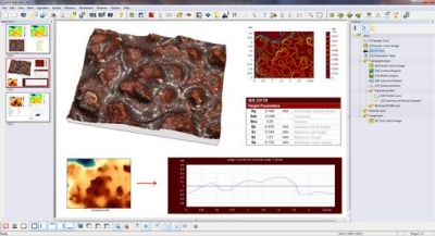
Click to EnlargeEntry-level Leica Map Start software is used in conjunction with LAS Montage. LAS Montage acquires a series of image planes at known spacing covering the in-focus region of a specimen with a Leica microscope. From this stack a depth map and an extended focus image are derived and analyzed by Leica Map. In Leica Map Start, surface topography can be viewed at any zoom level and any angle in real time. Color and intensity image overlays facilitate the location of surface features, including defects. Distances, angles, and step heights can be measured. Height and functional parameters are calculated in accordance with the latest ISO 25178 standard on areal surface texture. Optional modules can extend the capability to surface texture and contour analysis.

Leica Map DCM 3D software is dedicated to the Leica dual core 3D microscope Leica DCM 3D, which combines confocal and interferometry technology for non-invasive, high speed, and high-resolution assessment of micro and nano structures. In addition to the standard features of Leica Map Start, Leica Map DCM 3D includes advanced ISO 16610 filtering techniques for separating surface roughness and waviness, basic functional analysis (bearing ratio, depth distribution, etc.), and the ability to extract sub-surfaces (for example from mechanical and electronic components and MEMS) and analyze them independently.

Leica Map Premium is a top of the line universal solution that is compatible with single-point tactile and optical profilometers and scanning probe microscopes, as well as with optical microscopes.

"Leica Map software is based on the latest generation of Mountains Technology, which was released in the second half of 2010," stated François Blateyron, COO of Digital Surf. "It incorporates an enhanced desktop publishing environment, to speed up complex calculations and the processing of large measurement data sets."

Leica Microsystems provides microscopes and scientific instruments. Leica Microsystems is organized in four divisions: the Life Science Division, Industry Division, Biosystems Division and Medical Division.

Digital Surf provides imaging and analysis software for surface metrology instruments including confocal microscopes, optical interferometric microscopes, scanning probe microscopes and 2D/3D profilometers.

Follow Small Times on Twitter.com by clicking www.twitter.com/smalltimes. Or join our Facebook group

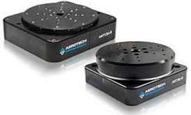
February 1, 2011 — Aerotech ANT95-R and ANT130-R direct-drive rotary stages, part of Aerotech’s nano Motion Technology product line, offer in-position stability of 0.005 arc sec and incremental motion of 0.01 arc sec using the company’s direct-drive technology. They suit demanding high-throughput manufacturing applications such as disk-drive and MEMS manufacture and test, fiber-optic device alignment, as well as super-high-precision laboratory R&D applications.

Click to EnlargeThe ANT95-R and ANT130-R rotary stages are available in 20°, 180°, or 360° continuous travel. Maximum speed is 200rpm and maximum acceleration is 400rad/s2. Axial load capacity is 2kg for the ANT95-R and 3kg for the ANT130-R. These rotary stages also offer an 11mm clear aperture that can be used for product feed-through, laser beam delivery, cable clearance, or application-specific requirements.

The ANT95-R and ANT130-R series are designed for compatibility and easy integration with Aerotech’s ANT linear stages. Together these stages provide the accuracy, stability, and performance required for current and future nano-manufacturing and inspection applications. Their low profile reduces the effective working height, minimizing "stack-up" related errors when used as part of a multi-axis system.

The ANT95-R and ANT130-R were designed to operate in a 24/7 manufacturing environment while providing laboratory-grade accuracy. Unlike other extremely precise rotary devices, they require no periodic maintenance, and direct-drive technology ensures years of trouble-free operation.

Aerotech offers a complete motion system solution to get the most from your ANT series stage. Motion control options include the software-only 1-32 axis Automation 3200 machine controller, the stand-alone 1-10 axis Ensemble series motion controller, and the stand-alone single-axis Soloist series. Both PWM and ultra-low-noise linear amplifiers are available to complete your Aerotech motion system. Learn more at http://www.aerotech.com/

Follow Small Times on Twitter.com by clicking www.twitter.com/smalltimes. Or join our Facebook group

February 1, 2011 — King Abdulaziz City of Science and Technology (KACST) signed an agreement with imec to host researchers from KACST-INTEL consortium Center of Excellence in Nano-manufacturing Applications (CENA) at imec facilities in Belgium starting September 2011, for a period of three years. CENA focuses on leading-edge research on advanced nano-processing and fabrication technology, and aims at supporting the growth of Saudi Arabia’s knowledge-based economy and at boosting its competitiveness on both regional and international levels.

Commenting after signing the agreement, H.E. Dr. Mohammed Ibrahim Al-Suwaiyel, president of KACST said, "Imec is a world-leading research center, which provides an environment that will enrich the experience of CENA students/researchers and offer significant and relevant experience in applied nanotechnology research." Dr. Al-Suwaiyel further emphasized CENA’s role in fostering collaboration between KACST as the leading research establishment in the Kingdom of Saudi Arabia, Intel Corporation and academic institutions across the Arab World and Turkey.

Dr. Luc Van den hove, president and CEO of imec, praised the agreement as the first collaboration opportunity between KACST and imec and added: "We are pleased about the CENA hosting arrangement and are committed to continue to explore with KACST collaborations in other research areas relevant to both organizations."

H.H. Prince Dr. Turki S. Al-Saud, KACST VP for research institutes, said: "The focus of CENA is to conduct leading-edge research on advanced nano-processing and fabrication technology, including MEMS/NEMS, nano-sensors and networks, nano-devices, and synthesis and deposition of nano-structures." H.H. Dr. Turki Al-Saud pointed out: "Establishing CENA is considered an important step reflective of KACST’s effort, in particular, and the Kingdom of Saudi Arabia, in general, in enhancing graduate education, promoting advanced technology research and creating an environment of innovation for researchers in the Kingdom and Arab world & Turkey."

"The choice of imec reflects the close relationship between Intel and imec that spans more than two decades covering various areas of research in the field of semiconductor processing and advanced lithography," said Dr. Makarem Hussein, CENA director. "This hosting agreement further underscores KACST continued effort in building the human resources needed for strong nanotech research in the Kingdom of Saudi Arabia. It is also a step towards making reality its vision for turning Saudi Arabia into a regional hub for science and research;" added Dr. Hussein.

CENA is planning the launch of "CENA DAY" events during March 2011 to engage imec researchers with eligible students and researchers in the region. Scholarships will be granted to selected students pursuing doctorate and master degree in various disciplines of engineering and science who are registered at universities affiliated with CENA through a joint research and academic advising agreement with CENA in the Kingdom of Saudi Arabia and throughout the Arab world and Turkey.

Imec performs world-leading research in nanoelectronics. Further information on imec can be found at www.imec.be.

King Abdulaziz City for Science and Technology (KACST) is an independent scientific organization administratively reporting to the Prime Minister of Saudi Arabia. KACST is both the Saudi Arabian national science agency and its national laboratories. The science agency function involves science and technology policy making, data collection, funding of external research, and services such as the patent office.

Intel (NASDAQ: INTC) designs and builds the essential technologies that serve as the foundation for computing devices. Additional information about Intel is available at www.intel.com.

Follow Small Times on Twitter.com by clicking www.twitter.com/smalltimes. Or join our Facebook group

January 31, 2011 — Researchers at Imec proposed a portable, lab-on-a-chip system for single nucleotide polymorphism (SNP) detection in DNA at IEEE’s International Electron Devices Meeting (IEDM, 12/6-12/8/10, San Francisco, CA; paper #36.3, "Design and fabrication of a biomedical lab-on-chip system for SNP detection in DNA"). The research has implications for personalized medicine, enabling doctors to travel to patients in their homes to personalize/customize their medical treatments.

Maaike Op de Beeck, program manager Human++, Heterogeneous Integrated Microsystems Department, at Imec, met with Debra Vogler, senior technical editor, at IEDM and provided background on the research in a podcast interview.

Listen to Op de Beeck’s interview: Download (for iPhone/iPod users) or Play Now

"We all have DNA of course, but sometimes there are errors in its duplication," said Op de Beeck. "When there is an error in just one single base pair, we call it an SNP." Often SNPs have no consequence; however, sometimes they do, explains Op de Beeck. And they result in differences between people, with some SNPs being an indication of a predisposition for certain diseases. This information can be used by doctors to identify personalized/optimized treatment of diseases during home visits, or even possibly in nursing homes. Hospitals typically use larger table-top tools for fluid manipulation during such a procedure, Op de Beeck tells ElectroIQ, but they might also be interested in the smaller, faster, and portable aspects of the lab-on-chip device, she suggests.

A key component of the lab-on-chip device is a Si-based micro-pillar filter that enables separation of DNA segments with different length. An on-chip integrated conductive polymer actuator generates the high pressure required to sustain the fluid flow through the system.

Subscribe to Solid State Technology/Advanced Packaging.

Follow Solid State Technology on Twitter.com via editors Pete Singer, twitter.com/PetesTweetsPW and Debra Vogler, twitter.com/dvogler_PV_semi.
Or join our Facebook group

January 31, 2011 — Researchers from Boston College (BC), MIT, Clemson University and the University of Virginia have used nanotechnology to achieve a 60-90% increase in the thermoelectric figure of merit of p-type half-Heusler, a common bulk semiconductor compound, the team reported in the journal Nano Letters.

The dramatic increase in the figure of merit, used to measure a material’s relative thermoelectric performance, could pave the way for a new generation of products — from car exhaust systems and power plants to solar power technology — that that runs cleaner, according to co-author Xiao Yan, a researcher in the Department of Physics at Boston College.

The team registered improvement in half-Heusler, which has been under study for its thermal stability, mechanical sturdiness, non-toxicity, and low cost. However, the application of half-Heusler has been limited because of its poor thermoelectric performance: it previously registered a peak figure of merit of approximately 0.5 at 700 oC for bulk ingots.

Yan, working with BC Professor of Physics Zhifeng Ren and MIT’s Soderberg Professor of Power Engineering Gang Chen, have increased the figure of merit value of p-type half-Heusler to 0.8 at 700 oC. Moreover, the groups’ material preparation methods proved to save time and expense compared with conventional methods.

"This method is low cost and can be scaled for mass production," Ren said. "This represents an exciting opportunity to improve the performance of thermoelectric materials in a cost-effective manner."

The researchers obtained their results by first forming alloyed ingots using arc melting technique and then creating nanoscale powders by ball milling the ingots and finally obtaining dense bulk by hot pressing. Transport property measurements together with microstructure studies on the nanostructured samples, in comparison with that of bulk ingots, showed that the thermoelectric performance improves largely because of low thermal conductivity produced by enhanced phonon scattering at grain boundaries and defects in the material. The material was also found to have a high Seebeck coefficient, a measure of thermoelectric power.

Researchers in the BC and MIT labs are still trying to prevent grain growth during press, which accounts for the still large thermal conductivity of half-Heusler.

"Even lower thermal conductivity and improved thermoelectric performance can be expected when average grain sizes are made smaller than 100nm," said Ren, who was joined on the team by fellow Boston College researchers Giri Joshi, Weishu Liu, Yucheng Lan and Hui Wang, MIT’s Sangyeop Lee, Virginia’s Rogers Professor of Physics Joe Poons and J.W. Simonson and Clemson Professor of Physics Terry M. Tritt.

Learn more at www.bc.edu.

Follow Small Times on Twitter.com by clicking www.twitter.com/smalltimes. Or join our Facebook group

January 28, 2011 – BUSINESS WIRE — Vistec Lithography Inc. received an order from Turkey for one of its electron-beam lithography systems. An EBPG5000plusES will be delivered to the newly formed Nanotechnology and Application Center (SUNAC) of the Sabanci University based in Istanbul. The Gaussian Beam system fulfills the challenging requirements of the institute which will collaborate in the field of nanotechnology research with other institutions.

Click to Enlarge"The EBPG5000plusES is a 100kV high-performance system…It will enable us to address the nanotechnology development needs of natural sciences, applied sciences and engineering programs," says Dr. Volkan Özgüz, director of the Nanotechnology and Application Center.
Vistec’s EBPG5000plusES are dedicated electron-beam lithography systems developed to meet the diverse requirements for advanced nano-lithography applications in direct write for both R&D and production of GaAs devices. It enables a rapid exposure with a 25MHz rate and a minimum feature size of less than 8nm. The EBPG5000plusES system is capable to expose various substrate types including masks and dimensions up to 150mm size.

Vistec is pleased to have received its first order from a Turkish university. "Due to their flexibility and the multi user environment, our systems are a perfect match to the needs of universities or industry research institutions. After selling a number electron-beam lithography systems to international well-known institutes in the last year, we are highly motivated to continue this positive development in the upcoming year," says Rainer Schmid, GM at Vistec Lithography Inc.

Sabanci University is a private university with a state of the art campus spread over 1,260,000 m2 and located 40 km from Istanbul’s city center, in Turkey. It has the distinction of being the first university in Turkey accepted for membership in the European Foundation for Quality Management (EFQM). www.sabanciuniv.edu

The Vistec Electron Beam Lithography Group is a global manufacturer and supplier of electron-beam lithography systems with applications ranging from nano and bio-technology to photonics and industrial environments like mask making or direct writing for fast prototype development and design evaluation. The Vistec Electron Beam Lithography Group combines Vistec Lithography and Vistec Electron Beam. www.vistec-semi.com

Vistec Lithography develops, manufactures, and sells electron-beam lithography equipment based on Gaussian Beam technology. Vistec Electron Beam is providing electron-beam lithography equipment based on Shaped Beam technology.

Follow Small Times on Twitter.com by clicking www.twitter.com/smalltimes. Or join our Facebook group

January 27, 2011Microvisk Technologies, developer of a handheld system to monitor the blood clotting status of patients taking the drug Warfarin, raised £6 million (US $9.54 million) through a rights issue to existing investors in an oversubscribed round. This is the third round of funding for Microvisk, which has secured £10.5 million in the past 12 months.

The round included investment from Porton Capital, Oxford Technology Management, New Hill (Boston, MA), Midven, the Rainbow Seed Fund, Finance Wales, and private investors. Previous rounds in 2010 saw Microvisk attract £4.5 million from new and existing investors.

A spin-out company from the Science and Technology Facilities Council, Microvisk has developed a medical diagnostic strip based on a micro-electro-mechanical system (MEMS) that was created as a movement system for nano-robots. The Microvisk product is a solid state system that requires far less blood for the Prothrombin or INR test than conventional systems. The "SmartStrip" is a disposable strip that uses embedded sensors to work out the clotting speed of blood from a finger prick sample and the results are displayed on a handheld reader. The coagulation status (clotting speed) of the patient is measured by tiny multi-layered paddles on the surface of the strip (a small cantilever measures viscosity) and a memory chip enures the device is calibrated for accuracy.

Microvisk will launch the Smartstrip device in the UK market in Fall 2011, and starting trials in the US and Germany within the next 6 months. Microvisk will launch the Smartstrip in these countries in 2012. The capital raised via the funding round to continue clinical trials in the UK and expand its research and manufacturing facilities as well as recruiting additional scientists and manufacturing staff.

Warfarin is used by 7 million people in the western world, with over 1 million new patients annually (according to FDA estimates cited by Microvisk). Patients must have regular blood tests to monitor dosage. Blood clots can form if doses are too low; bleeding can result from too-high doses. Smartstrips allow patients to test blood coagulation at home, as opposed to hospital or doctor visits, enabling at-home healthcare.

Microvisk is a UK-based company developing medical testing devices based on MEMS for the international medical market. Learn more at www.microvisk.com

Also read: A new take on MEMS innovation by Marlene Bourne

Follow Small Times on Twitter.com by clicking www.twitter.com/smalltimes. Or join our Facebook group

January 27, 2011 — McPherson’s high-resolution spectrometer, Model 2061, is now available for scanning and imaging applications via 2D CCD or CMOS detectors. It suits emission, luminescence, Raman (strained Silicon), and high-temperature plasma measurement with better than 0.02nm full width half maximum spectra.

Click to Enlarge

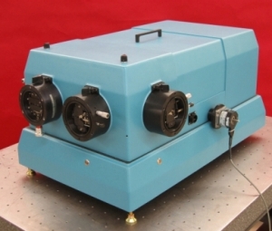
The 1m focal length spectrometer features bilaterally adjustable slits, multiple entrance and exit port locations, and high precision wavelength drive for reproducibility. The capability to mount large, high-angle Echelle type diffraction gratings is built in. The 50mm-wide focal plane is readily accessible.

Oversized McPherson Snap-In gratings fitting the 1m Model 2061 are easily interchangeable and provide 40% more diffractive ruled area. Matching, focusing and collimating optics provide excellent light throughput and operation with f/7 aperture. Many diffraction gratings are available to tailor systems for a wide-spectral range or desired spectral resolution. Spectral resolution with a 10µm entrance slit and a 1200g/mm grating is better than 0.02nm full width half maximum.

McPherson Inc. manufactures instruments that measure and tune specific wavelengths of light for many disciplines of spectroscopy. Learn more at www.McPhersonInc.com

Follow Small Times on Twitter.com by clicking www.twitter.com/smalltimes. Or join our Facebook group