Tag Archives: Small Times Magazine

January 21, 2011 – JCN Newswire — Professor Kohei Itoh, who is developing quantum computers based on silicon semiconductors at Keio University’s Faculty of Science and Technology, together with Dr. John Morton at Oxford University and others, successfully generated and detected quantum entanglement between electron spin and nuclear spin in phosphorus impurities added to silicon. This accomplishment constitutes a major breakthrough toward the achievement of quantum computers.

"According to Moore’s Law, which serves as the index for semiconductor microfabrication, by 2030, individual atoms in silicon will be used for computing," commented Professor Itoh. "The question of whether that kind of computing is possible was the starting point for my research, and as a way of approaching that question, I began to research computing using atoms in silicon. Now, we’ve performed the first successful experiment on computing using phosphorus atoms in silicon, and been able to create a special state called quantum entanglement. I am glad that this research has led to a world-first result: computing using atoms in silicon, the most important semiconductor."

The results of this research were featured in the British science journal Nature (online edition) on January 19, 2011.

Quantum computers work using entirely different principles from current computers, enabling new characteristics. Quantum superposition and entanglement drive the technology. Classical computers can only use states corresponding to one or other of the binary digits 0 and 1. By contrast, quantum bits, the minimum units for quantum computers, consist of individual quanta, in the form of atoms, electrons, and photons, and can represent 0 and 1 at the same time (superposition state). Another prerequisite for quantum computers is entanglement between at least two quantum bits. In an entangled state, individual quantum bits are entangled in a way that transcends space, so they cannot be separated and treated as 0 or 1.
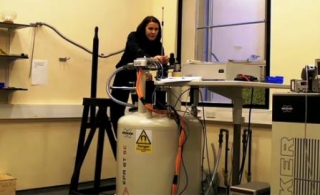
Click to EnlargeThis joint research by Keio University and Oxford University has achieved the first successful production and detection of entanglement in silicon. Phosphorus impurities are added to silicon to produce n-type silicon. Phosphorus atoms in silicon at low temperatures, less than 20K, capture an electron and behave like hydrogen atoms. Using this characteristics, the joint research group has produced and detected entanglement between two quantum bits by treating the nuclear spin of a phosphorus atom as one quantum bit and the captured electron’s spin as another quantum bit. The entanglement was produced at once for each of a large number of phosphorus impurities that exist in the sample in the order of 10 to the power of 10. The process of generating entanglement itself is equivalent to quantum computing.

Previously, coherence of quantum bits in silicon was too short. In ordinary silicon, the quantum information in phosphorus impurities is lost before entanglement is generated and measured. Keio University made coherence sufficiently long by ensuring that all the atoms in the silicon were the isotope 28Si, while a special magnetic resonance (MR) apparatus belonging to Oxford University produced a field of 3.4 Tesla at a temperature below 3K, to obtain high polarization of electron spin and nuclear spin in phosphorus.

In response to the question "What is a state-of-the-art quantum computer?", the usual example cited is a nuclear magnetic resonance (NMR) result with seven quantum bits, where the prime factorization 15 = 3 x 5 was performed successfully [L. Vanersypen, et al., Nature Vol. 414, 883 (2001)]. However, in the NMR research, the same number of calculation steps as in a classical computer was required to make it seem as if seven quantum bits in molecules were aligned, and entanglement was not obtained. By contrast, in this research, by using a low temperature and high magnetic field, and careful arrangements for quantum computing, quantum bits were initialized in a very small number of steps, and entanglement was successfully generated and detected. The entanglement state found in a large number of phosphorus atoms added to silicon constitutes a major breakthrough toward a solid-state quantum computer.

This research was conducted as part of "Quantum spintronics based on donor impurities in isotope-controlled silicon" (research representative in Japan: Prof. Kohei Ito; research representative in the UK: Dr. John Morton), a project in the JST’s "Strategic International Cooperative Program" with the UK’s EPSRC.

Entanglement can be explained with the example of two spatially separated quanta, in London and Tokyo. Suppose that, in both Tokyo and London, a quantum bit is in a superposition state, where its value is both 0 and 1. If the state is determined from before it is measured, but not known until it is measured, the bit is in a classical state, not a quantum state. In a quantum state, before the quantum bit is measured, its state is both 0 and 1, but the instant the state is measured, it becomes a classical state of 0 or 1. Measuring the quantum bit turns it into a classical bit. A case where there is a correlation between the bits, so if the quantum bit in Tokyo is measured and the value 0 is obtained, the quantum bit in London must be 1, and if the Tokyo bit is 1, the London bit must be 0. This is also called entanglement, as the two bits cannot be separated. Even though each of the bits, in Tokyo and London, has a state that is both 0 and 1, the instant the bit in Tokyo is measured and takes the classical state 1, it is determined that the London bit has the value 0. This correlation, which transcends space, exemplifies the mysterious nature of quantum mechanics, which cannot be explained using classical mechanics.

Keio is Japan’s first private institution of higher learning.

Japan Science and Technology Agency (JST) is an integrated organization of science and technology in Japan that establishes an infrastructure for an entire process.

Subscribe to Solid State Technology/Advanced Packaging.

Follow Solid State Technology on Twitter.com via editors Pete Singer, twitter.com/PetesTweetsPW and Debra Vogler, twitter.com/dvogler_PV_semi.

Or join our Facebook group

January 20, 2011 — The Power Sources Manufacturers Association (PSMA) Nanotechnology Committee is sponsoring a Special Presentation session at APEC 2011 titled "Nanotechnology: Enabling the Next Generation of Power Electronics."

The session will take place on Thursday morning, March 10th, 2011 at the Fort Worth Convention Center in Fort Worth, Texas and will provide a broad overview of current nanotechnology applications, materials and opportunities.

Featured are six invited experts from industry, research and government who will provide attendees an overview of the current applications and insights that may enable them to anticipate and identify potential opportunities for their companies to participate in markets with this emerging technology. Nanotechnology is already being applied in semiconductors, components, packaging and power storage designs.

According to Gerald Castellucci, National Institute of Standards and Technology, and Ernie Parker, Crane Aerospace & Electronics, co-chairs of the session, "This Special Presentation session will not only be very informative but will also provide an opportunity for attendees to interact with other professionals who are active in the evolving application of nanotechnology in materials and designs. We encourage people to register for APEC 2011 and make plans to attend the Special Presentation Session and to consider participating in the other PSMA-sponsored meetings during the week."

A non-profit professional organization, PSMA was founded to enhance the stature, reputation and products of its member organizations, while also improving their knowledge of existing and emerging power source technologies and their application. PSMA’s stated aim is to educate the entire electronics industry, academia, government and industry agencies on the importance of power-source and conversion devices to the continued development and advancement of power electronics systems for the betterment of all.

Follow Small Times on Twitter.com by clicking www.twitter.com/smalltimes. Or join our Facebook group

January 20, 2011 – BUSINESS WIRE — The Center for Micro/Nano Science and Technology at National Cheng Kung University (NCKU), Tainan, Taiwan, has moved from Building of Science and Technology, Tzu-Chiang Campus, to the Building for Instrumentation Equipments, which occupies more than 600 square meters and includes cleanrooms and laboratories.

Under the leadership of director Jen-Fin Lin and with the joint efforts of staff, the NCKU Center for Micro/Nano Science and Technology has constructed and moved more than 10 valuable equipments within three months, reduced the transportation cost to NT$500,000, and recovered all the equipments to order within one month.

Subsidized by the Taiwan National Science and Technology Program for Nanoscience and Nanotechnology and Research University Integration Project from the Ministry of Education, the Center is a key institute for nano technology and research in Southern Taiwan with more than sixty valuable instruments. NCKU Center for Micro/Nano Science and Technology, established in 1997, was NSC MEMS Southern Common Facility Center and was renamed as Center for Micro/Nano Science and Technology in 2002.

To strengthen the sustainable development of the Center for Micro/Nano Science and Technology, additional key instruments are necessary, and as the number of instruments increases, space in the Building of Science and Technology became limited, inadequate to use, and difficult to maintain. In addition, nearby residents have complained about the issues of exhaust and noise, thus the university decided to move the Center to Building for Instrumentation Equipments to a new home. 

NCKU president Michael Ming-Chiao Lai said, "After the Center for Micro/Nano Science and Technology moves into Building for Instrumentation Equipments, I believe the comfortable and spacious room can offer better service to students, teachers and the industry and the brand-new clean rooms and laboratories can provide complete space for micro nanometer manufacturing and testing equipments." Ming-Chiao Lai believed that the newly migrated Center for Micro/Nano Science and Technology will help promote academic exchange and industry-academia cooperation.

Nano science is an advanced technology which covers different fields, including electrical engineering, medicine and materials, and to engage in cross-disciplinary cooperation, excellent equipments are needed to attract scientists from different fields to work together and learn from one another.

NCKU senior executive VP Hwung-Hweng Hwung emphasized, "A person who engages in research requires excellent research equipments. From my personal experience, with a set of laser tester I purchased in 1981, my papers published in international journals have never been rejected and many of them have been cited. Because I have such excellent equipments in Tainan Hydraulics Laboratory, I could measure the most sophisticated data and come up a precise analysis." Hwung believes, for a research center to develop sustainably, it must have equipments, instruments and personnel like those of Tainan Hydraulics Laboratory, and the Director of the Center must use these equipments to create new projects.

He added, "To become a national-scale research center, the Center must not rely entirely on university resources or government long-term budget, thus I expect the Director to pay extra attention to this aspect."

The core instruments of NCKU Center for Micro/Nano Science and Technology include E-beam Writer, Ultra-High Vacuum Ion Beam Sputter, High Quality Sputtering and Evaporation System, Dual-Beam Focused Ion Beam, High-Resolution Field-Emission Transmission Electron Microscopy and Mask Aligner.

Learn more about National Cheng Kung University at www.ncku.edu.tw

Follow Small Times on Twitter.com by clicking www.twitter.com/smalltimes. Or join our Facebook group

January 20, 2011 – PRNewswireSTMicroelectronics (NYSE: STM), micro-electro-mechanical systems (MEMS) devices supplier to consumer and portable applications, and Bluechiip Limited, an early-stage company that has developed a tracking solution, will cooperate in the manufacturing of MEMS-based tracking tags, aimed initially at healthcare applications, such as biobanks.

As the bluechiip tracking tag is a mechanical device, it can survive and read sample IDs in extremely high and low temperatures, in addition to its immunity to gamma irradiation. This robustness provides significant advantages over more traditional identification or tracking solutions, such as labels, barcodes or RFID technologies, and provides the necessary high levels of data surety in the rapidly growing and labor-intensive healthcare markets, especially in biobanking.

This new technology enables data to be read at temperatures as low as those reached in liquid nitrogen, approximately –196C, and as high as 200C. Data can also be transmitted through frost. Bluechiip’s tracking solution has also been field-proven to survive autoclaving, gamma irradiation sterilization, humidification, centrifuging, cryogenic storage and frosting.

The technology is based on MEMS-based resonators within a tiny, purely mechanical chip, containing no electronics. The tracking tag, which comprises this mechanical chip and an antenna, can either be embedded or manufactured into a storage product, such as a vial or a bag. Easy identification, along with any associated information from the tag can be detected by a reader, which can also log the temperature history of the tagged items.

"Bluechiip’s tag technology coupled with ST’s MEMS design and manufacturing expertise will make available an extremely robust and valuable tracking capability for many applications in healthcare and other markets," said Benedetto Vigna, Group Vice President and General Manager, MEMS, Sensor and High-Performance Analog Division, STMicroelectronics. "ST has a long history in the industrialization of innovative technologies and applications, and this cooperation with Bluechiip will further extend ST’s expertise in biosensors, while also complementing and reinforcing its leadership in MEMS overall."

These tags will first be molded into test tubes and vials for the biobank market to identify, track, retrieve, monitor and store human biospecimens, including tissue, embryos and cord blood in liquid nitrogen. Although the Bluechiip tracking technology has initial applications in the healthcare industry, it also has applications in pathology, clinical trials, biorepositories and forensics. Other key markets for the technology could include security, defense, industrial, manufacturing, waste, aerospace and aviation.

In March 2009, TIME Magazine highlighted biobanking as one of ’10 Ideas Changing the World Right Now’. The growth of biobanks worldwide has been exponential; recent studies estimate that hundreds of millions of tissue samples are stored in U.S. biobanks and greater than one billion are stored worldwide.  In a recent report by Visiongain titled ‘Biobanking for Medical R&D: Technology and Market 2010-2025’, the market for biobanking (sales of biobank resources or services) in 2009 was estimated to be worth $8B and is expected to reach $45B by 2025.

STMicroelectronics provides innovative semiconductor solutions for multimedia convergence and power applications. Further information on ST can be found at www.st.com

bluechiip is an advanced tracking and bio-monitoring chaperon technology designed to revolutionize biosample lifecycle and process chain management relevant to bioresource laboratories. Further information on Bluechiip can be found at www.bluechiip.com.

Follow Small Times on Twitter.com by clicking www.twitter.com/smalltimes. Or join our Facebook group

January 19, 2011 – MarketwireMicro electromechanical systems (MEMS) will be a key technology featured in the educational sessions and throughout the Expo Hall during the 2011 Sensors Expo & Conference taking place June 6-8 at the Donald E. Stephens Convention Center in Rosemont, IL.

"Attendees come to Sensors Expo to see the latest sensing technologies, and MEMS is one of hottest segments in sensors today," said Beth Torrey, event director for Sensors Expo & Conference. "We have partnered with MEMS Industry Group and will be offering a variety of in-depth conference sessions as well as a showcase of MEMS solutions and education on the Expo Floor."

"We are thrilled to partner with Sensors Expo to educate attendees on advancements in MEMS commercialization and fabrication and supporting MEMS infrastructure," said Karen Lightman, managing director, MEMS Industry Group, the industry association focused on advancing MEMS across global markets. "We have put together a compelling three-day line-up of MEMS-focused sessions featuring industry experts who will share insights and information on the ways in which MEMS is enabling an ever-growing range of consumer, automotive, biomedical/healthcare and clean energy applications."

Beginning Monday, June 6, MEMS Industry Group will host an all-day Pre-Conference Symposium on MEMS Commercialization. Lightman will moderate "MEMS Commercialization Opportunities for Systems and Products." Featuring speakers from companies such as Acuity, AM Fitzgerald Associates, Analog Devices, GE Sensing and Maxim Integrated Products, this full-day symposium will explore a mature MEMS supply chain capable of delivering system-level components without the cost, development time or performance risks of the past.

As part of the general conference program on Tuesday, June 7 and Wednesday, June 8, industry experts will lead discussions on miniaturization, node fabrication techniques, nano-micro integration, the intelligent sensor platform, and stealth dicing in the MEMS Track, organized by MEMS Industry Group. Sessions will include:

  • Micro and Nano Technologies for Smart Systems Integration
  • High-Performance MEMS in a Sensing World
  • MEMS Sensors Integration into Mobile Operating Systems
  • Providing the Infrastructure for Connecting to the World: One Sensor at a Time
  • Intelligent Sensor Platform: Benefits and Challenges for Sensor Networks Applications
  • Microfabrication of High Performance Inertial Sensor Using WLP Technology
  • Development of a MEMS-enabled Human Hydration Sensor
  • Dicing of Sensitive MEMS Devices: Challenges and Solutions
  • Co-Design Strategies for Multi-Sensor Systems

In addition to the conference programming dedicated to MEMS, Sensors Expo will also provide a showcase of MEMS products and services, as well as education on what’s to come down the road for MEMS. The MEMS Pavilion will display best-in-class exhibitors dedicated to providing the latest in MEMS technologies. Inside the pavilion, the MEMS Innovation Area will be dedicated to companies on the cutting edge of strategic MEMS products.

Sensors Expo & Conference exclusively focuses on sensors and sensor-integrated systems. The conference program is dedicated to exploring the most up-to-date innovations in sensor technology including physical sensors, sensor networks, biosensors, MEMS/nanotechnology, instrumentation & controls, intelligent systems, machine-to-machine communication, wireless sensing and IT technology. For more information, visit www.sensorsmag.com/sensorsexpo.

MEMS Industry Group (MIG) is the trade association advancing MEMS across global markets. For more information, visit www.memsindustrygroup.org.

Follow Small Times on Twitter.com by clicking www.twitter.com/smalltimes. Or join our Facebook group

January 19, 2011 – Marketwire — NanoInk’s NanoFabrication Systems Division announced that the Institute of Photonics at the University of Strathclyde, Glasgow, U.K., purchased an NLP 2000 to be used for applied photonics and nanophotonics. The Institute of Photonics plans to use the NLP 2000 for the deposition of soft materials to existing structures to generate optical effects, color conversion and for laser fabrication.

Click to Enlarge

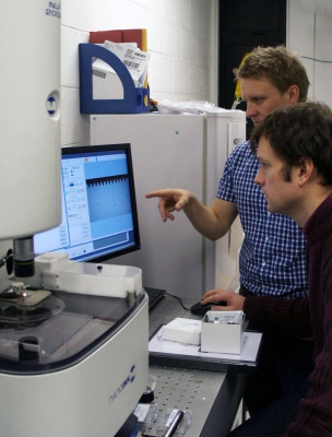
Dr. Robert Stokes (left), from NanoInk and Dr. Nicholas Laurand (right), from the Institute of Photonics at the University of Strathclyde, look at a substrate being patterned using NanoInk’s NLP 2000. The Institute of Photonics plans to use the NLP 2000 specifically for the deposition of soft materials to existing structures to generate optical effects, color conversion and for laser fabrication.

 NanoInk’s NLP 2000 System is a desktop nanofabrication system that allows researchers to rapidly design and create custom engineered and functionalized surfaces on the micro and nanoscale, using Dip Pen Nanolithography (DPN) to transfer minute amounts of materials over a large, environmentally controlled work area.

"We are excited by our initial results using the NLP 2000 in the deposition of optical materials and polymers. The patterning of soft materials using tip-based lithography builds strongly on our existing expertise and capabilities in microLED arrays. As an applications-focused research unit, we believe that many exciting research opportunities will stem from this technology," said Simon Andrews, business development manager for the Institute of Photonics. "We are also very encouraged by NanoInk’s focus on supporting application development with a view towards future commercial exploitation."

"The ability of the NLP 2000 to generate patterns of optical materials on scales wavelength or sub-wavelength dimensions is clearly aligned with the strategy and capability of the Institute of Photonics," said Robert Marchmont, general manager of Europe, the Middle East and Africa, NanoInk. "With three of NanoInk’s DPN systems installed in close proximity, and the strong collaboration between Professors Martin Dawson, Peter Skabara and Duncan Graham, the University of Strathclyde has developed into a key center of excellence for DPN in optical nanoscience."

NanoInk Inc. is an emerging growth technology company specializing in nanometer-scale manufacturing and applications development for the life sciences, engineering, pharmaceutical, and education industries. NanoInk’s NanoFabrication Systems Division brings sophisticated nanofabrication to the laboratory desktop in an easy to use and affordable setting. More information is available at www.nanoink.net/divisions.html#NanoFabrication.

The Institute of Photonics is a commercially oriented research unit, part of the University of Strathclyde. The Institute’s key objective is to bridge the gap between academic research and industrial applications and development in the area of photonics. More information is available at www.photonics.ac.uk.

Follow Small Times on Twitter.com by clicking www.twitter.com/smalltimes. Or join our Facebook group

January 19, 2011 — United Microelectronics Corporation (NYSE:UMC) (TWSE:2303), a semiconductor foundry, said today that it has produced customer micro electromechanical systems (MEMS) sensor products and volume production is scheduled to start this year.

This milestone comes after three years of MEMS technology development at the foundry, UMC said. Engineering samples are scheduled for the first half of 2011, with volume production to begin after that. Development of the CMOS-MEMS accelerometer has met consumer electronics application specifications (1g-16g) and achieved readiness for volume production.

Copyright 2011 Normans Media Limited All Rights Reserved

Follow Small Times on Twitter.com by clicking www.twitter.com/smalltimes. Or join our Facebook group

January 17, 2011 – EON: Enhanced Online News – BUSINESSWIRE — OMRON Corporation (TOKYO:6645)(ADR:OMRNY) will release the D6F-70, a 70L/min MEMS flow sensor optimized for measuring the gas flow rate of fuel cell systems. Omron also plans to release in FY2011 a similar MEMS flow sensor capable of measuring up to 200L/min.

These products will greatly enhance Omron’s MEMS flow sensor lineup.

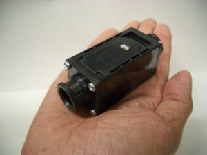
Click to EnlargeThe D6F-70 MEMS Flow Sensor is capable of measuring up to 70L/min- an improvement of 20L/min from the current model- all with a very high level of accuracy thanks to Omron’s MEMS technology.
The detrimental effect of pump vibration has been reduced by 90% compared to existing models allowing a higher level of flow sensing accuracy. The D6F-70 70L/min flow sensor is almost the same size (84.6 × 32 × 30mm) as existing 50L/min sensors. This was made possible with a unique new flow structure.

OMRON added sensors with P14-type quick connectors to the series. It is the standard connector type for fuel cell systems in Japan and significantly reduces the time required for pipe connection work.

OMRON expects 200,000 units to be used in fuel cell systems in FY2013.

Such sensors are needed to control the 70L/min flow rate of air as it reacts with hydrogen in home-use fuel cell systems. With this new addition to the lineup, Omron can now provide flow sensors suitable for use in all home-use fuel cell systems. The new sensor is also available with a standard P14-type quick connector that enables easier connection to fuel cell systems.

Higher flow rate types are increasingly necessary for industrial-use high power generation fuel cells. Omron’s 200L/min type flow sensor scheduled for release in FY2011 will be able to meet the requirements of almost any type of fuel cell system. They will also enable wider usage in medical equipment applications, and are expected to open the door to a range of other new applications.

Fuel cells and other such environmentally friendly products are increasingly moving into the mainstream, and it is predicted that their use will become widespread globally in the near future. Our flow sensors improve the operational efficiency of fuel cells making them an even more attractive option for a wide range of applications.

Specifications:
Model number D6F-70AB71 
Flow range 0 to 70 L/min 
Medium Air 
Power supply DC10.4 to 26.4V 
Output DC1.0 to 5.0V 
Size 84.6 × 32 × 30mm
Accuracy ±3%F.S. at 25C. 
Operating temperature -10 to +60C. 
Operating humidity 35 to 85%RH (in ice-free, condensation-free conditions)

OMRON Corporation is a global leader in the field of automation. For more information, visit OMRON’s website at http://www.omron.com/

Follow Small Times on Twitter.com by clicking www.twitter.com/smalltimes. Or join our Facebook group

January 17, 2011 – PRNewswire — The Kanzius Cancer Research Foundation (KCRF) announced that research conducted in the Kanzius/Curley Lab at The University of Texas M.D. Anderson Cancer Center has been published in the December 2010 issue of the American Association of Cancer Research’s Clinical Cancer Research journal. The manuscript ("Noninvasive Radiofrequency Field Destruction of Pancreatic Andenocarcinoma Xenografts Treated with Targeted Gold Nanoparticles" can be found under http://www.kanziuscancerresearch.org/research/published_research_manuscripts.illustrates) how Drs. Steven A. Curley and Evan S. Glazer’s studies prove that radiofrequency fields can treat pancreatic tumors, which today, kill more than 95% of diagnosed patients. Studies found that noninvasive radiofrequency (RF) fields were effective in controlling relatively large malignant pancreatic tumors. Additionally, this process took place without any injury to surrounding tissue or changes in non-human subject behavior.

Click to EnlargeThe manuscript describes the process as non-human subjects are exposed to 10 minutes of nonionizing radiofrequency (RF) radiation followed by 36 hours of treatment using targeted gold nanoparticles (AuNP). This revolutionary design shows that the Kanzius RF machine alongside these particular nanoparticles create an effective formula for controlling pancreatic cancer cells. Also read: Gold nanoparticles could ‘cook’ cancer cells

"John Kanzius, who created the RF device, once envisioned a cancer treatment that would be both effective and have zero side effects," remarked Curley, Chief of Gastrointestinal Tumor Surgery and Program Director of Multidisciplinary Gastrointestinal Cancer Care at The University of Texas M. D. Anderson Cancer Center. "These experiments demonstrate that the Kanzius RF device controls pancreatic cancer cells without any damage to nearby cells, or normal tissues and organs. We still have a lot of work to do but this is an important proof of principle."

"These recent findings bring us one step closer to producing an effective, noninvasive cancer treatment that doesn’t have the side effects associated with current treatments like chemotherapy and radiation," said Mark Neidig, Executive Director of KCRF. Also read: Nano-particles can lessen cancer drug side effects: Animal tests confirm

The Kanzius Cancer Research Foundation is a 501(c)(3) non-profit organization with a mission to create national and global awareness of the potentials of the Kanzius Noninvasive Radiowave Cancer Treatment, and to help accelerate the speed at which this research progresses to human trials. For more information about the Kanzius research, visit www.Kanzius.org.

Follow Small Times on Twitter.com by clicking www.twitter.com/smalltimes. Or join our Facebook group

January 17, 2011 — Camera Particle Tracking (CPT) technology  is a technique developed at Glasgow University to enhance quantitative measurement capability in research involving optical trapping.

Optical trapping is a difficult and multi-faceted technique, involving lasers, microscopes, imaging systems, specialist software and complex opto-mechanical design. It can take one to two years for a post-doc student to DIY build and calibrate a laser tweezer before they can begin meaningful experiments. Elliot Scientific turnkey optical trapping systems work "straight out the box," allowing research to begin from day one.

Laser tweezers have become an invaluable tool for measuring and exerting forces in the microscopic world. The picoNewton forces that light can exert on minuscule particles have empowered scientists, particularly those in biomedicine, enabling them to perform important studies on single molecules, cells and colloids without inflicting damage.

Current systems can only measure the force exerted on one particle, but the CPT technology will enable the collection of data from multiple particles at a higher rate. This will allow for:

  • Convenient trap calibration by thermal analysis
  • Improved trap stiffness measurements
  • Multiple particle tracking within microfluidic channels
  • Orbital angular momentum measurements
  • Viscosity measurements at several points simultaneously.

In December 2010, following selection by the University of Glasgow, Elliot Scientific was the first company to benefit from the University’s Easy Access IP initiative, a scheme designed to freely transfer some of the University’s technical, scientific and medical intellectual property to research and industry for the benefit of all.

Elliot Scientific will demonstrate their first system incorporating CPT technology at the American Biophysical Society Annual Meeting, Baltimore, in March 2011.

Elliot Scientific is a major supplier of opto-mechanic, laser, cryogenic, magnetic, telecom and datacom components and systems to the scientific, research and industrial communities. Learn more at www.elliotscientific.com

Follow Small Times on Twitter.com by clicking www.twitter.com/smalltimes. Or join our Facebook group