Tag Archives: Small Times Magazine

January 17, 2011 — Camera Particle Tracking (CPT) technology  is a technique developed at Glasgow University to enhance quantitative measurement capability in research involving optical trapping.

Optical trapping is a difficult and multi-faceted technique, involving lasers, microscopes, imaging systems, specialist software and complex opto-mechanical design. It can take one to two years for a post-doc student to DIY build and calibrate a laser tweezer before they can begin meaningful experiments. Elliot Scientific turnkey optical trapping systems work "straight out the box," allowing research to begin from day one.

Laser tweezers have become an invaluable tool for measuring and exerting forces in the microscopic world. The picoNewton forces that light can exert on minuscule particles have empowered scientists, particularly those in biomedicine, enabling them to perform important studies on single molecules, cells and colloids without inflicting damage.

Current systems can only measure the force exerted on one particle, but the CPT technology will enable the collection of data from multiple particles at a higher rate. This will allow for:

  • Convenient trap calibration by thermal analysis
  • Improved trap stiffness measurements
  • Multiple particle tracking within microfluidic channels
  • Orbital angular momentum measurements
  • Viscosity measurements at several points simultaneously.

In December 2010, following selection by the University of Glasgow, Elliot Scientific was the first company to benefit from the University’s Easy Access IP initiative, a scheme designed to freely transfer some of the University’s technical, scientific and medical intellectual property to research and industry for the benefit of all.

Elliot Scientific will demonstrate their first system incorporating CPT technology at the American Biophysical Society Annual Meeting, Baltimore, in March 2011.

Elliot Scientific is a major supplier of opto-mechanic, laser, cryogenic, magnetic, telecom and datacom components and systems to the scientific, research and industrial communities. Learn more at www.elliotscientific.com

Follow Small Times on Twitter.com by clicking www.twitter.com/smalltimes. Or join our Facebook group

January 14, 2011 — Electron microscopes are among the most widely used scientific and medical tools for studying and understanding a wide range of materials, from biological tissue to miniature magnetic devices, at tiny levels of detail. Now, researchers at the National Institute of Standards and Technology (NIST) have found a novel and potentially widely applicable method to expand the capabilities of conventional transmission electron microscopes (TEMs). Passing electrons through a nanometer-scale grating, the scientists imparted the resulting electron waves with so much orbital momentum that they maintained a corkscrew shape in free space. 

Click to Enlarge
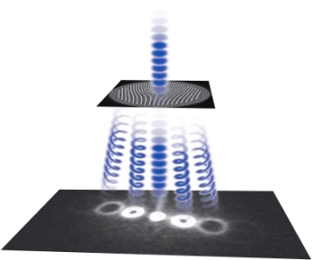
Figure. NIST researchers twisted the flat electron wavefronts into a fan of helices using a very thin film with a 5-micron-diameter pattern of nanoscale slits, which combines the wavefronts to create spiral forms similar to a pasta maker extruding rotini. This method produces several electron beams fanning out in different directions, with each beam made of electrons that orbit around the direction of the beam. Source: B. McMorran/NIST

 
The development opens the possibility of adapting transmission electron microscopy, which can see tinier details than optical microscopy and can study a wider range of materials than scanning probe microscopy, for quick and inexpensive imaging of a larger set of magnetic and biological materials with atomic-scale resolution.

"The spiral shape and angular momentum of these electrons will let us look at a greater variety of materials in ways that were previously inaccessible to TEM users," said Ben McMorran, one of the authors of the research paper. "Outfitting a TEM with a nanograting like we used in our experiment could be a low-cost way to dramatically expand the microscope’s capabilities."

Although NIST researchers were not the first to manipulate a beam of electrons in this way, their device was much smaller, separated the fanned out beams 10 times more widely than previous experiments, and spun up the electrons with 100 times the orbital momentum. This increase in orbital momentum enabled them to determine that the electron corkscrew, while remarkably stable, gradually spreads out over time. The group’s work is reported in the January 14, 2011 issue of the journal Science (*B. McMorran, A. Agrawal, I. Anderson, A. Herzing, H. Lezec, J. McClelland, and J. Unguris. Electron Vortex Beams with High Quanta of Orbital Angular Momentum. Science) Read the abstract at http://www.sciencemag.org/content/331/6014/192.abstract?sid=902b04d6-7f65-4035-821d-1bcf07986f24

Electrons in electron beams behave like rippling waves that move through space like a wave of light, McMorran said. Unlike wavefronts of light, which are hundreds of nanometers apart (a distance called the wavelength), the wavelengths of electrons are measured in picometers (trillionths of a meter), which make them excellent for imaging tiny objects such as atoms because of their comparable dimensions. In an ordinary electron beam, the electron wavefronts are relatively flat and uniform.

To spin up the electrons and give them orbital momentum, the NIST researchers twisted the flat electron wavefronts into a fan of helices using a very thin film with a 5-micron-diameter pattern of nanoscale slits. The pattern affects the shape of the electron wavefronts passing through it, amplifying some of the wave peaks and eliminating some of the wave valleys, to create a spiral form similar to a pasta maker extruding rotini. This method produces several electron beams fanning out in different directions, with each beam made of electrons that orbit around the direction of the beam.

The researchers knew they were successful because when they detected the electrons – which were recorded as millions of individual particles building up an image – they had formed donut-like or spiral patterns, indicating a helical shape.

Transmission electron microscopy creates images by shooting trillions of electrons through an object and measuring their absorption, deflection and energy loss. TEMs equipped with corkscrew electron beams could also monitor how the particles exert torque on a material and how a material affects the spiral shape of transmitted electrons, helping scientists build a more complete picture of the material’s structure.

For example, these special electron beams have the potential to help obtain more information from magnetic materials.

"Magnetism, at its most fundamental, results from charges spinning and orbiting," McMorran said. "So an electron beam that itself carries angular momentum makes a good tool for probing magnetic materials."

A beam of corkscrew-shaped electrons, when interacting with a specimen, can exert torque on the material, by exchanging angular momentum with its atoms.  In this way, the corkscrew electrons could obtain more information in the process than beams with ordinary electrons, which do not carry this orbital angular momentum.

This technique could also help improve TEM images of transparent objects like biological specimens. Biological material can be difficult to image in ordinary TEMs because electrons pass through it without deflecting. But by using corkscrew electron beams, researchers hope to provide high-contrast, high-resolution images of biological samples by looking at how the spiral wavefronts get distorted as they pass through such transparent objects.

While these imaging applications have not yet been demonstrated, producing corkscrew electrons with nanogratings in a TEM provides a significant step toward expanding the capabilities of existing microscopes.

Follow Small Times on Twitter.com by clicking www.twitter.com/smalltimes. Or join our Facebook group

January 14, 2011 — A simple technique to make a common virus-killing material significantly more effective is a breakthrough from the Rice University labs of Andrew Barron and Qilin Li. Silicone grease, silica, or silicic acid can treat titanium dioxide nanoparticles for increased virus-killing efficiency.

Rather than trying to turn the process into profit, the researchers have put it into the public domain. They hope wide adoption will save time, money and perhaps even lives. The Rice professors and their team reported in Environmental Science and Technology, an American Chemical Society journal, that adding silicone to titanium dioxide, a common disinfectant, dramatically increases its ability to degrade aerosol- and water-borne viruses. Read the abstract at http://pubs.acs.org/doi/abs/10.1021/es102749e

Click to Enlarge
From left, Professor Qilin Li, graduate student Michael Liga, alumna Huma Jafry and Professor Andrew Barron have published a paper outlining their method to dramatically improve the effectiveness of a common disinfectant.

"We’re taking a nanoparticle that everyone’s been using for years and, with a very simple treatment, we’ve improved its performance by more than three times without any real cost," said Barron, Rice’s Charles W. Duncan Jr.-Welch Professor of Chemistry and a professor of materials science. Barron described himself as a "serial entrepreneur," but saw the discovery’s potential benefits to society as being far more important than any thoughts of commercialization.

Barron said titanium dioxide is used to kill viruses and bacteria and to decompose organics via photocatalysis (exposure to light, usually ultraviolet). The naturally occurring material is also used as a pigment in paints, in sunscreen and even as food coloring.

"If you’re using titanium dioxide, just take it, treat it for a few minutes with silicone grease or silica or silicic acid, and you will increase its efficiency as a catalyst," he said.

Barron’s lab uses "a pinch" of silicon dioxide to treat a commercial form of titanium dioxide called P25. "Basically, we’re taking white paint pigment and functionalizing it with sand," he said.

Disinfecting a volume of water that once took an hour would now take minutes because of the material’s enhanced catalytic punch, Barron said. "We chose the Yangtze River as our baseline for testing, because it’s considered the most polluted river in the world, with the highest viral content," he said. "Even at that level of viral contamination, we’re getting complete destruction of the viruses in water that matches the level of pollution in the Yangtze."

Using a smaller amount of treated P25 takes longer but works just as well, he said. "Either way, it’s green and it’s cheap."

The team started modifying titanium dioxide two years ago. Li, an assistant professor in civil and environmental engineering whose specialties include water and wastewater treatment, approached Barron to help search for new photocatalytic nanomaterials to disinfect drinking water.

The revelation came when students in Barron’s lab heated titanium dioxide, but it wasn’t quite the classic "aha!" moment. Graduate student and co-author Michael Liga saw the data showing greatly enhanced performance and asked fellow graduate student Huma Jafry what she had done. Jafry, the paper’s first author, said, "I didn’t do anything." When Barron questioned Jafry, who has since earned her doctorate, he discovered she used silicone grease to seal the vessel of P25 before heating it. Subsequent testing with nonsilicone grease revealed no change in P25’s properties, whether the sample was heated or not. Remarkably, Barron said, further work with varying combinations of titanium dioxide and silicone dioxide found the balance between the two at the time of the discovery was nearly spot-on for maximum impact.

Barron said binding just the right amount of silica to P25 creates an effect at the molecular level called band bending. "Because the silicone-oxygen bond is very strong, you can think of it as a dielectric," he said. "If you put a dielectric next to a semiconductor, you bend the conduction and valence bands. And therefore, you shift the absorption of the ultraviolet (used to activate the catalyst)."

Bending the bands creates a path for electrons freed by the UV to go forth and react with water to create hydroxyl radicals, an oxidant responsible for contaminant degradation and the most significant reactive agent created by titanium dioxide. "If your conduction band bends to the degree that electrons find it easier to pop out and do something else, your process becomes more efficient," Barron said.

Li saw great potential for enhanced P25. In developed countries, photo reactors designed to take advantage of the new material in centralized treatment plants could more efficiently kill bacteria and inactivate viruses in water supplies while minimizing the formation of harmful disinfection byproducts, she said.

But the greatest impact may be in developing nations where water is typically disinfected through the SODIS method, in which water is exposed to sunlight for its heat and ultraviolet radiation.

"In places where they don’t have treatment plants or even electricity, the SODIS method is great, but it takes a very long time to make water safe to drink," Li said. "Our goal is to incorporate this photocatalyst so that instead of taking six hours, it only takes 15 minutes."

"Here’s a way of taking what is already a very good environmental catalyst and making it better," Barron said. "It works consistently, and we’ve done batch after batch after batch of it now. The methodology in the paper is the one we routinely use. As soon as we buy P25, we treat it."

The Robert A. Welch Foundation, the U.S. Navy and the National Science Foundation Center for Biological and Environmental Nanotechnology supported the research.

Follow Small Times on Twitter.com by clicking www.twitter.com/smalltimes. Or join our Facebook group

January 13, 2011 – BUSINESS WIRE — Tegal Corporation (NASDAQ:TGAL), specialized equipment maker for the fabrication of advanced MEMS, power ICs and optoelectronic devices, received an order from the Fraunhofer Institute for Microelectronic Circuits and Systems in Duisburg, Germany for a Tegal 200 SE DRIE system equipped with the new Tegal ProNova2 reactor.

The Tegal 200 SE DRIE system will be shipped and installed at the customer’s site in early CY2011, and will support Fraunhofer IMS’ mission to develop and produce microelectronic system solutions by combining mixed-signal ICs and integrated microsystems (MEMS) devices built using a state-of-the-art equipment set and "more than Moore" thinking.

The Tegal 200 SE silicon DRIE system order from this first-time Tegal DRIE customer is the result of a thorough competitive evaluation Fraunhofer IMS performed on a broad range of silicon DRIE tools and tool suppliers.

"The capabilities of the Tegal 200 SE are convincing for us due to the Tegal system’s demonstrated high deep silicon etch performance and high process flexibility, including oxide and isotropic silicon etch. We believe that this equipment excellently meets our needs for advanced MEMS development," said Dr. Andreas Goehlich from the Fraunhofer IMS.

"Fraunhofer IMS is well-known for technological leadership in integrated microsystems, and we are very pleased to have received this important silicon DRIE tool order," said Jim Apffel, DRIE product manager at Tegal Corporation, adding that the ProNova2 DRIE process module an advanced silicon DRIE process module for 200mm applications and the Tegal 200 SE is the best-adapted DRIE solution for 3D-IC and MEMS volume manufacturing.

The Tegal 200 SE is designed to achieve high throughput with low cost of ownership in production applications, thanks to the combination of extended time between cleaning, minimal wafer edge exclusion, high silicon etch rates, excellent process stability and highly uniform etching.

The Tegal ProNova2 reactor is targeted for fast-growing 200mm MEMS and 3D IC applications. It was built to out-perform comparative tools’ etch rates and increase DRIE productivity and yields. In addition to sustained high etch rates, the new ProNova2 reactor offers a three-fold improvement in ion uniformity over standard ICP sources. For some applications, the higher ion uniformity enables a more than 40% improvement in etch selectivity.

Fraunhofer IMS in Duisburg covers the broad spectrum of industrial and automotive microelectronics. In addition, new solutions in the sector of Health & Senior Care are being tested and developed further in the Fraunhofer-inHaus-Center. As a member of the Fraunhofer Gesellschaft, Fraunhofer IMS carries out research, development and pilot fabrication of microelectronic solutions for industrial and public clients.

Tegal is an innovator of specialized production solutions for the fabrication of advanced MEMS, power ICs and optoelectronic devices. Tegal silicon DRIE tools are used in numerous research and development laboratories throughout the world, engaging in both commercial and academic research programs, and are also found in MEMS foundries and other dedicated commercial High Volume Manufacturing lines worldwide. Learn more at www.tegal.com.

Follow Small Times on Twitter.com by clicking www.twitter.com/smalltimes. Or join our Facebook group
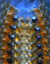
January 13, 2011 — The black teeth of an Eastern beaded chiton, a sea mollusk, are used for scraping algae from rocks. They are capped with one of the hardest biominerals known, a nanocomposite of magnetite and chitin-based fibers.

Click to EnlargeTeeth and bone are important and complex structures in humans and other animals, but little is actually known about their chemical structure at the atomic scale. What exactly gives them their renowned toughness, hardness and strength? How do organisms control the synthesis of these advanced functional composites?

The interface between the organic and inorganic materials plays a large role in controlling properties and structure, said Derk Joester, senior author of the paper. How do organisms make and control these materials? We need to understand this architecture on the nanoscale level to design new materials intelligently. Otherwise we really have no idea what is going on.

Joester is the Morris E. Fine Junior Professor in Materials and Manufacturing at the McCormick School of Engineering and Applied Science. Lyle Gordon, a doctoral student in Joester’s lab, is the other author of the paper.

Using a highly sophisticated atomic-scale imaging tool on the sea creature’s tooth, the Northwestern University researchers have peeled away some of the mystery of organic/inorganic interfaces that are at the heart of tooth and bone structure. They are the first to produce a three-dimensional map of the location and identity of millions of individual atoms in the complex hybrid material that allows the animal to literally chew rock.

Joester and Gordon imaged teeth of the chiton, a tiny marine mollusk, because much is known about the biomineralization process. The chiton lives in the sea and feeds on algae found on rocks. It continually makes new rows of teeth — one a day — to replace mature but worn teeth; in conveyor-belt fashion, the older teeth move down the creature’s tongue-like radula toward the mouth where it feeds.

Chiton teeth resemble human teeth in that they have a hard and tough outer layer — equivalent to our enamel — and a softer core. Instead of enamel, the rock-chewing chitons use magnetite, a very hard iron oxide, which gives their teeth a black luster.

Demonstrating that atom-probe tomography (APT) can be used to interrogate such materials opens up the possibility of tracking fluoride in teeth and cancer and osteoporosis drugs in bone (at previously inaccessible length scales). The detailed knowledge of organic/inorganic interfaces also will help scientists rationally design useful new materials — flexible electronics, polymers and nanocomposite materials, such as organic photovoltaics — that combine the best properties of organic and inorganic materials.

The researchers set out to find the organic fibers they knew to be an important part of the tooth’s structure, buried in the tough outer layer of the tooth, made of magnetite. Their quantitative mapping of the tooth shows that the carbon-based fibers, each 5 to 10 nanometers in diameter, also contained either sodium or magnesium ions. Joester and Gordon are the first to have direct proof of the location, dimension and chemical composition of organic fibers inside the mineral.

They were surprised by the chemical heterogeneity of the fibers, which hints at how organisms modulate chemistry at the nanoscale. Joester and Gordon are anxious to learn more about how the organic fibers interface with the inorganic minerals, which is key to understanding hybrid materials.

The tooth’s toughness comes from this mix of organic and inorganic materials and the interfaces between them, Joester said. While this is, in principle, well known, we may have overlooked how subtle changes in the chemical makeup of nanoscale interfaces may play a role in, for instance, bone formation or the diffusion of fluoride into tooth enamel. In this regard, atom-probe tomography has the potential to revolutionize current understanding.

Atom-probe tomography produces an atom-by-atom, 3D reconstruction of a sample with sub-nanometer resolution. But many in the field didn’t think APT would work to analyze a material made up of organic and inorganic parts. Northwestern’s David Seidman, a leader in the field, uses APT to study metals. The school also has two of the few APT instruments in the US. Seidman, Walter P. Murphy Professor of Materials Science and Engineering, encouraged Joester to take the risk and use APT to study biological architectures. The scientists also were able to exchange ideas with the engineers developing 3D atom-probe instruments at CAMECA, a scientific instrumentation company in nearby Madison, WI.

The researchers extracted micron-sized samples from the leading edge of the chiton tooth. Using a focused ion beam (FIB) tool at the Northwestern University Atomic and Nanoscale Characterization Experimental Center core facility, these samples were fashioned into very sharp tips (<20nm across). The process is reminiscent of sharpening a pencil, with a supercharged stream of gallium ions.

The APT technique applies an extremely high electric field to the sample; atoms on the surface ionize, fly off, and hit an imaging detector. The atoms are stripped off atom-by-atom and layer-by-layer. Computer methods then are used to calculate the original location of the atoms, producing a 3D map or tomogram of millions of atoms within the sample.

The results are published today by the journal Nature. The title of the paper is Nanoscale chemical tomography of buried organicinorganic interfaces in the chiton tooth. Read the abstract here

Joester and Gordon now are studying the tooth enamel of a vertebrate and plan to apply APT to bone, which is also made of organic and inorganic parts, to learn more about its nanoscale structure.

The National Science Foundation and the Canadian National Sciences and Engineering Research Council supported the research.

Courtesy of Megan Fellman, Northwestern University. Copyright 2011 States News Service

Follow Small Times on Twitter.com by clicking www.twitter.com/smalltimes. Or join our Facebook group

January 13, 2011 — Yole Développement released details of its upcoming report, MEMS Manufacturing & Packaging. This report analyzes the main MEMS manufacturing evolution. MEMS drivers include size, cost, and performance, though in different ways than ICs. New MEMS manufacturing and packaging technologies and specific materials are necessary.

"With this report, our aim is to provide understanding of current challenges of MEMS manufacturing, packaging & materials. For each MEMS manufacturing step, bottlenecks and challenges are highlighted," explained Dr Eric Mounier, project manager at Yole Développement. Yole Développement’s approach is to analyze the MEMS industry evolution, per MEMS devices (inertial MEMS, magnetometers, pressure sensors, etc). Technical & market data covers the period 2000-2020. This study includes cost analysis, technical trends, impact on MEMS equipment & materials, manufacturing tools (DRIE, sacrificial release, etc), and engineered wafers & materials.

Click to Enlarge
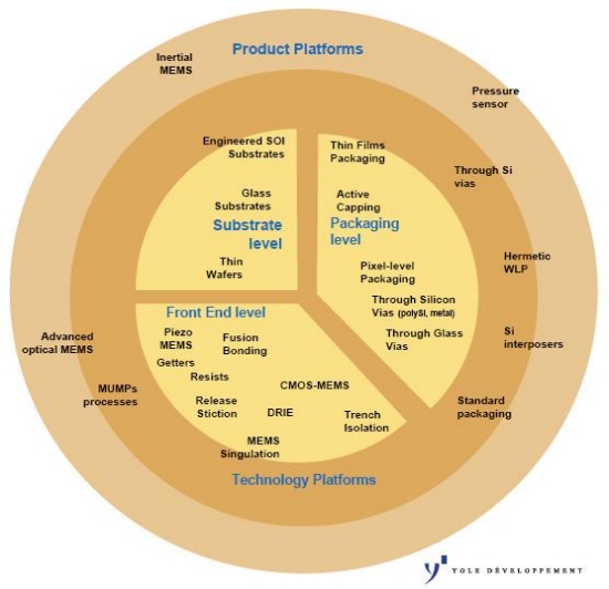
Figure. Example of different MEMS manufacturing & packaging trends analyzed in the report “MEMS Manufacturing & Packaging” Source: Yole.

Although MEMS technologies have not been driven by the same size demands as ICs, MEMS manufacturing is not just standing still. The fast growing MEMS markets, now led by consumer applications, are:

  • Size-drive: for demanding consumer applications like smart phones and laptops
  • Performance-driven: for high-end applications like aerospace
  • Cost-driven: for high-volume applications like cell phones, automotive and game consoles

New MEMS manufacturing and packaging technologies and specific materials are necessary for solving these issues. Yole Développement’s report highlights the future challenges for MEMS production and packaging. From bulk micromachining to surface micromachining and then to SOI, MEMS technology has been following a well-defined evolutionary technical roadmap with 3D integration being the next possible step. The report includes manufacturing trends for the different MEMS devices in terms of processes, new packaging approaches, 3D integration, CMOS MEMS integration, new materials such as structured wafers, and more.

MEMS processes are analyzed at:

  • The substrate level: engineered SOI, glass, thin wafers
  • Front End level: piezo materials, getters, bonding, resists, CMOS MEMS, release stiction, DRIE, singulation, lithography, etching, sacrificial release, CAD tools
  • The packaging level: thin film packaging, active capping, pixel-level packaging, through glass vias, through Si vias
  • Technology platforms: TSV, hermetic WLP, interposer, standard packaging, MUMPS process, testing

This report analyzes the current major MEMS manufacturing trends and presents some clues for understanding the next evolution in terms of die size, cost, packaging. Among other MEMS technologies to watch for the future, Yole identified:

  • At the substrate level: SOI, glass, thin wafers;
  • At MEMS die level: getters, fusion bonding, release stiction, singulation, CMOS MEMS, DRIE, trench isolation;
  • At the packaging level: TGV, TSV, pixel-level packaging, thin film capping, active capping.

For all the analyzed MEMS technologies, wafer forecasts 2009-2015 by type of step (DRIE, wafer bonding, sacrificial etch, through Si vias, thin films packaging, CMOS MEMS, thin wafers) are estimated.

Companies cited in the MEMS report:
36Deg,  Accretech, AD, Aichi Steel, Air Products, AKM, Akustica, ALSI, Amkor, AML, APM, ASE, ASML, AST, Avago, Aviza, Ayumi, Bal-Tec, Baolab, Berliner Glass, BOC Edwards, Bosch, Brewer, Coventor, Dalsa, Dicon, Discera, Disco, Elpida, Entrepix, ePack, Epcos, EVG, FhG ISiT, FLIR, FocusTest, Freescale, FSI, Hamamatsu, Hitachi Metals, HP, IBM, IDEX, Idonus, Ikonics, IMT, Infineon, Invensense, Ixmotion, JDSU, Kionix, Knowles, LAM Research, Lemoptix, Leti, Lumedyne, Memscap, Memscore, Memsic, Memsstar, Memstech, MEMTronics, Micralyne, Micro Devices Laboratory, Microstaq, Mitsubishi Electric, Nanoplas, NEC Schott, NeoPhotonics, NovioMEMS, Okmetic, Omron, Panasonic Factory Solutions, Penta Technology, piezoVolume, Plan Optik, Polight, Primaxx, QinetiQ, QMT, RFMD, SAES, Samsung, Sandia National Labs, Santec, Semitool, Sensonor, Shell, Silex, Silicon Clocks, SiTime, Solidus Technologies, SPEA, Sporian Microsystems, STM, STPS, SUSS MicroTec, Tango, Tecnisco, Tegal, TEL, TI, TMT, TopCon, Toshiba, Tousimis, Tronics’, TSMC, Ulcoat, Ulis, UltraTechSteppers, Ulvac, Umicore, Veratag, Visera, Vi Technology, VTI, Xactix, XFAB, Xintec.

DRIE and wafer bonders are the technologies subject to major evolution. "Both technologies are increasingly used for 3D TSV in the mainstream semiconductor business. Wafer bonding is the direct competitor to the CMOS MEMS approach," says Dr Eric Mounier. For example, microbolometer players are more and more considering a wafer bonding approach to stack the MEMS to the ROIC wafer.

CMOS MEMS is likely to be restricted to very specific applications where MEMS arrays will need very close electronic processing. For all other cases, it will depend on MEMS product cycle time, flexibility, cost, integration, market demand and power consumption.

In 2011, simplification of manufacturing remains an objective: Yole Développement’s MEMS law of "One product, one process, one package" still rules. Will it still rule in 2020? The current work on technology and product platforms aims to overcome Yole Développement’s MEMS law. But this approach will be custom-made standard processes. By 2020, it is likely that MEMS fabs will have developed internal standard process blocks, but with fab-specific standard tools. The technology/product platforms currently proposed by some MEMS foundries are an interesting approach. Technology platforms can be used to create their own product platform.
 
Dr. Eric Mounier has a PhD in microelectronics from the INPG in Grenoble and is in charge of market analysis for MEMS, equipment & material. The report, "MEMS Manufacturing & Packaging," will be available in February 2011. Yole Développement is a group of companies providing market research, technology analysis, strategy consulting, media and finance services. More information is available at www.yole.fr

Follow Small Times on Twitter.com by clicking www.twitter.com/smalltimes. Or join our Facebook group
January 12, 2011 — Researchers at MIT and Brigham and Women’s Hospital have shown that they can deliver the cancer drug cisplatin much more effectively and safely in a form that has been encapsulated in a nanoparticle, targeted to prostate tumor cells and activated once it reaches its target.

Using the new particles, the researchers were able to successfully shrink tumors in mice, using only one-third the amount of conventional cisplatin needed to achieve the same effect. That could help reduce cisplatin’s potentially severe side effects, which include kidney damage and nerve damage.

In 2008, the researchers showed that the nanoparticles worked in cancer cells grown in a lab dish. Now that the particles have shown promise in animals, the team hopes to move on to human tests.

Click to Enlarge"At each stage, it’s possible there will be new roadblocks that will come up," noted Stephen Lippard, the Arthur Amos Noyes Professor of Chemistry and a senior author of the paper, which appears in the Proceedings of the National Academy of Sciences the week of Jan. 10. Additional animal testing is needed before the cisplatin-carrying particles can go into human clinical trials, says Farokhzad. "At the end of the day, if the development results are all promising, then we would hope to put something like this in humans within the next three years," he says.

Click to EnlargeOmid Farokhzad, associate professor at Harvard Medical School and director of the Laboratory of Nanomedicine and Biomaterials at Brigham and Women’s Hospital, is also a senior author of the paper. Shanta Dhar, a postdoctoral associate in Lippard’s lab, and Nagesh Kolishetti, a postdoctoral associate in Farokhzad’s lab, are co-lead authors.

Cisplatin, which doctors began using to treat cancer in the late 1970s, destroys cancer cells by cross-linking their DNA, which ultimately triggers cell death. Despite its adverse side effects, which also include nerve damage and nausea, about half of all cancer patients receiving chemotherapy are taking platinum drugs. Read about other MIT research on cisplatin.

Conventional cisplatin has a relatively short lifetime in the bloodstream. Only about 1% of the dose given to a patient ever reaches the tumor cells’ DNA, and about half of it is excreted within an hour of treatment.

To prolong the time in circulation, the researchers decided to encase a derivative of cisplatin in a hydrophobic nanoparticle. First, they modified the drug, which is normally hydrophilic, with two hexanoic acid units. That enabled them to encapsulate the resulting prodrug — a form that is inactive until it enters a target cell — in a nanoparticle. To help the nanoparticles reach their target, the researchers also coated them with molecules that bind to PSMA (prostate specific membrane antigen), a protein found on most prostate cancer cells.

Using this approach, much more of the drug reaches the tumor. The researchers found that the nanoparticles circulated in the bloodstream for about 24 hours, at least 5 times longer than un-encapsulated cisplatin. They also found that it did not accumulate as much in the kidneys as conventional cisplatin.

After showing the nanoparticles’ improved durability in the blood, the researchers tested their effectiveness by treating mice implanted with human prostate tumors. They found that the nanoparticles reduced tumor size as much as conventional cisplatin over 30 days, but with only 30% of the dose.

This type of nanoparticle design could be easily adapted to carry other types of drugs, or even more than one drug at a time, as the researchers reported in a PNAS paper last October. It could also be designed to target tumors other than prostate cancer, as long as those tumors have known receptors that could be targeted. One example is the Her-2 receptor abundant in some types of breast cancer, says Lippard. Read about breast cancer research involving MEMS.

The particles tested in this paper are based on the same design as particles developed by Farokhzad and MIT Institute Professor Robert Langer that deliver the cancer drug docetaxel. A Phase I clinical trial to assess those particles began last week, run by BIND Biosciences.

Source: "Targeted delivery of cisplatin prodrug for safer and more effective prostate cancer therapy in vivo," by Shanta Dhar, Nagesh Kolishetti, Stephen J. Lippard, and Omid C. Farokhzad. Proceedings of the National Academy of Sciences, 10, January 2011.

Funding: National Cancer Institute, National Institute of Biomedical Imaging and Bioengineering Grant, Koch-Prostate Cancer Foundation Award in Nanotherapeutics.

Courtesy of Anne Trafton, MIT News Office, www.mit.edu

Follow Small Times on Twitter.com by clicking www.twitter.com/smalltimes. Or join our Facebook group

January 12, 2011 – GLOBE NEWSWIRE — Northrop Grumman Corporation (NYSE:NOC) announced that its Scalable Space Inertial Reference Unit (Scalable SIRU) has been selected as the inertial reference unit of choice for Boeing Space and Intelligence Systems satellite platforms.

Under the terms of a strategic agreement between Boeing and Northrop Grumman, the Scalable SIRU will be included as part of the baseline design for Boeing satellites over the next two years.

"Northrop Grumman’s Scalable SIRU provides outstanding performance that plays an important role in mission success and features the space-proven reliability needed for the wide variety of Boeing missions," said Susan Sloan, vice president of space systems for Northrop Grumman’s Navigation Systems Division.

The Scalable SIRU is a high-precision, long-life attitude control solutions supporting commercial, government and civil space missions. Northrop Grumman’s Scalable SIRU and its predecessor, the space inertial reference unit (SIRU), supply critical rotation rate data for use in satellites and space vehicles for stabilization, pointing and attitude control.

Northrop Grumman’s Scalable SIRU was recently launched aboard the Boeing-built SkyTerra 1 next-generation mobile communications satellite and is performing as part of the satellite’s attitude control system.

At the heart of the Scalable SIRU is Northrop Grumman’s patented hemispherical resonator gyro (HRG) technology, which has operated in space without a mission failure for over 16 million hours since the product first entered service in February, 1996. Installed in Northrop Grumman’s space qualified inertial reference units, the HRG has been used in commercial, government and civil space missions for domestic and international customers and has been launched aboard more than 100 spacecraft. HRG missions include earth observation, communications and science applications in low earth orbit, geostationary and deep space mission profiles.

The HRG combines high performance and long life in space. It has no moving parts and its simple design, small size, low noise output and high radiation tolerance make it an ideal gyro for extended space missions.

Northrop Grumman Corporation is a global security company providing aerospace, electronics, information systems, shipbuilding and technical services to government and commercial customers worldwide. Please visit www.northropgrumman.com for more information.

Follow Small Times on Twitter.com by clicking www.twitter.com/smalltimes. Or join our Facebook group

January 12, 2011 — DiCon Fiberoptics announced that its Secure Switching Unit–an all-optical switch that allows secure fiber-optic signals to be routed as required using DiCon’s proven microelectromechanical systems (MEMS) optical switch–was a successful participant in Boeing’s first mission systems test flight of the new P-8A Poseidon aircraft. The P-8A Poseidon is a new anti-submarine, anti-surface warfare, intelligence, surveillance, and reconnaissance aircraft that the U.S. Navy plans on using to replace their existing P-3C fleet.

"We have taken our proven COTS fiber optic switch components and integrated these into the SSU in an unique way to offer Boeing a reliable way to route secure fiber optic signals in the P-8A," said Robert Schleicher, DiCon’s VP of product development. 

The Secure Switching Unit (SSU) is a complete military spec, common criteria certified, all-optical switching solution. It is a completely passive device able to route secure fiber-optic signals as an automated fiber patch panel. The SSU incorporates DiCon’s MEMS fiber-optic switches, which DiCon says are the most proven and trusted fiber-optic switches in the Telecommunications industry. Hundreds of thousands of DiCon MEMS devices have shipped since the year 2000. Their compact size, low weight, low power consumption, and ability to withstand harsh environments make them ideal for use in military applications. In addition, their frictionless design allows them to operate for billions of switch cycles.

The successful in-flight testing was completed on June 8, 2010 in the T2 aircraft, one of five test aircraft. For more information on Boeing’s P-8A Poseidon’s first in-flight test of mission systems, go to http://boeing.mediaroom.com/index.php?s=43&item=1251.

Learn more about DiCon Fiberoptics at www.diconfiberoptics.com

Also read: Fabrication and assembly of 3D MEMS devices by Daniel N. Pascual, Süss MicroTec