Author Archives: admin

DAVID W. PRICE, JAY RATHERT and DOUGLAS G. SUTHERLAND, KLA Corp., Milpitas, CA

The first three articles [1-3] in this series discussed methods that automotive semiconductor manufacturers can use to better meet the challenging quality requirements of their customers. The first paper addressed the impact of automotive IC reliability failures and the idea that combating them requires a “Zero Defect” mentality. The second paper discussed continuous improvement programs and strategies that automotive fabs implement to reduce the process defects that can become chip reliability problems. The third paper focused on the additional process control sensitivity requirements needed to capture potential latent (reliability) defects. This installment discusses excursion monitoring strategies across the entire automotive fab process so that non-conforming material can be quickly found and partitioned.

Semiconductor fabs that make automotive ICs typically offer automotive service packages (ASPs). These ASPs provide differentiated process flows – with elements such as more process control and process monitoring, or guaranteed use of golden process tools. The goal of ASPs is to help ensure that the chips produced meet the stringent reliability requirements of the automotive industry.

But even with the use of an automotive service package, excursions are inevitable, as they are with any controlled process. Recognizing this, automotive semiconductor fabs pay special attention to creating a comprehensive control plan for their critical process layers as part of their Process Failure Mode and Effects Analysis (PFMEA). The control plan details the process steps to be monitored and how they are monitored – specifying details such as the inspection sensitivity, sampling frequency and the exact process control systems to be used. A well-designed control plan will detect all excursions and keep “maverick” wafers from escaping the fab due to undersampling. Additionally, it will clearly indicate which wafers are affected by each excursion so that they can be quarantined and more fully dispositioned – thereby ensuring that non-conforming devices will not inadvertently ship.

To meet these objectives, the control plan of an automotive service package will invariably require much more extensive inspection and metrology coverage than the control plan for production of ICs for consumer products. An analysis of process control benchmarking data from fabs running both automotive and non-automotive products at the same design rule have shown that the fabs implement more defect inspection steps and more types of process control (inspection and metrology) for the automotive products. The data reveals that on average:

  • Automotive flows use approximately 1.5 to 2 times more defect inspection steps
  • Automotive flows employ more frequent sampling, both as a percentage of lots and number of wafers per lot
  • Automotive flows use additional sensitivity to capture the smaller defects that may affect reliability

The combined impact of these factors results in the typical automotive fab requiring 50% more process control capacity than their consumer product peers. A closer look reveals exactly how this capacity is deployed.

FIGURE 1 below shows an example of the number of lots between inspection points for both an automotive and a non-automotive process flow in the same fab. As a result of the increased number of inspection steps, if there is a defect excursion, it will be found much more quickly in the automotive flow. Finding the excursion sooner limits the lots at risk: a smaller and more clearly defined population of lots are exposed to the higher defect count, thereby helping serve the automotive traceability requirement. These excursion lots are then quarantined for high-sensitivity inspection of 100% of the wafers to disposition them for release, scrap, or when applicable, a downgrade to a non-automotive application.

FIGURE 1. Example demonstrating the lots at risk between inspection points for an automotive process flow (blue) and a non-automotive (baseline) process blow (pink). The automotive process flow has many more inspection points in the FEOL and therefore fewer lots at risk when a defect excursion does occur.

The additional inspection points in the automotive service package have the added benefit of simplifying the search for the root cause of the excursion by reducing the range of potential sources. Fewer potential sources helps speed effective 8D investigations4 to find and fix the problem. Counterintuitively, the increased number of inspection points also tends to reduce production cycle time due to reduced variability in the line.5

While increasing inspection capacity helps monitor and contain process excursions, there remains risk to automotive IC quality. Because each wafer may take a unique path through the multitude of processing chambers available in the fab, the sum of minor variations and marginalities across hundreds of process steps can create “maverick” wafers. These wafers can easily slip through a control plan that relies heavily on sub-sampling, allowing at-risk die into the supply chain. To address this issue, many automotive fabs are adding high-speed macro defect inspection tools to their fleet to scan more wafers per lot. This significantly improves the probability of catching maverick wafers and preventing them from entering the automotive supply chain.

Newer generation macro defect inspection tools6 can combine the sensitivity and defect capture of many older generation brightfield and darkfield wafer defect inspection tools into a single platform that can operate at nearly 150 wafers per hour, keeping cost of ownership low. In larger design rule 200mm fabs, the additional capacity often reveals multiple low-level excursions that had previously gone undetected, as shown in FIGURE 2.

FIGURE 2. The legacy sample plan of 5 wafers per lot (yellow circles) would have allowed the single maverick wafer excursion (red square) to go undetected. High capacity macro defect inspection tools can stop escapes by reducing undersampling and the associated risks.

In advanced, smaller design rule fabs, macro defect inspection tools lack the needed sensitivity to replace the traditional line monitoring and patterned wafer excursion monitoring roles occupied by broadband plasma and laser scanning wafer defect inspection tools. However, their high capacity has found an important role in augmenting the existing sample plan to find wafer-level signatures that indicate a maverick wafer.

A recent development in automotive control strategies is the use of defect inspection for die-level screening. One such technique, known as Inline Defect Part Average Testing (I-PAT™), uses outlier detection techniques to further enhance the fab’s ability to recognize die that may pass electrical test but become reliability failures later due to latent defects. This method will be discussed in detail in the next installment of this series.

About the authors:

Dr. David W. Price and Jay Rathert are Senior Directors at KLA-Tencor Corp. Dr. Douglas Sutherland is a Principal Scientist at KLA-Tencor Corp.

References:

  1. Price, Sutherland and Rathert, “Process Watch: The (Automotive) Problem With Semiconductors,” Solid State Technology, January 2018.
  2. Price, Sutherland and Rathert, “Process Watch: Baseline Yield Predicts Baseline Reliability,” Solid State Technology, March 2018.
  3. Price, Sutherland, Rathert, McCormack and Saville, “Process Watch: Automotive Defect Sensitivity Requirements,” Solid State Technology, August 2018.
  4. 8D investigations involve a systematic approach to solving problems. https://en.wikipedia.org/wiki/Eight_disciplines_problem_solving
  5. Sutherland and Price, “Process Watch: Process Control and Production Cycle Time,” Solid State Technology, June 2016.
  6. For example, see: https://www.kla-tencor.com/products/chip-manufacturing/defect-inspection-review.html#product-8-series

KRISHNASWAMY RAMKUMAR, VENKATRAMAN PRABHAKAR and RAVINDRA KAPRE, Cypress Semiconductor Corp., San Jose, CA

SONOS (Si-Oxide-Nitride-Oxide-Si) based eNVM technology is well-suited for System-On-a Chip (SOC) products as they are very compatible with standard logic/mixed-signal CMOS process flow. This paper describes how the SONOS based eNVM technology has been successfully developed and scaled down to 28nm node. With the shrink, SONOS has been seamlessly integrated into advanced front-end process flows with novel features such as stress enhancement techniques and High K-Metal Gate. Process/integration innovations have enabled the design rule shrink by minimizing the Vt variations of the memory cell devices in-spite of enhanced impact of dopant fluctuations. In addition, optimizations of the SONOS gate stack also have enabled the memory to have very high reliability even with scaling.

Why SONOS?

Critical factors for the choice of the NVM technology for an embedded memory include the cost of integration and the extent of its impact on the baseline CMOS device performance. SONOS is superior in both respects due to the simplicity of its integration (fewer extra lithography masks) as shown in FIGURE 1 and the minimal impact on CMOS device performance (FIGURE 2) which means baseline device models are not affected by the integration. This gives a significant edge to SONOS for multiple product applications.

FIGURE 1. Typical process flow for SONOS integration.

FIGURE 2. Device performance matching.

SONOS eNVM cell

A SONOS device structure and 2T-SONOS cell are schematically shown in FIGURE 3.

The cell consists of a SONOS Control Gate (CG) in series with a CMOS Select Gate. Structurally both are MOSFETs with the CG having a ONO gate dielectric and SG having a SiO2 or High K based gate dielectric. The CG is the memory device in which charge injected from the Si substrate across the thin tunnel oxide by Fowler-Nordheim tunneling is trapped in the Nitride (N) layer of the ONO stack. The charge can be either Positive (hole trapping) or negative (electron trapping) depending on the polarity of voltage applied to the gate. The trapped charge changes the threshold voltage (Vt) of the CG between a “Program (VTP)” and an “Erase (VTE)” state. The difference in Vt between the program and erase staes defines the memory window.

SONOS memory cell performance

The program/erase efficiency of a SONOS memory cell determines how well it can be programed or erased. The Vts and Vt window are determined by the voltage appled across the ONO dielectric of the CG and the time duration of the program/erase pulse. The reliability of the memory cell defines its ability to maintain window enough to sense the two states clearly during the entire life of the memory. The initial window is maximized by optimizing the SONOS stack and program/erase conditions using the progamming  curves which show how the VTP and VTE vary wit program/erase pulse width (FIGURE 4a).

FIGURE 4. Program-Erase characteristics of SONOS cell with (a) Normal and (b) thicker top oxide.

The saturation in the VTE clearly indicates that the charge in the nitride, during erase, stops increasing because the additional hole charge injected from the substrate is compensated by the electron charge injected from the gate to the nitride. The injection from the gate is determined by the thickness and quality of the top oxide. Thinner or poor quality top oxide leads to increased injection from gate and shows increased erase saturation while a physically thicker top oxide drastically reduces injection from gate and hence results in much lower erase saturation (FIGURE 4b).

Endurance and Data Retention are the most critical specifications for a NVM and these reliability requirements are becoming more stringent as embedded NVM products are getting into new markets such as automotive electronics. SONOS typically has good endurance performance (FIGURE 5a). With the engineering of a unique, proprietary ONO stack, robust retention performance has been achieved for all Cypress products (FIGURE 5b). On certain integration flows, SONOS eNVM can meet automotive retention specs.

FIGURE 5. SONOS Reliability – (a) Endurance (b) Retention.

SONOS cell scaling – Vt uniformity

To meet the ever increasing demand for larger memories, the SONOS memory cell is shrunk by moving to more advanced technologies to take advantage of tighter design rules. Cell size trend with technology nodes, demonstrated on Silicon, is shown in FIGURE 6 for two types of SONOS cells, Dedicated Source Line (DSL) and Common Source Line (CSL).

FIGURE 6. Trend of SONOS cell size.

The key challenege for the shrink is the degradation of Vt uniformity on account of increased impact of Random Dopant Fluctuations (RDF) at the surface of the channel of the SONOS device. This can be due to the inherent effect of dopants enhanced by diffusion of dopants during high temperature steps. For successful shrink, several process modifications, especially reduction of dopants in the surface of the channel of CG and use of deeper channel implants with heavier species such as Indium is required so as to keep surface dopant concentrations low. In addition, doping by species such as Carbon can reduce the transient enhanced diffusion of channel dopants. Reduction in thermal budget after SONOS stack formation also lowers the diffusion of dopants to the surface and hence reduces RDF. With the use of such techniques, the Vt sigma can be kept reasonably low with technology shrink as shown in FIGURE 7.

FIGURE 7. Vt sigma trend with technology shrink.

The impact of new doping strategies on maintaining a low Vt sigma is clearly seen in this trend which shows how process optimizations lowers sigma in all technology nodes. At the beginning of technology development such as in 28nm node, the sigma is typically high. With process and /or cell optimizations, the sigma becomes lower. A typical example of Vt sigma improvement with reduction in the diffusion of dopants to the surface of channel of CG is shown in FIGURE 8 below.

FIGURE 8. Vt sigma improvement.

Maintaining a low sigma greatly helps to minimize the flash yield loss due to widening of Vt distribution at Beginning of Life (BOL) and at End of Life (EOL), typically after a high temperature bake.

SONOS integration into High K-Metal gate process flow

With the transition of CMOS technology to High K-Metal Gate (HKMG) at 28nm node and beyond, it is imperative that SONOS be compatible with HKMG. This has been demonstrated at 28nm node with an integration approach that has the HK dielectric as part of the top oxide of the ONO stack and the MG as the gate of the CG. This is a true integration of HKMG into SONOS device and enables embedded memory products in very advanced technology nodes. Endurance and retention curves for a SONOS cell with HKMG (FIGURE 9) show that robust reliability can be achieved with a greatly shrunk NVM cell.

FIGURE 9. Endurance and Retention of SONOS cell integrated into High K-Metal Gate process flow.

Figure 9b.

SONOS for analog NVM

Analog memory is emerging as a strong candidate for “AI edge” applications. Analog NVM uses NVM array with all WLs turned on in 1 block to sum currents. Power needed for making an “inference” is ~1000X lower using analog NVM compared to GPU. Applications are in speech processing, image processing etc. without uploading to the cloud. The memory has multiple levels (8 or 16) and each ID/VT level is a “weight” for the inference and 16 levels can give very low error rates.  ~1-3% overlap of distributions between neighboring VT levels is acceptable.

Key requirements for analog memory for AI edge are

  1. 8 to 16 ID/VT levels between 1E-11A to 1E-5A (lower current levels improve power efficiency)
  2. To achieve ~1-3% overlap of distributions we need levels to be ~5sigmas apart (peak to peak)
  3. Uniform subthreshold slope is preferred, otherwise there is larger error in targeting different ID levels
  4. 1K cycles endurance is sufficient; cycle-to-cycle stability in ID is required (no issue for SONOS)
  5. Refresh of weights possible once a year (1 year at 55C retention is acceptable)
  6. Program time of whole array is a concern

SONOS is a very promising option for the analog memory with multiple levels due to the low Vt sigma. This can be achieved by programming / erasing the SONOS cell to different but distinct Vt or Cell current values, separated by gaps required to sense them as different states of the memory. Soft program or erase is used to place the memory cell at distinct target Vt/Id values with a tight distribution. An illustration of this concept, achieved on test structure arrays is shown in FIGURE 10.

FIGURE 10. Multiple Vt (left) or Id (right) levels of analog SONOS memory.

Although this data is preliminary, it shows that SONOS array can be used for analog memory with the right conditions of program/erase.

Conclusions

It is clear from the above sections that SONOS is a very strong option for eNVM in all advanced nodes, the key advantage being the simplicity of integration into a baseline flow. In addition, it seems to be a very good option for analog memory used in AI edge applications.


WILFRIED VOGEL*, NETA, Talence, France

*No longer at NETA; Please contact CEO Julien Michelon, [email protected] for any inquiries.

Downsizing and thinning all the electronic parts has always been a trend in our modern era. However, the nanoscience and nanotechnologies were still science fiction in the ‘60s and the word nanotechnology was used for the first time in 1974. At the same time, the first atomic force microscopes (AFM) and scanning acoustic microscopes (SAM) were developed. Today nanotechnologies represent huge investments –  even from governments – and a global market of several thousand of billions of euros.

Non-destructive testing at the nanometric scale is the purpose here. Ultrasounds are widely used in the aeronautics industry or during medical echography. The spatial resolution reached in that case is around the millimeter which is a million time too large when we speak of nanotechnologies.

SAM systems benefit from a higher definition thanks to MHz/GHz ultrasounds, the smallest axial resolution found on the market is below the micron.

The nanometric world requires another 2 to 3 orders of magnitude below and it can only be reached thanks to THz ultrasounds. These frequencies cannot be generated with standard transductors, that’s why the ASynchronous OPtical Sampling (ASOPS) systems are equipped with ultrafast lasers.

This complex technology is now available on the market in a compact instrument. The JAX is the first industrial imaging ASOPS system (FIGURE 1).

FIGURE 1. JAX imaging system.

When the laser hits the surface, the most part of the energy is absorbed by the first layers of atoms and converted into heat without damaging the sample (FIGURE 2), leading to transient thermoelastic expansion and ultrasound emission. The choice of the probe is also important to keep the temporal and the spatial resolution as low as possible, that’s why another ultrafast laser is used as a probe (FIGURE 3).

FIGURE 2. ASOPS principle: ultrasound generation.

FIGURE 3. ASOPS principle: ultrasound detection.

The ultrasound is propagating a few nanometers per picosecond through the thin film and at some point will bounce back partially or completely to come back to the surface when meeting a different medium.

The probe laser is focused at the surface, when the ultrasound hits back the surface, the reflectivity fluctuates locally over time. The variation of reflectivity is detected and stored into the computer as a raw data. The technique is often called picosecond ultrasonics, it has been developed at Brown University in the USA by Humphrey Maris in the mid 80’s.

The ASOPS is not the only kind of technology able to perform picosecond ultrasonics, but it’s the latest evolution and the fastest to perform a full measurement. The trick here is to slightly shift the frequency of the probe laser compared to the pump’s one (FIGURE 4). Both lasers are synchronized by a separate electronical unit. The probe arrives slightly after the pump and this delay is extending with time until the whole sampling is over.

FIGURE 4. Asynchronous pump and probe lasers sampling concept.

The elastic answer of the thin film to a pump excitation is too fast to be measured in real time. You have to artificially extend time and reconstruct the signal of the probe.

The measure described above is for one single point. With a more standard instrument able to perform picosecond ultrasonics, it would take several minutes. Here with the ASOPS, the measure takes less than a second. It means that by simply scanning point by point all over the surface (FIGURE 5), you will get a full map of the studied mechanical parameter in minutes.

FIGURE 5. Mapping of sample’s thickness.

Thickness measurement

For instance, if your interest is in the thickness of a thin film, you can easily retrieve an accurate value by measuring the time between two echoes of the ultrasound at the surface of the sample (FIGURE 6).

FIGURE 6. Example of raw data.

Until recently, the kind of setup required to make these measurements was found in a optical lab with a large honeycomb table full of mirrors and lenses. Even though the results are respectable, the time to install and repeatability are often the main issue.

Hopefully the technology is now accessible for non-specialists who just want to focus on measuring the mechanical properties of their samples and not to take care of all the optical part. The industrialization of such an innovative and complex device is giving an easy access to new information.

Since a punctual measurement takes a few milliseconds, it is easily feasible to measure all over the surface of the sample and get a full mapping of the thickness.

In the example below (FIGURE 7), the sample consists of a 500 µm silicon substrate and 255 nm sputtered tungsten single layer. The scanned surface is approximately 1.6 mm x 1.6 mm and the lateral resolution in X-Y is 50 µm, 999 points in total.

FIGURE 7. Example of sample thickness mapping with ASOPS system.

7b. Microscope view of the sample.

A large scratch is being highlighted at the surface but the average thickness remains in the range of 250 nm. The total time of measurement is less than 10 minutes, which is comparable to a single point measurement with one laser and a mechanical delay line (homodyne system).

Until now, the industry offer for production management was only homodyne instruments performing picosecond ultrasonics measurements, reducing the full scan of the surface to a very few points checked only over a full wafer.

We just saw that single layer thin film thickness measurement is pretty straight forward. If you are dealing with more than one layer the raw data is much more complex to read. However, it is possible to model the sample and to compare the simulated signal to the actual measure with an incredible fit.

Multiphysics

When you chat with several experts of thin films, they will all agree to tell you that:

  • Thickness is a key parameter
  • Adhesion is always a problem
  • Non-destructive measurement is a fine improvement
  • Faster is better
  • Imaging is awesome

In the industry, thickness and adhesion are the main concern at all steps of the manufacturing process, whether you are working in the display or the semiconductor field. The picosecond ultrasonics technique is already used in-line for wafer inspection, which shows its maturity and yet confidentiality.

The standard procedures for adhesion measurement are applicable only on flat and large samples, and they are destructive. When it comes to 3D samples and if you want to check the adhesion on a very small surface, the laser is the only solution. Adhesion can now be verified inline all over the sample during every step of the manufacturing process.

Now the academic world has different concerns and goes deeper and deeper in the understanding of the material behavior at the atomic scale.

The ASOPS system can go beyond the picosecond ultrasonics — which is already a great source of information if we stick to thickness and adhesion — and get even more from the raw data such as thermal information or critical mechanical parameters.

Thermal conductivity

Thermal conductivity is the parameter representing the heat conducting capability of a material.

Thin films, superlattices, graphene, and all related materials are of broad technological interest for applications including transistors, memory, optoelectronic devices, MEMS, photovoltaics  and more. Thermal performance is a key consideration in many of these applications, motivating efforts to measure the thermal conductivity of these films. The thermal conductivity of thin film materials is usually smaller than that of their bulk counterparts, sometimes dramatically so.

Compared to bulk single crystals, many thin films have more impurities which tend to reduce the thermal conductivity. Besides even an atomically perfect thin film is expected to have reduced thermal conductivity due to phonon leakage or related interactions.

Using pulsed lasers is one of the many possibilities to measure the thermal conductivity of a thin material. The time-domain thermoreflectance (TDTR) is a method by which the thermal properties of a material can be measured. It is even more suitable for thin films materials, which have properties that vary greatly when compared to the same materials in bulk.

The temperature increase due to the laser can be written as follows:

where R is the sample reflectivity,

Q is the optical pulse energy,

C is the specific heat per unit volume,

A is the optical spot area,

ζ is the optical absorption length,

z is the distance into the sample

The voltage measured by the photodetector is proportional to the variation of R, it is possible then to deduce the thermal conductivity.

In some configuration, it can be useful to shoot the probe on the bottom of the sample (FIGURE 8) or vice versa in order to get more accurate signal from one side or the other of the sample.

Surface acoustic wave

When the pump laser hits the surface, the ultrasound generated is actually made of two distinct waves modes, one propagating in the bulk, which is called longitudinal (see Fig. 2), one traveling along the surface, it’s called the Rayleigh mode.

In the industry the detection of surface acoustic wave (SAW) is used to detect and characterize cracks.

The surface wave is very sensitive to the presence and characteristics of the surface coatings, even when they are much thinner than the penetration depth of the wave.

Young’s Modulus can be determined by measuring the velocity of the surface waves.

The propagation velocity of the surface waves, c, in a homogeneous isotropic medium is related to:

  • the Young’s modulus E,
  • the Poisson’s ratio ,
  • the density

by the following approximate relation

When using an industrial ASOPS system to measure and image the SAW, the pump laser is fixed (Fig. 8) and always hitting the same spot. The probe is measuring its signal around the pump laser thanks to a scanner installed in the instrument.

FIGURE 8. ASOPS principle: Top / Bottom configuration.

Future Challenges

Today ASOPS technology is moving from the margin to the mainstream. The academic community already recognizes this non-destructive technology as truly operational and able to deliver reliable and accurate measurements. For industrial applications, ASOPS systems will most certainly begin to replace standard systems in the short term and to fill the gap of ultrasonic inspection at nanometric scale. It is also easily nestable in the production line while some other instruments are meant to remain research devices because they require much more care, vacuum pumps, complex settings etc.

However, the industry is far from done exploiting the full range of capabilities offered by ASOPS systems, this versatile technology also continues to be developed and validated for a broad range of other critical applications. Indeed, ASOPS systems has already shown a great potential on biological cell research. We can expect new developments to be done in the future and see instruments help the early disease detection within the next few years.

WILFRIED VOGEL is a sales engineer for NETA, Talence, France. www.neta-tech.com, [email protected]


Chris Bailey, VP Systems and Solutions, Edwards Vacuum, Burgess Hill, U.K.

Many wafer processes use only a small proportion of the gases that pass through the process chamber and discharge the rest, often after considerable cost and effort to mitigate any negative environmental impact. Recovery and recycling of most materials is possible, but is it worth it? The answer depends on value and cost. Cost includes both the cost of the technology and potential cost resulting from increased risk and system complexity. Value depends on many factors related to the specific problems to be solved, such as material scarcity, supply reliability, logistics, cost differential between recycled and purchased material, and environmental benefits. We will briefly review the benefits and costs that must be considered with an eye toward identifying circumstances that might justify recycling and recovery.

Benefits

Recycling can provide a reliable supply at a stable, predictable cost. The primary consideration is the cost differential between new and recycled material. New material will have a baseline price set by the inherent cost of production, though the price actually paid will be influenced by market forces of supply and demand. Some gases are abundant in nature and others inherently scarce. The price of abundant gases is driven primarily by separation and purification costs. In some cases, it is less expensive to simply extract a gas from the atmosphere on-site than to purchase or recycle it. Inherently scarce materials will never become more plentiful and their prices are, therefore, more susceptible to changes caused by swings in demand. When increased demand can be predicted, for instance, based on the wide spread adoption of a new application, it may be prudent to consider recycling in anticipation of increasing prices. The risk and potential cost of price volatility caused by geopolitical or natural events that are difficult or impossible to predict must also be factored into a cost analysis. Recycling gases can directly reduce fab emissions and the load on (and cost of) downstream abatement equipment. Finally, the cost of transport and local storage for new material must also be considered in the analysis.

Costs

The costs of recycling begin with the initial investment in equipment and ongoing operating expenses. Point-of-use systems will also carry a cost for additional space in the sub-fab. Generally, equipment in the sub-fab is also expected to fit within the “shadow” of the fab system it supports. Although recycling largely eliminates the risk of supply interruptions caused by external events, it adds the risk of interruption caused by failure of the recycling system. The risk of wide spread contamination may also increase compared to batch supplies where contamination is typically restricted to a specific container or lot. There are additional risks to the safety of fab personnel and the surrounding community associated with the handling and storage of hazardous gases. Clearly, a thorough risk assessment must be part of any cost analysis.

Recycling technologies

Costs are primarily determined by choices made in two areas, technology and complexity. The most important drivers on the technology side are the type of material to be recovered, other materials in the stream, the purity required, and the process duty cycle. Typically, recycling includes separating wanted and unwanted components of the gas stream, pressurizing the recovered gas for storage and reuse, and purifying the gas to the required level. Many technologies are available, including:

Separation

Adsorption – either the wanted or unwanted material is selectively attracted to the surface of an adsorbent. The adsorbent will eventually become saturated and require replacement or regeneration, during which adsorbed material is released to allow the adsorbent to be reused.

Membrane – relies on pressure (concentration or chemical potential) gradients and selective diffusion across a membrane to achieve separation.

Electrochemical – gases that have reversible redox reactions, e.g. H2 <=> 2H+ + 2e-, can be separated electrochemically under ambient pressure and temperature conditions in a fuel cell like device. The gas is electrochemically converted to an ion at an electrode, transported across an ion-conductive membrane by a potential gradient, and reconverted to the gas at the other electrode.

Phase change – uses differences in phase change temperatures to selectively remove components from the stream (e.g. distillation).

Pressure/temperature swing adsorption – is a variation on adsorption that exploits the tendency of different gases to adsorb more strongly at elevated pressures or temperatures. Vacuum swing adsorption is similar but swings between sub-atmospheric and atmospheric pressures.

Chromatography – separates components in a mobile phase (the gas) based on differences in their interactions with a stationary phase (a liquid or solid material) as they travel through it.

Pressurization

Mechanical – mechanical pumps use a wide variety of mechanisms to compress the gas.

Electrochemical – similar to electrochemical separation, gas, ionized at an anode, is driven across an ion-conductive membrane to a cathode. Multistage compressors, which link many membrane-electrode assemblies (MEA) in series can achieve very high pressures (> 1000bar). They are noiseless, scalable, modular and energy efficient.

Purification

Membrane – used similarly to membrane separation, relying on different diffusion rates between the recycled gas and impurities.

Getter – a getter is a reactive material that interacts with contaminants chemically or through adsorption to remove them from the recycled gas.

System complexity

Costs and risks typically go up with increasing system complexity. The primary driver of system complexity is the difficulty of the recycling process. In some cases, a single stage process will be sufficient, other cases will require multiple steps. Other drivers include requirements for:

Scalability – does the system need to support multiple tools and different processes?

Traceability – can the effects contaminants and sub-standard materials be isolated and contained to prevent wide-spread impact?

Duty cycle – is the supported process intermittent or continuous? Are multiple synchronized recycling systems needed to support continuous demand? How much storage capacity is needed to buffer and synchronize intermittent demand? Will the frequency of the duty cycle accommodate any settling or stabilization requirements in the recycling system?

Maintenance and regeneration – are idle periods in intermittent processes sufficiently long to permit maintenance and regeneration?

Availability, redundancy and backup – is the recycling system reliable enough to meet the uptime requirements of the supported process?

Hazard assessment – what risks to fab personnel and the local population are associated with handling and storage of hazardous materials?

Facilities – is space available in the sub-fab or will the system be housed externally?

System complexity options fall into two major categories (table 1): single chamber or area (multiple tool) support and open-loop (process waste sent to an offsite refiner) or closed-loop (on-site recycling). A single chamber approach is well suited to continuous processes with constant flow rates and unchanging process reactions. It scales easily to additional systems. An area approach can smooth out the flow from multiple discontinuous process tools and accommodate changes in output concentration caused by varying process reactions. A closed-loop system eliminates supply logistics problems and avoids the need to arrange outbound transport or find a refiner that will accept waste material. An open-loop system provides a supply that is independent of fluctuations in flow rate, shifts the burden of purification to the refiner, and provides batch-level containment of contaminants.

Single Chamber Area


Closed


Supply matches demand

Scalable

Containment of contamination

Solves logistics concerns


Multiple asynchronous chambers flatten demand from discontinuous applications


Open


Purity assured by refiner


Amortization of costs across multiple tools

Purity assured by refiner


Table 1 Compares open-loop, closed-loop, single chamber and area system design options

Examples

Edwards has designed and built recycling systems for a variety of applications, including: CF4, F2, Xe, SF6, and H2. Of these, F2, Xe, and H2 are the perhaps the most interesting, for very different reasons.

Fluorine

F2 is relatively abundant but highly reactive. It is widely used for chamber cleaning. The impetus for this development project was a shortage of NF3 caused by an increase in demand and a supply hiatus that turned out to be temporary. The system was designed to recover F2 used to clean a PECVD chamber. The effluent gas stream contained F2 and SiF4. During the cleaning phase, exhaust flow was diverted through a pressure swing absorber (PSA), which collected SiF4 and returned F2 to the process chamber. During the deposition phase, the PSA was regenerated, with SiF4 removed by the process pump and abated downstream (FIGURE 1). The system required careful synchronization based on signals from the process tool. It was crucial that the ratio of deposition to cleaning was sufficient to allow complete regeneration of the PSA. Interestingly, we found that on-site generation would have provided a simpler and more cost effective solution. Ultimately the problem was solved when the NF3 supply chain was restored.

FIGURE 1. Fluorine recycling from a PECVD system requires careful synchronization with deposition and clean cycles to permit regeneration of the PSA adsorbent.

Xenon

Xenon is very rare and very stable, both of which is why it is recommend for recycling. Although Xenon currently has no mainstream applications, it has interesting properties that justify continuing investigation, including its behavior in plasma where its use has been considered to support reduced energy ion etch to extend hard mask life. Xenon was also considered for use in EUV light sources. Xenon’s scarcity virtually mandates recycling, especially if it were to become part of a widely adopted process. In the etch application, the primary hurdle was separating it from other components in the waste stream. Ultimately, the solution was an integrated, self-contained system that included a vacuum pump, a chromatography separator, a membrane separator and a backup supply reservoir (FIGURE 2).

FIGURE 2. Xenon’s scarcity and stability make it a strong candidate for recycling should it become widely used. The system shown here — schematically combined chromatography and membrane separation technologies in a self-contained enclosure that included pumping and back-up storage.

Hydrogen

Hydrogen is at the other end of the scarcity/abundance scale from Xenon. It is the most common element in the universe and readily available in some form almost anywhere. It is relatively stable, except that it is highly flammable. The primary recycling challenges are related to safe handling and storage. Hydrogen is already used in many semiconductor manufacturing processes, but the adoption of EUV lithography is expected to dramatically increase hydrogen consumption. EUV light sources use very high hydrogen flows, hundreds of liters per minute, to remove scattered debris that would otherwise contaminate expensive collection optics. The debris originates from Sn, which is injected into the source and irradiated by a high-power laser to create a plasma that emits EUV light. Even without EUV lithography, leading edge fabs may consume as much as several normal cubic meters (Nm3 = 1000 standard liters) of hydrogen per wafer, equating to hundreds of Nm3 per hour per fab. Some estimates have that rate doubling with the adoption of EUV lithography. [1]

Given adequate measures to address the safety risks posed by its flammability, hydrogen is a good candidate for recycling (FIGURE 3). EUV lithography systems are very expensive ($100M+) and therefore intolerant of downtime. Good recycling system design with adequate provision for redundancy and backup can assure a reliable local source. Hydrogen is consumed in a steady continuous flow. Its recovery involves relatively simple chemistry, and well-proven electrochemical technologies exist for separation and compression. A PSA can be used to remove added water.

FIGURE 3. Hydrogen recycling may be justified by the dramatic increases in consumption anticipated with the adoption of EUV lithography. Its simple chemistry and continuous flow rate make it a good candidate, in spite of its relative abundance. The primary challenge is the safety risk posed by its flammability.

Conclusion

Many semiconductor manufacturing processes use only a small fraction of the materials supplied to the process chamber. While we have focused here on recycling gases, it is worth noting that some metal precursors, ruthenium, for example, may also be candidates for recovery and recycling for similar reasons. Proven technologies exist for recovering and recycling unused materials. The value of recycling depends primarily on the cost differential between new and recycled material. The cost of recycling is driven primarily by the technology required and the complexity of the recycling system. Steady state processes and simple chemistries are likely to be the most viable candidates. Discontinuous processes and complex chemistries increase system complexity and add cost and risk. Any consideration of recycling must take a systems-level approach, thoroughly considering all predictable and potential costs, including risks of downtime, contamination and safety. Though recycling of process gases is not now common, there is much to recommend considering it, from both economic and environmental points of view. It represents the kind of out-of-the-box thinking that has contributed again and again to our industry’s impressive history of innovation and success.

References

  1. Stockman, P; EUV Lithography Adds to Increasing Hydrogen Demand at Leading Edge Fabs; Solid State Technology, 3/22/2018, vol.61, issue 2

Editor’s Note: This article originally appeared in the November/December 2018 issue of Solid State Technology. 

PAVAN H VORA, AKASH VERMA and DHAVAL PARIKH, eInfochips, an Arrow company

The “semiconductor era” started in 1960 with the invention of the integrated circuit. In an integrated circuit, all the active-passive components and their interconnection are integrated on a single silicon wafer, offering numerous advantages in terms of portability, functionality, power, and performance. The VLSI industry is following Moore’s law for many decades, which says, “the number of transistors on a chip becomes double approximately every two years”. To get the benefits of a scaled-down transistor, VLSI industry is continuously improving transistor structure and material, manufacturing techniques, and tools for designing IC. Various techniques, which have been adopted for transistors so far, include high-K dielectric, metal gate, strained silicon, double patterning, controlling channel from more than one side, silicon on insulator and many more techniques. Some of these techniques are discussed in ‘A Review Paper on CMOS, SOI and FinFET Technology.’ [1]

Nowadays, the demand of the internet of things, autonomous vehicles, machine learning, artificial intelligence, and internet traffic is growing exponentially, which acts as a driving force for scaling down transistor below the existing 7nm node for higher performance. However, there are several challenges of scaling down a transistor size.

Issues with submicron technology

Every time we scale down a transistor size, a new technology node is generated. We have seen transistor sizes such as 28nm, 16nm, etc. Scaling down a transistor enables faster switching, higher density, low power consumption, lower cost per transistor, and numerous other gains. The CMOS (complementary metal-oxide-semiconductor) transistor base IC technology performs well up to 28nm node. However, the short channel effects become uncontrollable if we shrink down CMOS transistor below 28 nm. Below this node, a horizontal electric field generated by drain-source supply tries to govern the channel. As a result, the gate is unable to control leakage paths, which are far from the gate.

16nm/7nm transistor technology: FinFet and FD-SOI

The VLSI industry has adopted FinFET and SOI transistor for 16nm and 7nm nodes, as both the structures are able to prevent the leakage issue at these nodes. The main objective of both the structures is to maximize gate-to-channel capacitance and minimize drain-to-channel capacitance [1]. In both transistor structures, the channel thickness scaling is introduced as the new scaling parameter. As the channel thickness is reduced, there are no paths, which are far from the gate area. Thus, gates have a good control over the channel, which eliminates short channel effects.

In Silicon-on-Insulator (SOI) transistor, a buried oxide layer is used, which isolates the body from the substrate shown in FIGURE 1a. Owing to the BOX layer, drain-source parasitic junction capacitances are reduced, which results in faster switching. The main challenge with the SOI transistor is that it is difficult to manufacture a thin silicon layer on the wafer.

FIGURE 1. a) FD-SOI structure b) FinFET structure and channel (see 1b below).

FinFET, which is also called as tri-gate controls channel is shown from three sides in FIGURE 1b.  There is a thin vertical Si-body, which looks like a back fin of fish wrapped by the gate structure. A width of the channel is almost two times Fin height. Thus, to get higher driving strength, a multi-Fin structure is used. One of the gains with FinFET is higher driving current. The main challenge with FinFET is the complex manufacturing process.

Challenges with technology node below 5nm: What next?

Reducing the body thickness results into lower mobility as surface roughness scattering increases. Since FinFET is a 3-D structure, it is less efficient in terms of thermal dissipation. Also, if we scale down the FinFET transistor size further, say below 7nm, the leakage issue becomes dominant again. Consequently, many other problems come into consideration like self-heating, threshold flattening, etc. These concerns lead to research on other possible transistor structures and replacing existing materials with new effective materials.

According to the ITRS roadmap (International Technology Roadmap for Semiconductors), the next technology nodes are 5nm, 3nm, 2.5nm, and 1.5nm. Many different types of research and studies are going on in VLSI industry and academia for potential solutions to deal with these future technology nodes. Here we discuss some promising solutions like carbon nanotube FET, GAA transistor structure, and compound semiconductor for future technology nodes (FIGURE 2).

FIGURE 2. Transistor technology roadmap.

CNTFET – Carbon Nano Tube FET

CNT (Carbon Nanotube) showcases a new class of semiconductor material that consists of a single sheet of carbon atoms rolled up to form a tubular structure. CNTFET is a field-effect transistor (FET) that uses semiconducting CNT as a channel material between the two metal electrodes, which behave as source and drain contacts. Here we will discuss carbon nanotube material and how it is beneficial to FET at a lower technology node.

CNT is a tubular shaped material, made of carbon, having diameters measurable on the nanometer scale. They have a long and hollow structure and are formed from sheets of carbon that are one atom thick. It is called “Graphene”. Carbon nanotubes have varied structures, differing in length, thickness, helicity, and the number of layers. Majorly, they are classified as Single Walled Carbon Nanotube (SWCNT) and Multi-Walled Carbon Nanotube (MWCNT). As shown in FIGURE 3a, one can see that SWCNTs are made up of a single layer of graphene, whereas MWCNTs are made up of multiple layers of graphene.

FIGURE 3a. Single-walled and multi-walled CNTs


The carbon nanotube delivers excellent properties in areas of thermal and physical stability as discussed below:

  1. Both Metallic and Semiconductor Behavior

The CNT can exhibit metallic and semiconductor behavior. This change in behavior depends on the direction in which the graphene sheet is rolled. It is termed as chirality vector. This vector is denoted by a pair of integer (n, m) as shown in FIGURE 3b. The CNT behaves as metallic if ‘n’ equals to ‘m’ or the difference of ‘n’ and ‘m’ is the integral multiple of three or else it behaves as a semiconductor. [2]

FIGURE 3b. Chirality vector representation.

  1. Incredible Mobility

SWCNTs have a great potential for application in electronics because of their capacity to behave as either metal or as a semiconductor, symmetric conduction and their capacity to carry large currents. Electrons and holes have a high current density along the length of a CNT due to the low scattering rates along the CNT axis. CNTs can carry current around 10 A/nm2, while standard metal wires have a current carrying capacity that is only around 10 nA/nm2. [3]

  1. Excellent Heat Dissipation

Thermal management is an important parameter for the electronic devices’ performance. Carbon nanotubes (CNTs) are well-known nanomaterials for excellent heat dissipation. Moreover, they have a lesser effect of the rise in temperature on the I-V characteristics as compared to silicon. [4]

CNT in transistor applications: CNFET

The bandgap of carbon nanotubes can be changed by its chirality and diameter and thus, the carbon nanotube can be made to behave like a semiconductor. Semiconducting CNTs can be a favorable candidate for nanoscale transistor devices for channel material as it offers numerous advantages over traditional silicon-MOSFETs. Carbon nanotubes conduct heat similar to the diamond or sapphire. Also, they switch more reliably and use much less power than silicon-based devices. [5]

In addition, the CNFETS have four times higher trans-conductance than its counterpart. CNT can be integrated with a High-K material, which is offering good gate control over the channel. The carrier velocity of CNFET is twice as compared to MOSFET, due to increased mobility. A carrier mobility of N-type and P-type CNFET is similar in offering advantages in terms of same transistor size. In CMOS, PMOS (P-type metal-oxide-semiconductor) transistor size is approximately 2.5 times more than NMOS (N-type metal-oxide-semiconductor) transistor as mobility values are different.

The Fabrication process of CNTFET is a very challenging task as it requires precision and accuracy in the methodologies. Here we discuss the Top-gated CNTFET fabrication methodology.

The first step in this technique starts from the placement of carbon nanotubes onto the silicon oxide substrate. Then the individual tubes are isolated. Source and drain contacts are defined and patterned using advanced lithography. The contact resistance is then reduced by refining the connection between the contacts and CNT. The deposition of a thin top-gate dielectric is performed on the nanotube via evaporation technique. Lastly, to complete the process, the gate contact is deposited on the gate dielectric. [6]

FIGURE 4. Concept of carbon-nanotube FET.

Challenges of CNTFET

There are lots of challenges in the roadmap of commercial CNFET technology.  Majority of them have been resolved to a certain level, but a few of them are yet to be overcome. Here we will discuss some of the major challenges of CNTFET.

  1. Contact Resistance

For any advanced transistor technology, the increase in contact resistance due to the low size of transistors becomes a major performance problem. The performance of the transistor degrades as the resistance of contacts increases significantly due to the scaling down of transistors. Until now, decreasing the size of the contacts on a device caused a huge drop in execution — a challenge facing both silicon and carbon nanotube transistor technologies. [7]

  1. Synthesis of Nanotube

Another challenge with CNT is to change its chirality such that it behaves like a semiconductor. The synthesized tubes have a mixture of both metals and semiconductors. But, since only the semiconducting ones are useful for qualifying to be a transistor, engineering methodologies need to be invented to get a significantly better result at separating metal tubes from semiconducting tubes.

  1. To develop a non-lithographic process to place billions of these nanotubes onto the specific location of the chip poses a challenging task.

Currently, many engineering teams are carrying out research about CNTFET devices and their logic applications, both in the industries and in the universities. In the year 2015, researchers from one of the leading semiconductor companies succeeded in combining metal contacts with nanotubes using “close-bonded contact scheme”. They achieved this by putting a metal contact at the ends of the tube and making them react with the carbon to form different compounds. This technique helped them to shrink contacts below 10 nanometers without compromising the performance. [8]

Gate-All-Around FET: GAAFET

One of the futuristic potential transistor structures is Gate-all-around FET. The Gate-all-around FETs are extended versions of FinFET. In GAAFET, the gate material surrounds the channel region from the four directions. In a simple structure, a silicon nanowire as a channel is wrapped by the gate structure. A vertically stacked multiple horizontal nanowires structure is proven excellent for boosting current per given area. This concept of multiple vertically stacked gate-all-around silicon nanowire is shown in Figure 5.

FIGURE 5. Vertically Stacked Nanowires GAAFET

Apart from silicon material, some other materials like InGaAs, germanium nanowires can also be utilized for better mobility.

There are many hurdles for GAAFET in terms of complex gate manufacturing, nanowires, and contacts. One of the challenging processes is fabricating nanowires from the silicon layer as it requires a new approach for the etching process.

There are many research labs and institute working for Gate-all-around FET for lower nodes. Recently, Leuven based R&D firm claimed that they achieved excellent electrostatic control over a channel with GAAFET at sub 10nm diameter nanowire. Last year, one of the leading semiconductor companies unveiled a 5nm chip, which contains 30 billion transistors on a 50mm2 chip using stacked nanowire GAAFET technology. It claimed to achieve 40% improvement in performance compared to 10nm node or 70% improvement in power consumption at the same performance.

Compound semiconductors

Another promising way to scale down a transistor node is the selection of novel material that exhibits higher carrier mobility. A compound semiconductor with ingredients from columns III and V are having higher mobility compared to silicon. Some compound semiconductor examples are Indium Gallium Arsenide (InGaAs), Gallium Arsenide (GaAs), and Indium Arsenide (InAs). According to various studies, integration of compound semiconductor with FinFET and GAAFET showing excellent performance at lower nodes.

The main concerns with compound semiconductor are large lattice mismatch between silicon and III-V semiconductor, resulting in defects of the transistor channel. One of the firms developed a FinFET containing V-shaped trenches into the silicon substrate. These trenches filled with indium gallium arsenide and forming the fin of the transistor. The bottom of the trench is filled with indium phosphide to reduce the leakage current. With this trench structure, it has been observed that defects terminate at the trench walls, enabling lower defects in the channel.

Conclusion

From the 22nm node to 7nm node, FinFETs have been proven successful and it may be scaled down to one more node. Beyond that, there are various challenges like self-heating, mobility degradation, threshold flattening, etc. We have discussed how carbon nanotube’s excellent properties of motilities, heat dissipation, high current carrying capability offer promising solutions for replacing existing silicon technology. As the stack of horizontal nanowire opened a “fourth gate”, Gate-all-around transistor structure is also a good candidate for replacing vertical Fin structure of FinFET for achieving good electrostatic property. It is not clear what comes next in the technology roadmap. However, in the futuristic transistor technology, there must be changes of existing material, structure, EUV (Extreme ultraviolet) lithography process, and packaging to sustain Moore’s law.

References

  1. Pavan Vora, Ronak Lad, “A Review Paper on CMOS, SOI and FinFET Technology”, www.design-reuse.com/articles/


  1. P.A Gowri Sankar, K. Udhaya Kumar, “Investigating The Effect of Chirality On Coaxial Carbon Nanotube Field Effect Transistor”, 2012 International Conference on Computing, Electronics and Electrical Technologies (ICCEET)


  1. Rashmita Sahoo, S.K Sahoo, “Design of an efficient CNTFET using optimum number of CNT in channel region for logic gate implementation”, 2015 International Conference on VLSI Systems, Architecture, Technology and Applications (VLSI-SATA)


  1. Yijian Ouyang and Jing Guo, “Heat dissipation in carbon nanotube transistors”, Appl. Phys. Lett. 89, 183122 (2006)


  1. Philip G. Collins & Phaedon Avouris, “Nanotubes for Electronics”, Scientific American 283, 62 – 69 (2000)


  1. Wind, S. J.; Appenzeller, J.; Martel, R.; Derycke, V.; Avouris, Ph. (2002). “Vertical scaling of carbon nanotube field-effect transistors using top gate electrodes”, Applied Physics Letters. 80 (20): 3817. Bibcode:2002ApPhL..80.3817W.


  1. Aaron D. Franklin, Wilfried Haensch, “Defining and overcoming the contact resistance challenge in scaled carbon nanotube transistors”, 72nd Device Research Conference


  1. IBM, “IBM Research Breakthrough Paves Way for Post-Silicon Future with Carbon Nanotube Electronics”, https://www-03.ibm.com/press/us/en/pressrelease/47767.wss


About the Authors:


PAVAN VORA is working as an ASIC Physical Design Engineer, Akash Verma is working as an ASIC Trainee Engineer, and Dhaval Parikh is working as a Technical Manager at eInfochips, an Arrow company.

Richard Dixon, Senior Principal Analyst, Sensors, IHS Markit

Richard Dixon

Sensors are inextricably linked to the future requirements of partially and fully autonomous vehicles. From highly granular dead-reckoning subsystems that rely on industrial-strength gyroscopes for superior navigation to more intelligent and personalized cockpits featuring intuitive human machine interfaces (HMIs) and smart seats, new generations of partially and fully autonomous cars will use sensors to enable dramatically better customer experiences.

Dead reckoning, or, where am I, exactly?

Dead reckoning is the process of calculating one’s current position by using a previously determined position, and advancing that position based upon known speeds over a time slice. As a highly useful process, dead reckoning is the basis for inertial navigation systems in aerospace navigation and missile guidance, not to mention your smartphone.

Today’s best-in-class MEMS gyroscopes can offer 30-50 cm resolution (this is the yaw rate drift) over a distance of 200 m—a typical tunnel length where a GPS signal is lost. For semi-autonomous (L3) or autonomous (L4, L5), the locational accuracy is well below 10 centimeters; that’s an accuracy usually reserved for high-end industrial or aerospace gyroscopes with a raw bias instability ranging from 1°/h and down to 0.01°/h. These heavy-duty gyros command prices from $100s up to $1000s (FIGURE 1).

Figure 1. Current performance levels of different gyroscopes by application and performance measure in terms of bias drift (IHS Markit).

This poses an interesting potential opportunity for both industrial-performance MEMS-based gyroscope sensor-makers, such as Silicon Sensing Systems, Analog Devices, Murata, Epson Toyocom and TDK InvenSense, and for broader-based sensor component-makers such as Bosch, Panasonic, STMicroelectronics, and TDK (InvenSense and Tronics).

While MEMS can master performance, size and low weight, cost remains the challenge. The fail-operational mode requirement for autonomous driving will accommodate higher prices, at least in the beginning, probably in the $100+ range at first, even for the relatively low volumes of self-driving cars anticipated by 2030. Nonetheless, automotive volumes are very attractive compared to industrial applications and offer a lucrative future market for dead-reckoning sensors.

Your cockpit will get smarter

Automakers are banking on the idea that people like to control their own physical environment. Interiors already feature force and pressure sensors that provide more personalized seating experiences and advanced two-stage airbags for improved safety. In some vehicles, automakers are using pairs of MEMS microphones for noise reduction and image or MEMS infrared sensors for detection of driver presence. Eventually, we might see gas sensors that monitor in-cabin CO2 levels, triggering a warning when they detect dangerous levels that could cause drowsiness. These smart sensors would then “tell” the driver to open the window or activate an air-scrubbing system in a more complex solution. While today’s CO2 sensors are still relatively expensive, we may see them designed-in as lower-cost versions come to market.

Future cockpits will need to go beyond such concepts in the lead-up to fully automated driving. Seats could contain sensitive acceleration sensors that measure heart and respiration rates as well as body movement and activity. Other devices could monitor body humidity and temperature.

We need look no further than Murata, a supplier initially targeting hospital beds with a MEMS accelerometer as a replacement for pulse oximeters. That same Murata accelerometer could be placed potentially in a car seat to detect heart rate. It’s not the only way to do this: another sensing approach for heart-rate measurement comprises millimeter wave radiation, a method that can even look through objects such as books and magazines.

Augmenting sensor-based body monitoring, automotive designers will use cameras to fuse information such as gaze direction, rate of blinking and eye closure, head tilt, and seat data with data gathered by sensors to provide valuable information on the driver’s physical condition, awareness and even mood.

Faurecia’s Active Wellness concept—unveiled at the 2016 Paris Motor Show—proves that this technology might be coming sooner than we think. Active Wellnesscollects and analyzes biological data and stores the driver’s behavior and preferences. This prototype provides data to predict driver comfort based on physical condition, time of day, and traveling conditions, as well as car operating modes: L3, L4 or L5. Other features such as event-triggered massage, seat ventilation and even changes in ambient lighting or audio environment are possible (FIGURE 2).

Figure 2. Faurecia’s “cockpit of the future,” announced at CES 2018. (Faurecia).

Meanwhile, there are other commercial expressions of more advanced HMI as well as plenty of prototypes. Visteon’s Horizon cockpit can use voice activation and hand gestures to open and adjust HVAC. Capacitive sensors are already widely used for touch applications, and touchless possibilities range from simple infrared diodes for proximity measurement to sophisticated 3D time-of-flight measurements for gesture control.

Clearly, automotive designers will have a lot more freedom with HMI in the cabin space, providing a level of differentiation that manufacturers think customers will appreciate—and for which they will pay a premium.

Managing sensor proliferation

Researchers are investigating ways to solve the issue of high-functionality vehicles containing myriad sensing inputs, i.e., when we have so many sensing inputs, designers must address wiring complexity and unwanted harness weight. Faurecia, for example, is considering ways to convert wood, aluminum, fabric or plastic into smart surfaces that can be functionalized via touch-sensitive capacitive switches integrated into the surface. These smart surfaces could reduce the explosion of sensing inputs, thereby diminishing wiring complexity. With availability from 2020, Faurecia’s solutions are approaching the market soon.

Beyond functionalized switches, flexible electronics and wireless power sources, and even energy harvesting (to mitigate power sources), could provide some answers. Indeed, recent research has shown that graphene-based Hall-effect devices can be embedded in large-area flexible Kapton films, and eventually integrated into panels. OEMs such as Jaguar Land Rover are interested in such approaches to address the downsides of electronics and sensor proliferation, especially in luxury vehicles. While smart surfaces would represent a big change in sensor packaging and a disruption in current semiconductor processes, they remain a long way from commercial introduction.

By 2030 or thereabouts, fully autonomous cars that detect our mood, vital signs and activity level could well be available. Cabins could signal us to open the window if CO2 levels become dangerous. HVAC systems could increase seat ventilation or turn up the air conditioning (or the heat) based on our body temperature. Feeling too hot or too cold in the cabin could become a thing of the past, at least for the driver, whose comfort level is the most important! We could feasibly feel more comfortable in the car than in our office, our home or at the movies. Perhaps our car will become our office, our entertainment center and our home away from home as we take long road trips with the family, without a single passenger uttering, “Are we there yet?”

Editor’s Note: This was originally published in the SEMI-MEMS & Sensors Industry Group Blog on www.solid-state.com., and published in the October 2018 issue of Solid State Technology. 

DAVE LAMMERS, contributing editor

Judging by the presentations at the 2018 Symposium on VLSI Technology, held in Honolulu this summer, the semiconductor industry has a challenge ahead of it: how to develop the special low-power hardware needed to support artificial intelligence-enabled networks.

To meet society’s needs for low-power-consumption machine learning (ML), “we do need to turn our attention to this new type of computing,” said Naveen Verma, an associate professor of electrical engineering at Princeton University.”

While introducing intelligence into engineering systems has been what the semiconductor industry has been all about, Verma said machine learning represents a “quite distinct” inflection point. Accustomed as it is to fast-growing applications, machine learning is on a growth trajectory that Verma said is “unprecedented in our own industry” as ML algorithms have started to outperform human capabilities in a wide variety of fields.

Faster GPUs driven by Moore’s Law, and combining chips in packages by means of heterogenous computing, “won’t be enough as we proceed into the future.  I would suggest we need to do something more, get engaged more deeply, affecting things done at all levels.”

Naresh Shanbhag, a professor at the University of Illinois at Urbana-Champaign, sounded a similar appeal at the VLSI symposium’s day-long workshop on machine learning. The semiconductor industry has taken a “back seat to the systems and algorithm researchers who are driving the AI revolution today,” he said.

Addressing several hundred device and circuit researchers, Shanbhag said their contributions to the AI revolution have been hampered by a self-limiting mindset,  based on “our traditional role as component providers.”

Until last year, Shanbhag served as the director of a multi-university research effort, Systems on Nanoscale Information fabriCs (SONIC, www.sonic-center.org), which pursued new forms of low-power compute networks, including work on fault-tolerant computing. At the VLSI symposium he spoke on Deep In-Memory Architectures and other non-traditional approaches.

“Traditional solutions are running out of steam,” he said, noting the slowdown in scaling and the the “memory wall” in traditional von Neumann architectures that contributes to high power consumption. “We need to develop a systems-to-devices perspective in order to be a player in the world of AI,” he said.

Stanford’s Boris Murmann: mixed-signal for Edge devices

Boris Murmann, an associate professor in the Department of Electrical Engineering at Stanford University, described a low-power approach based on mixed signal-based processing, which can be tightly coupled to the sensor front-end of small-form-factor applications, such as an IoT edge camera or microphone.

“What if energy is the prime currency, how far can I push down the power consumption?” Murmann asked. By coupling analog-based computing to small-scale software macros, an edge camera could be awakened by a face-recognition algorithm. The “wake-up triggers” could alert more-powerful companion algorithms, in some cases sending data to the cloud.

Showing a test chip of mixed-signal processing circuits, Murmann said the Stanford effort “brings us a little bit closer to the physical medium here. We want to exploit mixed-signal techniques to reduce the data volume, keeping it close to its source.” In addition, mixed-signal computing could help lower energy consumption in wearables, or in convolutional neural networks (CNNs) in edge IoT devices.

In a remark that coincided with others’ views, Murmann said “falling back to non-deep learning techniques can be advantageous for basic classification tasks,” such as wake-up-type alerts. “There exist many examples of the benefits of analog processing in non-deep learning algorithms,” he said.

MIT’s Vivienne Sze: CNNs not always the best

That theme – when deep learning competes with less power-hungry techniques – was taken up by Vivienne Sze, an associate professor at the Massachusetts Institute of Technology. By good fortune, Sze recently had two graduate students who designed similar facial recognition chips, one based on the Histograms of Oriented Gradients (HOG) method of feature recognition, and the other using the MIT-developed Eyeriss accelerator for CNNs (eyeriss.mit.edu). Both chips were implemented in the same foundry technology, with similar logic and memory densities, and put to work on facial recognition (FIGURE 1).

FIGURE 1. Two image processing chips created at M.I.T. resulted in sharply different energy consumption levels. Machine learning approaches, such as CNNs, are flexible, but often not as efficient as more hard-wired solutions. (Source: 2018 VLSI Symposium).

Calling it a “good controlled experiment,” Sze described the energy consumption versus accuracy measurements, concluding that the Eyeriss machine-learning chip was twice as accurate on the AlexNet benchmark. However, that doubling in accuracy came at the price of a 300-times multiplier in energy, increasing to a 10,000-times energy penalty in some cases, as measured in nanojoules per pixel.

“The energy gap was much larger than the throughput gap,” Sze said. The Eyeriss CNNs require more energy because of the programmability factor, with weights of eight bits per pixel. “The question becomes are you willing to give up a 300x increase in energy, or even 10,000x, to get a 2X increase in accuracy? Are you willing to sacrifice that much battery life?”

“The main point — and it is really important — is that CNNs are not always the best solution. Some hand-crafted features perform better,” Sze said.

Two European consortia, CEA-Leti and Imec, were well represented at the VLSI symposium.

Denis Dutoit, a researcher at France’s CEA Tech center, described a deep learning core, PNeuro, designed for neural network processing chains.

The solution supports traditional image processing chains, such as filtering, without external image processing. The modular SIMD architecture can be sized to fit the best area/performance per application.

Dutoit said the energy consumption was much less than that of traditional cores from ARM and Nvidia on a benchmark application, recognizing faces from a database of 18,000 images at a recognition rate of 97 percent.

GPUs vs custom accelerators

The sharp uptake of AI in image and voice recognition, navigation systems, and digital assistants has come in part because the training cycles could be completed efficiently on massively parallel architectures, i.e., GPUs, said Bill Dally, chief scientist at Nvidia Inc. Alternatives to GPUs and CPUs are being developed that are faster, but less flexible. Dally conceded that creating a task-specific processor might result in a 20 percent performance gain, compared with a GPU or Transaction Processing Unit (TPU). However, “you would lose flexibility if the algorithm changes. It’s a continuum: (with GPUs) you give up a little efficiency while maximizing flexibility,” Dally said, predicting that “AI will dominate loads going forward.”

Joe Macri, a vice president at AMD, said that modern processors have high-speed interfaces with “lots of coherancy,” allowing dedicated processors and CPUs/GPUs to used shared memory. “It is not a question of an accelerator or a CPU. It’s both.”

Whether it is reconfigurable architectures, hard-wired circuits, and others, participants at the VLSI symposium agreed that AI is set to change lives around the globe. Macri pointed out that only 20 years ago, few people carried phones. Now, no one would even think of going out with their smart phone – it has become more important than carrying a billfold or purse, he noted. Twenty years from now, machine learning will be embedded into phones, homes, and factories, changing lives in ways few of us can foresee.

PETE SINGER, Editor-in-Chief

The exploding use of Artificial Intelligence (AI) is ushering in a new era for semiconductor devices that will bring many new opportunities but also many challenges. Speaking at the AI Design Forum hosted by Applied Materials and SEMI during SEMICON West in July, Dr. John E. Kelly, III, Senior Vice President, Cognitive Solutions and IBM Research, talked about how AI will dramatically change the world. “This is an era of computing which is at a scale that will dwarf the previous era, in ways that will change all of our businesses and all of our industries, and all of our lives,” he said. “This is the era that’s going to power our semiconductor industry forward. The number of opportunities is enormous.”

Also speaking at the event, Gary Dickerson, CEO of Applied Materials, said AI “needs innovation in the edge and in the cloud, in generating data on the edge, storing the data, and processing that data to unlock the value.  At the same time Moore’s Law is slowing.” This creates the “perfect opportunity,” he said.

Ajit Manocha, President and CEO of SEMI, calls it a “rebirth” of the semiconductor industry. “Artificial Intelligence is changing everything – and bringing semiconductors back into the deserved spotlight,” he notes in a recent article. “AI’s potential market of hundreds of zettabytes and trillions of dollars relies on new semiconductor architectures and compute platforms. Making these AI semiconductor engines will require a wildly innovative range of new materials, equipment, and design methodologies.”

”Hardware is becoming sexy again,” said Dickerson. “In the last 18 months there’s been more money going into chip start ups than the previous 18 years.” In addition to AI chips from traditional IC companies such as Intel and Qualcomm, more than 45 start-ups are working to develop new AI chips, with VC investments of more than $1.5B — at least five of them have raised more than $100 million from investors. Tech giants such as Google, Facebook, Microsoft, Amazon, Baidu and Alibaba are also developing AI chips.

Dickerson said having the winning AI chip 12 months ahead of anyone else could be a $100 billion opportunity. “What we’re driving inside of Applied Materials is speed and time to market. What is one month worth?  What is one minute worth?”

IBM’s Kelly said there’s $2 trillion of decision support opportunity for artificial intelligence on top of the existing $1.5-2 billion information technology industry. “Literally every industry in the world is going to be impacted and transformed by this,” he said.

AI needed to analyze unstructured data

Speaking at an Applied Materials event late last year during the International Electron Devices Meeting, Dr. Jeff Welser, Vice President and Director of IBM Research’s – Almaden lab, said the explosion in AI is being driven by the need to process vast amounts of unstructured data, noting that in just two days, we now generate as much data as was generated in total through 2003. “Somewhere around 2020, the estimate is maybe 50 zettabytes of data being produced. That’s 21 zeros,” he said.

Welser noted that 80% of all data is unstructured and growing 15 times the rate of structured data. “If you look at the growth, it’s really in a whole different type of data. Voice data, social media data, which includes a lot of images, videos, audio and text, but very unstructured text,” he said. And then there’s data from IoT-connected sensors.

There are various ways to crunch this data. CPUs work very well for structed floating point data, while GPUs work well for AI applications – but that doesn’t mean people aren’t using traditional CPUs for AI.  In August, Intel said it sold $1 billion of artificial intelligence processor chips in 2017. Reuters reported that Navin Shenoy, its data center chief, said the company has been able to modify its CPUs to become more than 200 times better at artificial intelligence training over the past several years. This resulted in $1 billion in sales of its Xeon processors for such work in 2017, when the company’s overall revenue was $62.8 billion. Naveen Rao, head of Intel’s artificial intelligence products group, said the $1 billion estimate was derived from customersthat told Intel they were buying chips for AI and from calculations of how much of a customer’s data center is dedicated to such work.

Custom hardware for AI is not new. “Even as early as the ‘90s, they were starting to play around with ASICS and FPGAs, trying to find ways to do this better,” Welser said. Google’s Tensor Processing Unit (TPU), introduced in 2016, for example, is a custom ASIC chip built specifically for machine learning applications, allowing the chip to be more tolerant of reduced computational precision, which means it requires fewer transistors per operation.

It really was when the GPUs appeared in the 2008-2009 time period when people realized that in addition to the intended application – graphics processing – they were really good for doing the kind of math needed for neural nets. “Since then, we’ve seen a whole bunch of different architectures coming out to try to continue to improve our ability to run the neural net for training and for inferencing,” he said.

AI works by first “training” a neural network where weights are changed based on the output, followed by an “inferencing” aspect where the weights are fixed. This may mean two different kinds of chips are needed. “If you weren’t trying to do learning on it, you could potentially get something that’s much lower power, much faster, much more efficient when taking an already trained neural net and running it for whatever application. That turns out to be important in terms of where we see hardware going,” he said.

The problem with present day technology – whether it’s CPUs, GPUs, ASICs or FPGAs — is that there is still a huge gap between what processing power is required and what’s available now. “We have a 1,000x gap in performance per watt that we have to close,” said Applied Materials’ Dickerson.

There’s a need to reduce the amount of power used in AI processors not only at data centers, but for mobile applications such as automotive and security where decisions need to be made in real time versus in the cloud. This also could lead to a need for different kinds of AI chips.

An interesting case in point: IBM’s world-leading Summit supercomputer, employs 9,216 IBM processors boosted by 27,648 Nvidia GPUs – and takes a room the size of two tennis courts and as much power as a small town!

New approaches

To get to the next level in performance/Watt, innovations being researched at the AI chip level include:

  • low precision computing
  • analog computing
  • resistive computing

In one study, IBM artificially reduced the precision in a neural net and the results were surprising. “We found we could get down the floating point to 14 bit, and we really were getting exactly the same precision as you could with 16 bit or 32 bit or 64 bit,” Welser said. “It didn’t really matter at that point.”

This means that some parts of the neural net could be high precision and some parts that are low precision. “There’s a lot of tradeoffs you can make there, that could get you lower power or higher performance for that power, by giving up precision,” Welser said.

Old-school analog computing has even lower precision but may be well suited to AI. “Analog computing was extremely efficient at the time, it’s just you can’t control the errors or scale it in any way that makes sense if you’re trying to do high precision floating point,” Welser said. “But if what you really want is the ability to have a variable connection, say to neurons, then perhaps you could actually use an analog device.”

Resistive computing is a twist on analog computing that has the added advantage of eliminating the bottleneck between memory and compute. Welser said to think of it as layers of neurons, and the connections between those neurons would be an analog resistive memory. “By changing the level of that resistive memory, the amount of current that flows between one neuron and the next would be varied automatically. The next neuron down would decide how it’s going to fire based on the amount of current that flowed into it.

IBM experimented with phase change memory for this application. “Obviously phase change memory can go to a low resistance or a high resistance (i.e., a 1 or a 0) but there is no reason you can’t take it somewhere in between, and that’s exactly what we would want to take advantage of here,” Welser said.

“There is hope for taking analog devices and using them to actually be some of the elements and getting rid of the bottleneck for the memory as well as getting away from the precision/power that goes on with trying to get to high precision for those connections,” he added.

A successful resistive analog memory ultimately winds up being a materials challenge. “We’d like to have like a thousand levels for the storage capacity, and we’d like to have a very nice symmetry in turning it off and on, which is not something you’d normally think about,” Welser said. “One of the challenges for the industry is to think about how you can get materials that fit these needs better than just a straight memory of one bit on or off.”

Sundeep Bajikar, head of market intelligence at Applied Materials, writing in a blog, said “addressing the processor-to-memory access and bandwidth bottleneck will give rise to new memory architectures for AI, and could ultimately lead to convergence between logic and memory manufacturing process technologies. IBM’s TrueNorth inference chip (FIGURE 1) is one such example of a new architecture in which each neuron has access to its own local memory and does not need to go off-chip to access memory. New memory devices such as ReRAM, FE-RAM and MRAM could catalyze innovation in the area of memory-centric computing. The traditional approach of separating process technologies for high-performance logic and high-performance memory may no longer be as relevant in a new AI world of reduced precision computing.”

FIGURE 1. IBM’s TrueNorth Chip.

Editor’s Note: This article originally appeared in the October 2018 issue of Solid State Technology. 

DENNIS JOSEPH, Mentor, a Siemens Business, Beaverton, OR

As foundries advance their process technology, integrated circuit (IC) layout designers have the ability to deliver more functionality in the same chip area. As more content goes into a layout, the file size also increases. The results? Design companies are now dealing with full-chip Graphic Database System (GDSII/GDS™) layouts that are hundreds of gigabytes, or even terabytes, in size. Although additional storage can be purchased relatively inexpensively, storage availability is becoming an ongoing and increasingly larger concern.

And storage is not the only, or even the most important, issue. File size and layout loading time become increasingly critical concerns as process technology advances. Electronic design automation (EDA) tools can struggle to effectively manage these larger layouts, resulting in longer loading times that can frustrate users and impact aggressive tape-out schedules. Layout loading happens repeatedly throughout the design process—every time designers create or modify a layout, check timing, run simulations, run physical verification, or even just view a layout—so the effect of loading time becomes cumulative throughout the design and verification flow.

Layout designers often try to address the file size problem by zipping their GDS layouts. This approach does reduce file sizes, but it can actually increase loading times, as tools must unzip the file before they can access the data. Need a better, more permanent, solution?

Switch to the Open Artwork System Interchange Standard (OASIS®) format, which can reduce both file sizes and loading times. The OASIS format has been available for almost 15 years [1] and is accepted by every major foundry. It is also supported by all industry standard EDA tools [2].

The OASIS format has several features that help reduce file size compared to the GDS format.

  • OASIS data represents numerical values with variable byte lengths, whereas the GDS format uses fixed byte lengths.
  • OASIS functionality can also recognize complex patterns within a layout and store them as repetitions, rather than as individual instances or geometry objects.
  • The OASIS CBLOCKs feature applies Gzip compression to the individual cells within a layout. Because this compression is internal to the file, tools do not need to create a temporary uncompressed file, which is often necessary with normal Gzip compression. Additionally, although unzipping a Gzip file is typically a single-threaded process, CBLOCKs can be uncompressed in parallel.
  • Strict mode OASIS layouts contain an internal lookup table that can tell a reader the location of different cells within the file. This information allows the reader to more efficiently parallelize the loading of the layout and can offer significant loading time improvement.

Although features such as CBLOCK compression and strict mode are not required, it is highly recommended that layout designers utilize both to realize the fastest loading times in their tools while maintaining small file sizes.

What’s wrong with gds.gz?

Many layout designers have resorted to zipping their GDS layouts, which in measured testcases reduced file sizes by an average of 85%. However, beyond cell placements, designs typically contain a lot of repetition that is not recognized by the GDS format. As a result, much of a GDS file is redundant information, which is why zipping a GDS layout can achieve such significant compression ratios. The OASIS format natively recognizes this repetition and stores this information more compactly. Additionally, taking advantage of CBLOCKs reduced file sizes by an additional 80% from the zipped GDS layouts and by almost 97% from the uncompressed GDS layouts. FIGURE 1 shows the file size reduction that can be achieved by using the OASIS format instead of a zipped GDS layout.

FIGURE 1. File sizes relative to the uncompressed GDS layout (smaller is better). In all measured testcases, the recommended OASIS options delivered smaller file sizes than zipping the uncompressed GDS layout.

In addition, a zipped GDS layout’s file size reductions are usually offset by longer loading times, as tools must first unzip the layout. As seen in FIGURE 2, the DRC tool took, on average, 25% longer to load the zipped GDS layout than the corresponding uncompressed GDS layout. Not only were the corresponding recommended OASIS layouts smaller, the DRC tool was able to load them faster than the uncompressed GDS layouts in all measured testcases, with improvements ranging from 65% to over 90%.

FIGURE 2. DRC loading times relative to the uncompressed GDS layout (smaller is better). In all measured testcases, the recommended OASIS options delivered faster DRC loading times than zipping the uncompressed GDS layout.

While Figs. 1 and 2 considered file sizes and loading times separately, the reality is that layout designers must deal with both together. As seen in FIGURE 3, plotting both quantities on the same chart makes it even clearer that the recommended OASIS options deliver significant benefits in terms of both file size and loading time.

FIGURE 3. DRC loading times versus file size, both relative to the uncompressed GDS layout (smaller is better for both axes). In all measured testcases, the recommended OASIS options delivered faster DRC loading times and smaller file sizes than zipping the uncompressed GDS layout.

Loading time costs are incurred throughout the design process every time a user runs physical verification or even just views a layout. DRC tools are typically run in batch mode, where slow loading performance may not be as readily apparent. However, when viewing a layout, users must actively wait for the layout to load, which can be very frustrating. As seen in FIGURE 4, viewing a zipped GDS layout took up to 30% longer than viewing the uncompressed GDS layout. In addition to the file size reduction of almost 80% (compared to the zipped GDS layout), switching to the OASIS format with the recommended options reduced the loading time in the layout viewer by an average of over 70%.

FIGURE 4. Layout viewer loading times versus file size, both relative to the uncompressed GDS layout (smaller is better for both axes). In all measured testcases, the recommended OASIS options also delivered faster loading times than zipping the uncompressed GDS layout.

What about zipping an OASIS layout?

Layout designers may think that zipping an OASIS layout can provide additional file size reductions. However, CBLOCKs and Gzip use similar compression algorithms, so using both compression methods typically provides only minimal file size reductions, while loading times actually increase because tools must uncompress the same file twice.

In a few cases, zipping an uncompressed OASIS layout may reduce file sizes more than using CBLOCKs. However, layout readers cannot load a zipped OASIS layout in parallel without first unzipping the file, which leads to increased loading times. As seen in FIGURE 5, the zipped OASIS layout had 6% smaller file sizes when compared to the recommended OASIS layout. However, DRC loading times increased by an average of over 60% to offset this benefit, and, in several cases, the loading time more than doubled.

FIGURE 5. DRC loading time versus file size, both relative to the uncompressed GDS layout (smaller is better for both axes), with the means of both axes overlaid. There is a small file size reduction when zipping the uncompressed OASIS layout, but there is a significant loading time penalty.

 What should I do next?

At 16 nm and smaller nodes, block-level and full-chip layouts should be in the OASIS format, specifically with the strict mode and CBLOCKs options enabled. Moving flows to utilize these recommendations can provide dramatically smaller file sizes and faster loading times.

Maintaining data integrity is critical, so layout designers may want to first switch a previous project to the OASIS format to reduce the risk and see firsthand the benefits of switching. They can also run an XOR function to convince themselves that no data is lost by switching to the OASIS format. Additionally, every time physical verification is run on an OASIS layout, it is another check that the layout is correct.

Layout designers can convert their layouts to the OASIS format using industry-standard layout viewers and editors. For best results, designers should enable both CBLOCKs and strict mode when exporting the layout. Designers should also confirm that these features are utilized in their chip assembly flow to reduce the loading time when running full-chip physical verification using their DRC tool.

Conclusion

File size and layout loading time have become increasingly important concerns as process technology advances. While storage is relatively inexpensive, it is an unnecessary and avoidable cost. Longer layout loading times encountered throughout the design process are similarly preventable.

The OASIS format has been around for almost 15 years, is accepted by every major foundry, and is supported by all industry-standard EDA tools. Switching to the OASIS format and utilizing features such as CBLOCKs and strict mode can provide users with dramatically smaller file sizes and faster loading times, with no loss of data integrity.

DENNIS JOSEPH is a Technical Marketing Engineer supporting Calibre Interfaces in the Design-to-Silicon division of Mentor, a Siemens Business. [email protected].

Editor’s Note: This article originally appeared in the October 2018 issue of Solid State Technology. 

PAUL STOCKMAN, Head of Market Development, Linde Electronics, Taipei, Taiwan

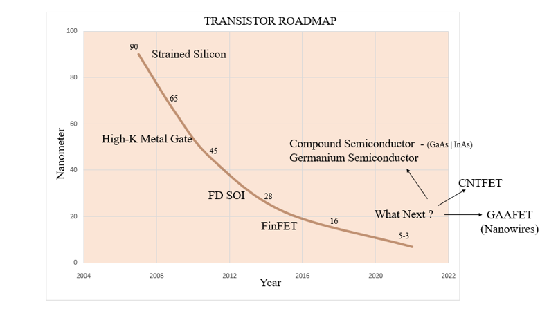
Nearly 60 years after Richard Feynman delivered his celebrated talk, which became the foundation for nanotechnology [1], many of the milestones he envisioned have been achieved and surpassed. In particular, he discussed computing devices with wires 10 to 100 atoms in width. Today we are reaching the smaller end of that range for high-volume FinFET and 10nm class DRAM chips, and device manufacturers are confidently laying the roadmaps for generations of conductors with single atom scales.

While device shrinkage has continued apace, it has not been without consequences. As chip circuit dimensions dip into the atomic range, bulk semiconductor properties which allowed for relatively simple scaling are breaking down and atomic-level physics are beginning to dominate. At this scale, every atom counts. And when different isotopes of the needed atoms have significantly different properties, the ability to create isotopically pure materials (IPMs) becomes essential.

In this paper, we begin by discussing several examples of IPMs used in current high-volume electronics manufacturing:  the physics at play and the materials selected. With the near future in focus, we then look at coming applications which may also require IPMs. Finally, we look at the current supply of IPM precursors, and how this needs to be developed in the future.

What is an isotope?

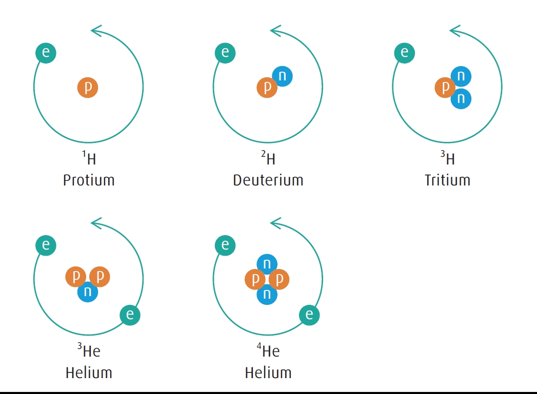
Isotopes are atoms of a particular element which have the same number of protons in their nucleus, but different numbers of neutrons (FIGURE 1). The number of protons determines which element the atom is:  hydrogen has one proton, helium has two protons, and so on in the ordering used for the periodic table.

FIGURE 1. The stable isotopes of hydrogen and helium. The number of protons determines the element, and the number of neutrons determines the isotope. The superscript number is the sum of the protons and the neutrons.

Different isotopes of the same element all have nearly exact chemical behavior – that is how they form and break molecular bonds in chemical reactions – but sometimes exhibit significantly different physical behavior. It is these differences in physical behavior which become important when electronics are made on the atomic scale.

For the purposes of engineering semiconductors, it is important to consider two different classes of isotopes.

  • Radioactive: The nuclei of these of these isotopes are unstable, break apart into different and lighter elements, and often emit radiation in the form of alpha particles or light. The rate at which this happens can be quite fast – much less than a nanosecond – to longer than a billion years for half of the material to undergo decay. It is this type of isotope which was first historically observed and which we often first learn about. The element uranium has five different isotopes which naturally occur on earth, but all of these are radioactive.
  • Stable: All other isotopes are termed stable. This means that they have not been observed to break apart, even once, when looking at bulk quantities of material with many billions of atoms. We do have evidence that some of these isotopes, termed primordial, are indeed stable over the span of knowable time, as we have evidence that they have formed and not decayed since the formation of the universe.

For the use of IPMs to engineer semiconductors, only stable isotopes are considered. Even for radioactive isotopes which decay slowly, the fact that current logic and memory chips have more than a billion transistors means that one or more circuits have the likelihood to be corrupted over the useful lifetime of the chip. In FIGURE 2, we show some common elements used in semiconductor manufacturing with their stable isotopes and naturally occurring abundances.

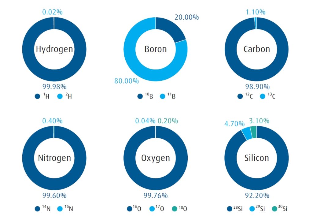
FIGURE 2. The natural abundance of stable isotopes for elements most relevant for electronics devices.

Current applications

There are already several electronics applications for IPMs, which have been used in high volume for more than a decade.

Deuterium (D2 = 2H2):  Deuterium (D) is the second stable isotope of hydrogen, with one proton and one neutron. As a material, it is most commonly used in electronics manufacturing as the IPM precursor gas D2. Chemically, deuterium can be substituted directly for any reaction using normally abundant hydrogen. Deuterium is made by the electrolysis of D2O, often called heavy water, which has been already enriched in the deuterium isotope.

Important physical property — mass:  For most elements, the difference in mass among their isotopes is only a few percent. However, for the lightest element hydrogen, there is a two-fold difference in mass. The chemical bond between a hydrogen atom and a heavier bulk material can be roughly approximated by the simple classical mechanics example of a weight at the end of the spring. When the weight is doubled, the force on the spring is also doubled (FIGURE 3).

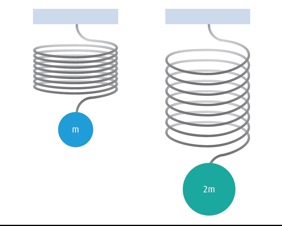
FIGURE 3. According to Hooke’s Law, a spring will stretch twice as far when attached to a mass twice the original. When the balls and springs are bonds to naturally abundant hydrogen 1H and deuterium 2H, they vibrate at different frequencies.

At the atomic level, quantum mechanics applies, and only certain amounts of energy, or quanta, can excite the spring. When deuterium 2H is substituted for the much more abundant 1H, the amount of energy which can excite the spring changes by almost 50%.

Long-distance optical fibers:  Optical fibers, like semiconductors, rely on silicon oxide as a primary material. The fiber acts as a waveguide to contain and transmit bursts of near-infrared lasers along the length of the fiber. The surface of the silicon oxide fiber is covered with hydroxide (oxygen-hydrogen), which is formed during the manufacture of the fiber. Unfortunately, the hydroxide chemical bonds absorb small amounts of the laser light with every single reflection against the surface, which in turn diminishes the signal. By substituting deuterium 2H for normally abundant hydrogen 1H on the surface hydroxide, the hydroxide molecular spring no longer absorbs light at the frequencies used for communication.

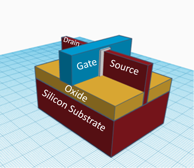
Hot carrier effect between gate and channel:  As transistor sizes decrease, the local electric fields inside transistors increase. When the local field is high enough, it can generate free electrons with high kinetic energy, known as hot carriers. Gate oxides are often annealed in hydrogen to reduce the deleterious effects of these hot carriers. But the hydride bonds themselves can become points of failure because the hot carriers have just the right amount of energy to excite and even break the hydride bonds. Just like in the optical fiber application, substituting deuterium 2H for naturally abundant 1H changes the energy of the bond and protects it against hot carrier damage. The lifetimes of the devices are extended by a factor of 50 to 100.

11-Boron trifluoride (11BF3):  Boron has two naturally occurring stable isotopes 10B at 20% and 11B at 80%. Boron is used in electronics manufacturing as a dopant for silicon to modify its semiconducting properties, and is most commonly supplied as the gases boron trifluoride (BF3) or diborane (B2H6). 11BF3 is produced by the distillation of naturally abundant BF3, and can be converted to other boron compounds like B2H6.

Important physical property – neutron capture:  The earth is continuously bombarded by high-energy cosmic radiation, which is produced primarily by events distant from our solar system. We are shielded from most of this radiation because it reacts with the molecules in our outer atmosphere. A by-product of this shielding mechanism are neutrons which constantly shower the earth’s surface, but are not strong enough to pose any biological risk, usually passing through most materials without reaction. However, the nucleus of the 10B atom is more than 1 million times likely to react with background neutrons versus other isotopes, including 11B. This results in splitting the 10B atom into a 7Li (lithium) atom and an alpha particle (helium nucleus) (FIGURE 4).

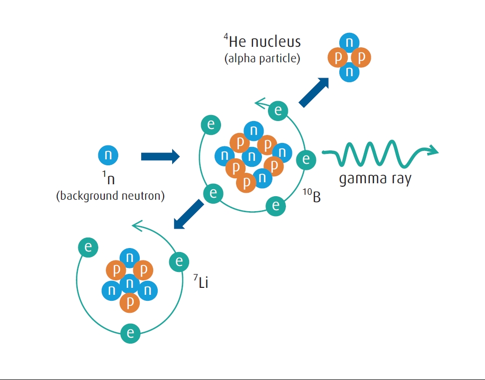
FIGURE 4. 10B neutron capture. When a 10B atom captures a background neutron, it breaks into a smaller 7Li atom and emits alpha and gamma radiation.

The smallest semiconductor gates now contain fewer than 100 dopant boron atoms. If even one of these is transmuted into a lithium atom, it can change the gate voltage and therefore the function of the transistor. Furthermore, the energetic alpha particle can cause additional damage. By using BF3 which is depleted of 10B below 0.1%, semiconductor manufacturers can greatly reduce the risk for component failure.

Initially, IPMs D2 and 11BF3 were used for making chips with the most critical value, like high performance computing processors, or remote operating environments like satellites and space vehicles. Now, as chip dimensions shrink to single nanometers and transistors multiply into the billions, these IPMs are increasingly being adopted into more high volume manufacturing processes.

Developing and future applications

As devices continue to scale to atomic dimensions and new device structures are developed to continue the progression of electronics advance, IPMs will play a greater role in a future where every atom counts. We present in this section a few of the nearest and most promising applications.

Important physical property – thermal conductivity:  Thermal conductivity is the property of materials to transfer heat, which is especially important in semiconductor chips where localized transistor temperatures can exceed 150 C and can affect the chip performance. Materials like carbon (either diamond or graphene) and copper have relatively high thermal conductivity; silicon and silicon nitride medium; and oxides like silicon oxide and aluminum oxide are much lower. However, with all of the other design constraints and requirements, semiconductor engineers seldom choose materials to optimize thermal conductivity.

When viewed in classical mechanics, thermal conductivity is like a large set of balls and springs. In an atomically pure material like diamond or silicon, all the springs are the same, and all the balls are nearly the same – the differences being the different masses of the naturally occurring isotopes. When IPMs are used to make to make the material, all the balls are now exactly the same, there is less disorder, and heat is transferred through the matrix of balls and springs more efficiently. This has been demonstrated in graphene to improve the thermal conductivity at room temperature by 60% (Figure 5), and other studies have shown a similar magnitude improvement in silicon.

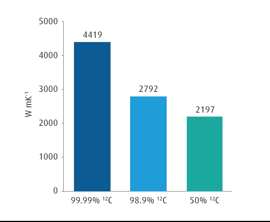
FIGURE 5. Thermal conductivity of graphene for different concentrations of 12C content. 99.99% 12C is achievable using commercial grade 12CH4 methane; 98.6% 12C is the value of naturally abundant carbon on earth; 50% 12C is an artificial mixture to demonstrate the trend. Source: Thermal conductivity of isotopically modified graphene. S Chen et al., Nature Materials volume 11, pages 203–207 (2012).

Silicon epilayers:  Epitaxially grown silicon is often the starting substrate for CMOS manufacturing. This may be especially beneficial for HD-SOI applications where trade-offs of substrate cost vs processing cost and device performance are already part of the value equation.

Sub 3nm 2D graphene FETs:  Graphene is a much-discussed material being considered for sub-3nm devices as the successor technology for logic circuits after the FinFET era. Isotopically pure graphene could reduce localized heating at the source.

Important physical property – nuclear spin:  Each atomic nucleus has a quantum mechanical property associated with it called nuclear spin. Because it is a quantum mechanical property, nuclear spin is measured in discrete amounts, and in this case half-integer numbers. Nuclear spin is determined by the number of protons and neutrons. Since different isotopes have different numbers of neutrons, they also have different nuclear spin. An atomically and isotopically pure material will have atoms with all the same spin.

Qubits and quantum computing:  Much research has been published recently about quantum computing as the successor to transistor-based processors. IBM and Intel, among others, have made demonstration devices, albeit not large enough for practical applications yet. The most promising near-term realization of quantum computing uses qubits – atomic two-state components—which store and transmit information via electron spin, which is a property analogous to nuclear spin, and can be affected by nuclear spin. Many of these early devices have been made with isotopically pure diamond (carbon) or silicon matrices to avoid disorder from having multiple values of nuclear spin in these devices.

12-Methane (12CH4):  Carbon is predominantly 12C, with about 1.1% 13C in natural abundance. A large demand already exists for 13C chemicals, primarily used as markers in studying chemical and biological reactions. 13C is produced primarily by the distillation of carbon monoxide (CO), and then chemically converted to other carbon-containing precursors like methane (CH4). At the same time 13C is produced, a large amount of 13C-depleted 12CO is produced, which serves as a less expensive feedstock for applications which require IPMs made from carbon.

28-Silane (28SiH4) and other silicon precursors:  There are no such large applications driving the production of isotopically pure silicon precursors yet. Currently, research quantities of silicon tetrafluoride (SiF4) are produced primarily by using gas centrifuges, and then converted into silicon precursors like silicon tetrachloride (SiCl4), trichlorosilane (SiHCl3), dichlorosilane (SiH2Cl2), and silane (SiH4). Distillation of one or more of these materials would be a less expensive option for larger-scale production.

Other IPM precursors already exist for oxygen and nitrogen compounds, and are relatively inexpensive because they are also by-products from the production of chemical markers for less abundant isotopes. Aluminum and phosphorous only have one stable isotope, and so all compounds produced with these are isotopically pure in these elements.

Production methods

Production of IPMs is challenging because of the limited differences in physical and chemical properties normally used to separate and purify materials, and because of the low concentration of some of the desired isotopes. A number of creative approaches have been applied, and often the methods are repeated to obtain the desired enrichment and purity of the IPM. We give a description here of the two methods used today in the production of IPMs relevant to the electronics industry. Importantly, all of these require gas-phase starting materials in order to enhance the physical differences that do exist among the isotopes.

Distillation:  The more familiar of the two is distillation, which relies on differing boiling points of materials to separate them into lower boiling point fractions called lights (which often are lighter in mass) and higher boiling point fractions which are called heavies. Because the boiling point differences are a fraction of a degree, very long distillation columns are used. Distillation is best used with lighter compounds, and is the preferred method for producing D2O, 11BF3, 12CO / 13CO, and isotopes of nitrogen and oxygen (FIGURE 6).


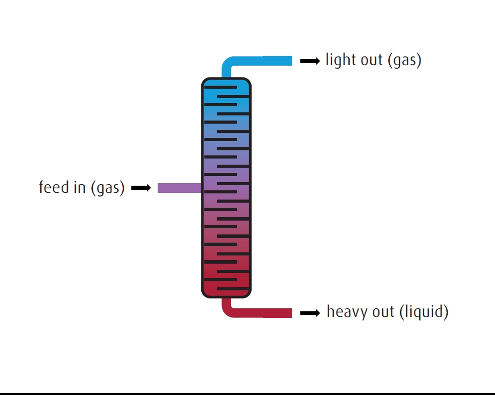
FIGURE 6. Isotope separation. Distillation. Gas is fed into the middle of the distillation column. By the process of condensation and boiling on many plates, the lighter isotope is separated as a gas leaving the top of the column, and the heavier isotope leaves as a liquid at the bottom.Centrifuge:  After a number of other methods were tried, gas centrifuges were the method ultimately chosen to scale the separation of the 235U uranium isotope in uranium hexafluoride (UF6) gas used for the first atomic devices during the Manhattan Project, and remains the preferred method of obtaining this useful isotope and other isotopes of heavier elements. The gas is spun at very high speeds – around 100,000 rpm – and the higher mass isotopes tend toward the outer regions of the centrifuge. Many gas centrifuges are linked in arrays to achieve the desired level of enrichment. Currently, useful quantities of of 28SiF4 and 30SiF4 are produced with this method (FIGURE 7).


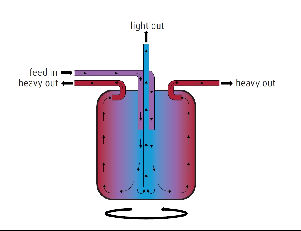
FIGURE 7. In this isotope separation centrifuge, gas is fed into the center of the centrifuge, which is spinning at a very high rate of 100,000 rpm. The heavier isotope is thrown to the sides, while the lighter isotope remains in the center.

Conclusion

In the hundred-year anniversary of Richard Feynman’s birth, we are still finding plenty of room at the bottom. But as we go further down, we must look more carefully at what is there. Increasingly, we are seeing that individual atoms hold the properties that are important today and which will support the developments of a not-too-distant tomorrow. IPMs are an important part of creating that reality.

Linde Electronics is the leader in the production of IPMs which are important to electronics today, and holds the technology to produce the IPMs which will support the development of tomorrow’s devices. Linde has made recent investments for the production of deuterium (D2) and 11BF3 to satisfy global electronics demand, and has a long history in the production, purification, and chemical synthesis of stable isotopes relevant to semiconductor manufacturing.

Reference

  1. Feynman, Richard P. (1960) There’s Plenty of Room at the Bottom. Engineering and Science, 23 (5). pp. 22-36.