Category Archives: 3D Integration

In a system-in-package (SiP) chip stack, space constraints can lead to large parasitic inductances in the packaging. Planarity, processing, high-temperature exposure, and other factors also present challenges. A new anisotropic conductive adhesive technology could enable low-cost flexible packaging via a multi-layer particle structure. S. Manian Ramkumar, Ph.D., RIT, reviews the adhesives benefits to various levels of electronics interconnect.

The electronics industry is continuing its push for product miniaturization and RoHS compliance through innovative component technologies, PCB assembly technologies, and materials. For portable consumer products like flash, MP3 players and heterogeneously integrated RF systems, chip stacking using a system in package (SiP) approach is becoming more popular. In these space-constrained applications, conventional packaging techniques become very complex, and result in large parasitic inductances. Other challenges such as planarity, extra processing steps, and high temperatures arise while using a bumping and flip chip bonding approach. These challenges have renewed the industry’s interest in exploring the use of electrically conductive adhesives (ECAs) for various applications at the component packaging level and also at the lead-free PCB assembly level.

A novel anisotropic conductive adhesive (ACA) is currently available in the market to address these challenges and provide a means for low-temperature flexible packaging. Referred to as the ZTACH ACA by its manufacturer, the novel ACA uses a magnetic field during thermal or UV curing to align the particles as columns in the Z-axis direction (Figure 1). This method of aligning the particles as columns eliminates the need for pressure during assembly, to capture conductive particles between the mating surfaces. Unlike a conventional ACA, more than one particle is typically captured between the opposing surfaces with ZTACH. The formation of conductive columns eliminates bridging between adjacent pads, and has proven to accommodate varying lead configurations. Modification of the filler size and filler proportion enables control of the column density, column spacing, and the required contact pad area for minimum resistance. The novel ACA also enables mass curing of the adhesive, eliminating sequential component assembly. The ZTACH ACA offers numerous benefits for SiP assembly, including thin form factor, low assembly cost, and low parasitic impedances for high data rate, high-frequency applications. Unlike traditional ACAs, ZTACH ACA has a low parasitic capacitance because of the multilayer-particle structure after curing.


Figure 1.

The ZTACH material is being researched at the Center for Electronics Manufacturing and Assembly (CEMA) at the Rochester Institute of Technology (RIT) and at the IDEAS lab at Purdue University. The novel ACA’s applicability for PCB-level assembly has been successfully demonstrated by RIT. The research at RIT has also characterized the base material properties, analyzed the effect of various process parameters, identified failures, and investigated the ACA’s long-term reliability for surface mount PCB assembly. Specific characterization and analysis carried out by RIT include process parameters such as print thickness, placement speed, pressure and dwell, cure temperature and time, magnetic field strength, substrate finish, component termination finish, and leaded or bumped packages of varying configurations. Reliability testing included an investigation of the assembly performance in temperature and humidity aging, thermal aging, air-to-air thermal cycling, and drop testing conditions. The IDEAS lab at Purdue University has been using ZTACH to successfully implement highly integrated RF SiP modules using novel concepts such as reverse pyramid stacking and nested chip stacking. The Purdue research has also demonstrated that chip-to-chip silicon wafer interconnects assembled by manually dispensing ZTACH, without any additional preparation for individual chip I/O pad bonding, show very good RF performance, up to 90 GHz.
 
Thermal aging of the novel adhesive material has revealed improvement in contact resistance. Area array packages, with and without bumps, have shown variations in performance and have revealed the importance of placement pressure, speed, and dwell in achieving low initial contact resistance. Area array packages with bumps have provided consistent performance with low contact resistance. A mathematical model has been developed to model the column formation and prove its validity with experiments. The research published by RIT also indicates that immersion silver (ImAg), electroless nickel immersion gold (ENIG), hot air solder leveling (HASL), and organic solderability preservative (OSP) finishes outperform immersion tin (ImSn) finish during temperature/humidity aging. The research by the Purdue group has demonstrated successfully the use of ZTACH to package Tx silicon board for biomedical applications, such as the study of glaucoma in rabbits and mice. Note that glaucoma is predicted to affect about 60.5 million people by 2010. Biomedical implantable micro-systems, used in the study of medical conditions such as glaucoma, require exceptional levels of integration (300 × 300 × 300 µm3) and low profile (<50 µm), along with bio-compatibility. These features make ZTACH suitable for the 3D packaging required in these applications.

1. ZTACH is a trademark of SunRay Scientific, www.sunrayscientific.com

S. Manian Ramkumar, Ph.D., is an SMT Editorial Advisory Board member and professor and director at the Center for Electronics Manufacturing and Assembly (CEMA) at Rochester Institute of Technology (RIT). Contact him at [email protected]; http://smt.rit.edu. In the discussion of the novel ACA’s properties, Dr. Ramkumar fully discloses that he holds a small equity stake in SunRay Scientific. The material properties discussed here were derived from unbiased university testing at RIT under fully established compliance procedures and Purdue and not influenced by the company.

Advanced Packaging, June 2010, http://www.electroiq.com/index/packaging.html

Also read:


The second wave of 3D packaging technology: PoP

PoP, together with WSP and QFN, have been the industry’s most successful packages during the last decade, and their success will extend into this decade. Mario A. Bolanos, Texas Instruments Inc.

Electroless NiAu on thinned wafers enables cost efficient prototyping

The electroless deposition of nickel and gold (ENIG) is a well established process for printed circuit board manufacturing; applied to electronic wafers, it offers a cost efficient under bump metallization for soldering, Ag sintering or gluing applications. Dirk Kähler, Fraunhofer Institute for Silicon Technology ISIT, Itzehoe, Germany


May 20, 2010 – High-density through-silicon stacking (TSS) shows promise for very high-volume applications, but work still needs to be done to "tame" key issues in manufacturing, improve costs, and smooth out the supply-chain, said Matt Nowak, director of engineering in Qualcomm’s VLSI technology group, in a presentation at The ConFab in Las Vegas.

High-density TSS refers to small diameter (~5μm), high aspect ratio (~10:1) via-middle through-silicon vias (TSV), used in backside wafer interconnect processing of high-density (10s of μm pitch) tier-to-tier microbump connections, with >1000s of TSVs and microbumps per chip. Though there is "industry momentum" for high-density TSS in very high-volume applications, work still needs to be done to "tame" issues with design, thermal management, manufacturing costs, and test — e.g. through "judicious system partitioning" to clarify design and manufacturing supply-chain handoffs. There also are a variety of manufacturing flow options to consider: die-to-die, die-to-wafer, die-to-substrate, wafer-to-wafer, etc. — also thin before/after stacking, bump before/after post-fab processing, and tier-to-tier attach techniques such as microbump and Cu-Cu.

Click to Enlarge
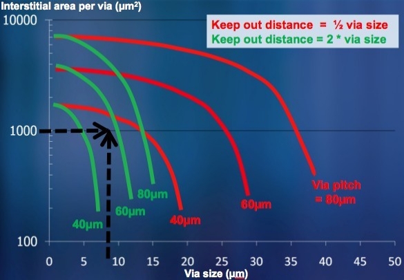
Via size, pitch, KOD, and required interstitial area impact silicon cost.

Cost in particular is currently a key challenge, he said, and there is no shortage of culprits, from incremental test cost to yield loss in both TSVs and microbumps, and incremental TSS process steps. Silicon area for TSVs is a key consideration as well, he pointed out, with via size, pitch, keep-out distance, and required interstitial area all impacting cost (see figure above). Possible cost-savings opportunities can be found in tweaking the laminate package size and number of layers, splitting large dies into two higher-yielding dies, and dividing into heterogeneous technology nodes.

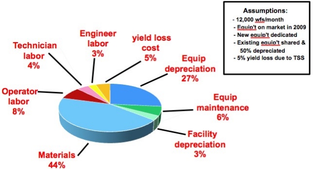
By far the biggest cost culprits are materials- & equipment-related, Nowak pointed out (see figure below). These can be addressed by improvements in materials (adhesives, underfill, molding compounds), equipment cost-of-ownership (throughput, uptime, tool configuration vs. volume), simplified process flow (e.g. eliminating B-RDL, replacing microbumps with lower-cost tier-tier bonding), and simplifying or eliminating temporary carriers.

Click to Enlarge

He also urged standards for supply-chain handoff points, with specs and test methods to reliably manufacture TSS from multiple sources and processes, validated by experimental results (reliability, cost, yield, etc.). Target areas for initial standards include:

  • Nomenclature/definitions
  • TSV size, tier thickness, via fill material
  • Tier-to-tier pin locations and assignments
  • Key physical design rules
  • Microbump and passivation materials properties and geometries
  • Reliability test methods
  • Metrology
  • Thin wafer shipping

Tony Flaim, CTO at Brewer Science, describes the work the company is doing to enable 3D integration. While progress is moving forward, he tells SST‘s Debra Vogler that end users are still somewhat unsettled in their choices of manufacturing technologies.

Emerging technologies, such as imbedding components within organic substrates, fulfill challenging electronics design objectives. Imbedded component/die technology* is a method of imbedding active and passives into cavities within a multi-layer printed circuit board (PCB) to decrease the surface area required to implement the circuit design and increase the robustness of the overall assembly. Casey H. Cooper, STI Electronics Inc., discusses the design methodology, packaging processes, and test data gathered during imbedded die/component packaging implementation in a mixed-signal prototype. The prototype was subjected to reliability testing and ultimately demonstrated in a test flight. Test results are provided here.

The electronics industry has seen an explosion in development of new materials and processes to support “smaller, lighter, faster, and better” products. Military and aerospace electronics providers continue to push the technological envelope, designing and manufacturing leading-edge high-reliability electronics. Current design problems are not caused by circuit design capabilities but by an inability to reliably package these circuits within the space constraints. Innovative packaging techniques are required to meet the increasing size, weight, power, and reliability requirements of this industry without sacrificing electrical, mechanical, or thermal performance.

Over the last decade, advanced packaging technologies have shifted to 3D integration.1 Whereas most new products have defined X and Y dimensions, added capability is left confined to integration within these boundaries, forcing engineers to rely on miniaturization that can only be achieved through smaller form and fit factor components and interconnection in the Z direction. Some established packaging technologies integrate bare die of both actives and passives into package designs, such as multichip modules (MCM), system-in-package (SiP), chip-on-board (COB), and emerging system-level designs such as imbedded components.2

In a paper presented at SMTA’s Pan Pacific Conference in 2004, the features and advantages of imbedding actives and passives were described.3 Since then, development was completed on an imbedded die manufacturing process,4 imbedding unpackaged components, i.e. bare die, for further electronics hardware miniaturization than current packaging technologies, such as SMT, cannot provide.

Packaging Technology

This embedded packaging approach addresses miniaturization, thermal management, performance, reliability, and system capability requirements through innovative design guidelines and materials selection. Elimination of external component packaging reduces circuit card assembly (CCA) size, weight, and electrical and thermal parasitics, and it enables the 3D assembly of multiple components. 3D assembly facilitates design integration of key subsystems, i.e. multiple CCAs, into a single high-density module.

Miniaturization is achieved fundamentally due to the elimination of external component packaging. Bare die enable designers to specify the smallest form and fit factor available. Component geometries can be reduced up to 85% through the removal of external leadframes, package substrates, and overmold encapsulants. These die are then imbedded in openings/cut-outs of the PCB, commonly referred to as cavities (Figure 1). Imbedding die in cavities in the substrate facilitates Z-integration through imbedding die on tiers, or exposed layers, within the substrate.

Figure 1. Active and passive components imbedded in a cavity on a laminate substrate.

With the free real estate on the PCB provided by reduced component footprints, additional systems or capabilities can be added to an electronics assembly. System capabilities can be increased through the integration of additional features and functionality and/or redundant system within the same envelope. For example, processing architectures, such as those implemented in field programmable gate arrays (FPGAs), may be easily scaled to increase the number of processing elements within the same PCB envelope due to component-level miniaturization.

Elimination of secondary packaging materials plays a significant role in overall weight reduction achieved through imbedding unpackaged die. Interconnect materials that physically and electrically connect the bare die integrated circuit (IC) to the circuit are eliminated. There is also a reduction in the mass related to the electrical interconnect material, achieved by using wire bonds rather than solder. Typical bonding wire alloys have a lower density than solder, and wire bonds use a significantly lower volume of material per connection.

End-product reliability is improved not only by a reduction in attachment material mass through the elimination of external component packaging, but also through the increased flexibility of the electrical attachment. By using wire bonding technology as the electrical attachment process, very flexible light-weight interconnects are created. This flexibility is exploited during operation in demanding thermal and mechanical environments such as high temperature, vibration, and/or mechanical shock. In contrast to a soldered connection, which localizes the applied stress, the imbedded package concept distributes the applied stress producing a more robust and rugged electrical product.

Embedding actives and passives into the PCB improves long-term signal reliability by eliminating unnecessary failure opportunities and utilizing reliable electrical interconnects. All first-level component packaging is eliminated. This reduces two to four possible modes of electrical failure associated with component-level packaging. Due to the removal of external packaging, electrical parasitics and thermal resistance are reduced, improving overall system performance. This means the assembly is suitable for high-speed, high-I/O electronics, such as those found in missile defense systems.

Conventionally, a high-power CCA would dissipate heat through convection or radiation from the component and substrate surfaces, often including package-level heat sinks or cooling fans. However, advanced handheld applications inhibit the use of active cooling devices such as large, finned heatsinks and fans. Imbedded die/component technology relies on passive cooling via conduction to a single, central cooling core to remove heat from high-power devices and to evenly distribute the thermal energy along the interface. Through creative thermal management, die junction temperatures (TJ) are reduced, increasing package- and system-level reliability.3

Prototypes

We recently completed testing of two prototype vehicles to provide a technology demonstration of the design guidelines, materials, and manufacturing processes used to imbed passive and active devices in laminate substrates. Environmental stress testing was conducted on these prototypes to evaluate the robustness of imbedded bare die in an organic laminate substrate in conventional military and aerospace environments, i.e. harsh environments.

Test vehicle 1. A test vehicle was designed to evaluate the effectiveness of assembly materials in harsh environments when imbedding bare die (silicon) in organic laminate substrates. The test vehicle consisted of multiple imbedded die (Figure 2) wired to inner layer tiers for monitoring fluctuations in resistance during/after environmental testing. The imbedded test die consisted of silicon, daisy-chain components with peripheral bond pads for interconnecting to a test substrate. Test patterns on the high-temperature FR-4 (HT-FR4) laminate substrate enabled in-situ resistance monitoring of the assembly during testing. A conformal coating, encapsulant, and lid were used (Figure 3) to protect the imbedded die from physical damage (handling/transportation) and environments (thermal movement due to coefficient of thermal expansion (CTE) mismatch, ionic contamination, and moisture ingression).

The test coupon comprised a 4.000 × 6.000″ HT-FR4 substrate, laminate PCB, in three tiers, with an imbedded copper core and Ni/Au plating. The Si die was 0.248 × 0.240″, daisy-chain design, with peripheral wire bond pads. The die attach material was thermally conductive, electrically insulative compliant epoxy. A 1.2-mil-diameter Al/1%Si wire formed each interconnect. Conformal coating was achieved with a 0.6-mil-thick parylene C material; encapsulation used silicone gel to a 95% cavity fill. The lid was laminate with top/bottom copper plane layer.

Figure 2. High-resolution images of test coupon daisy-chain die in the central cavity: upper left die (left) and lower left die (right).
Figure 3. High-resolution image of test coupon final assembly.

Materials properties found on the technical data sheets were reviewed prior to selection of die attach, conformal coating, and encapsulant candidates to include in the test matrix. Materials were identified that minimize CTE-induced stress on the devices and interconnects and to reduce the thermal resistance between the die junctions and substrate/heat sink. Certain characteristics are desirable for all materials comprising the assembly. Materials with a glass transition temperature (Tg) outside the operating environment range can minimize thermomechanical stresses induced by a material’s state change from glassy to rubbery. Die attaches, underfills, and encapsulants with low ionic contaminates minimize opportunities for corrosion in harsh environments. Materials’ thermal and electrical performance equally contribute to system-level performance requirements. Materials meeting the following specifications were selected to be included in the test matrix.

Critical material properties:

  • Cure temperature: The type of cure, snap cure versus a step cure, and cure temperature affect the cured material properties including Tg. The glass transition temperature should be significantly above the upper operating temperature range of the assembly to enable lower expansion/CTE of the material over a wider temperature range.5
  • Material purity: Low ionic contaminants and alpha particles emitted will aid in increasing the reliability of the bare die. Industry recommends chloride (Cl-), sodium (Na+), potassium (K+), and fluorine (F-) levels of less than 5 to 10 ppm to increase the die’s resistance to corrosion.6 Less than 0.001 particles/cm2/hr minimizes irradiating particles found in encapsulants that can cause soft errors in logic and high-density memory devices such as DRAMs and SRAMS.7
  • Voiding: Voids, or air pockets in the material, result in increased localized stresses, which can lead to premature delamination or loss of adhesion to the die and/or substrate. The material is no longer an effective stress buffer with voids present, and the material’s thermal resistance is increased due to air’s poor ability to transfer heat.
  • Moisture absorption: Due to use of organic substrate materials, a hermetically sealed assembly cannot be achieved, thus the materials selected should be hydrophobic  in nature.8
  • One-part system: One-part materials are easily integrated into the manufacturing and assembly process. All components of the material, curing agent, and hardener, are premixed ensure product uniformity and quality and eliminate operator errors. The material is supplied in a syringe for use on automated dispensing equipment and is typically stored at -40ºC to prevent changes in performance.

Thermal cycling fatigue or overstress failures are often detected through alternating exposure of the assembly to extreme temperatures with short transition times between extremes. The test vehicle was placed in a thermal shock chamber to evaluate the materials’ resistance to temperature excursions and the process parameters used to assemble the test vehicle. The assembly was placed on a tray that transitions from a cold chamber (air) to a hot chamber (air) within a specified time. Test conditions were changed periodically during the thermal shock test. Test conditions included: 1000 cycles from -55°C to 85°C, 250 cycles from -55°C to 125°C, 200 cycles from -55°C to 85°C, followed by 4200 cycles from -55°C to 125°C. The test vehicle was subjected to over 175 days of thermal shock cycling.

Critical materials evaluated during this analysis included:

  • Die attach adhesive: Determine effect of stress-related cracking of silicon die due to mismatch in coefficient of thermal expansion (CTE) of die and laminate/copper core.
  • Conformal coating: Determine aging characteristics of Parylene after repeated exposure to extreme temperatures.
  • Encapsulant: determine warpage and stress due to modulus and CTE differential of encapsulant and assembly (silicon die, laminate substrate, metal core, aluminum wire bonds).

Continuity testing was performed prior to cycling to establish a baseline resistance for each of the daisy-chains and at periodic intervals to monitor resistance fluctuations. Five daisy-chain die were imbedded within the test coupon, providing 30 daisy-chains, equivalent to 60 wires (120 wire bonds), for monitoring. A 3.0? increase in resistance constituted a failure with the cycles-to-failure data noted in Table 1. The first failure/high-resistance bond occurred after exposure to 3000 cycles with a lapse of 1500 cycles till the second noted failure. Only 23% of the wires failed after 5500 cycles when the test coupon was pulled from cycling.

Table 1. Thermal shock failure data for daisy-chain wires.
Daisy-chain wire group  Cycles  Wire Group  Cycles
3,057  16  none
4,507  17  none
4,507  18  none
4,947  19  none
5,102  20  none
5,656  21  none
5,656  22  none
none  23  none
none  24  none
10  none  25  none
11  none  26  none
12  none  27  none
13  none  28  none
14 none  29  none
15  none  30  none

The failure data gathered from this test vehicle indicates that the material properties selected will provide the long-term reliability solution for critical military electronics hardware. Compliant die attach adhesive enables stress relief from thermal-induced stress in the silicon-die-to-substrate interface while the wire bonds, coupled with a compliant encapsulant, provide the stress relief from environmental-induced stress (thermal, shock, and vibration). This material set, in conjunction with the imbedding design guidelines, enables robust, reliable electronics assemblies.

Test vehicle 2. A mixed-signal test vehicle (Figure 4) was designed and assembled to serve as a technology demonstration for the Navy’s Standard Missile-2 (SM-2) program. The Navy’s SM Program Office used this prototype in a flight test to support a technology demonstration of the imbedded component/die technology, validating the electrical and mechanical performance. A prototype was designed with a mix of analog and RF circuitry using imbedded design practices with wire-bondable devices. The prototype circuit design was selected to address miniaturization, thermal dissipation, component obsolescence, and reliability.

Figure 4. Mixed-signal prototype to demonstrate IC/DT packaging technology’s capabilities.

Miniaturization objectives were largely achieved due to the ability to locate wire-bondable components for the circuit. All ICs were procured as unpackaged components (wire bond/face-up die), and passives with gold metallization were procured for imbedding into the prototype. Through elimination of the secondary packaging, a 66% reduction in surface area was achieved. This reduction enables the integration of future CCAs into a single assembly module (increased form, fit, and function through added capability within the same footprint).

All components, both actives and passives, were imbedded into cavities (Z direction) in the laminate substrate. Multiple tiers were exposed in the substrate with strategic placement of components to decrease interconnect length (component-to-component bonding and component-to-substrate bonding) and address power dissipation. Bonding high-power devices with thermally conductive adhesive directly to an imbedded thermal core in the substrate eliminates the need for external heat sinks and lowers the devices’ junction temperature.9

Flexible aluminum wire bonds (Figure 5) were used to electrically interconnect the devices (component-to-component for point-to-point) and circuit (component-to-substrate for multi-point nodes). These flexible interconnects are able to absorb the thermal and mechanical stresses created when operating in harsh environments. Elimination of secondary packaging, which facilitates bonding from component-to-component, also decreases the number of failure opportunities in the system.

Figure 5. Wire bonds to electrically interconnect components on the prototype.

The prototype was analyzed and tested by SM-2 prime contractor Raytheon Missile Systems, which approved the prototype as flight hardware for a flight test. This included finite element analysis (FEA) design modeling and prototype qualification testing per standard legacy performance requirements and overstress test requirements (e.g. temperature, humidity, vibration testing). In October 2007, the prototype’s performance and robustness were demonstrated through a successful SM-2 flight test. The imbedded product was given TRL 8 status, meaning that the technology has been proven to work in its final form and under expected conditions. Examples include developmental test and evaluation of the system in its intended weapon system to determine if it meets design specifications.10

Materials Analysis

Materials analysis was performed on the prototype to determine the effects of performance qualification and overstress testing on the prototype units. A cavity was removed from the prototype to perform surface and micro-section analysis of the physical (die attach and conformal coat) and electrical (bond wires) interconnects. Prior to surface analysis, an aggressive organic solvent removed the encapsulant from the cavity to enable visual analysis of the various surfaces (through the conformal coating).

A scanning electron microscope (SEM) exposed the component/substrate topology and wire interfaces. The backscattered electron imaging mode provided a high-magnification grayscale digital image of the device (Figure 6 and Figure 7). At high magnification, the substrate bond interfaces and die bond interfaces were inspected for signs of fatigue and stress fractures. However, the conformal coating remained over the die and wire surfaces, creating a monochromatic image around the components, bond wires, and substrate. Within this cavity, multiple component geometries and wire profiles are represented as well as multi-tier component placement (cavity within a cavity).

Figure 6. Micrograph SEM image (fisheye mode) of cavity with imbedded components and bond wires.
Figure 7. Micrograph SEM image of cavity-within-a-cavity (to thermal core) with imbedded components and bond wires.

The cavity was then micro-sectioned to analyze component-to-substrate interfaces and bond wire interfaces. The component-to-substrate interface directly affects physical attachment of the device to the substrate (and also electrical connects IC bulk silicon potentials to the corresponding voltage, as required) and is critical to withstanding cyclic thermal stress and shock/vibration. The bond wire interfaces are paramount to function and performance of the circuit where any stress fractures or lifts directly affect contact resistance and can lead to high resistance connections (open).

The component-to-substrate interface (Figure 8) is continually stressed due to the significant difference in CTE of the substrate bond pad (laminate = 16-20ppm/°C, copper = 16 ppm/°C, and aluminum = 24 ppm/°C) and the low CTE of electrical devices (ICs: silicon = 3 ppm/°C, Passives: ceramics = ~6 ppm/°C). Many parameters should be considered in calculating the induced stress (per Hooke’s Law) in a component-to-substrate interface. A designer has little control over certain parameters (component CTE, ΔT, dimensional parameters), but proper selection of the die attach adhesive (modulus, CTE, Tg) can significantly reduce interfacial stresses. Micro-section analysis of one such interface revealed no delamination (separation of materials) or stress fractures between the component-to-die attach interface or substrate-to-die attach adhesive interface.

Figure 8. SEM micrograph of component-to-substrate interface with thin bond line thickness to decrease thermal resistance.

The bond wire interface (Figure 9) is also affected by CTE differences in substrate and component bond pad materials (thermal stress), in addition to use environment stresses such as vibration and shock. The use of flexible interconnects, such as aluminum/1%silicon wire, prevent stress fractures in the electrical connect due to expansion and contraction of the devices and substrate during cyclic temperature changes. However, repeated wire flexing (such as during multiple thermal shock cycles) can lead to failures. Preventive measures such as conformal coatings and encapsulants and bond parameters (such as loop height) can prevent failures related to thermal expansion.

Figure 9. SEM micrograph of a silicon die bond pad-to-wire (Al/1%Si) interface.

These preventive materials and process parameters also aid in eliminating wire failures due to vibration and shock. Low-stress encapsulants act as a shock absorber to reduce the amount of force transferred to the wire when exposed to mechanical shock and vibration. Reduced wire lengths and controlled loop heights (Figures 10 and 11) also prevent fatigue and breaking by altering the resonant frequency of the wire bond.11

Figure 10. SEM micrograph a low-profile bond wire (step down from die to substrate) with first bond on the die surface. No lifts or fatigue cracks along the interface.

Figure 11. SEM micrograph a low-profile bond wire (step down from die to substrate) with second bond on the substrate. No lifts or fatigue cracks along the interface.

Wire bonding electrical interconnects versus conventional processes such as soldering provides significant flexibility in interconnecting miniaturized components in odd form factor packages where access to create these interconnects is restricted. High power devices located in recessed cavities for improved heat transfer (bonded to an imbedded cooling core) limit access to the die surface. Configurable bonding parameters enable access to the die bond pads in these locations (Figure 12).

Figure 12. SEM micrograph of a die bonded to the thermal core (deep access) in a recessed cavity. No lifts or fatigue cracks along the interface.

Like any metallurgical interface, intermetallic compounds are formed and are subject to failure. For bond wire interfaces, the classical failure mode is Kirkendall voiding which is often referred to as the “purple plague”. The failure mode is a function of several parameters: metallurgical interfaces (wire and pad metal composition), metal impurities, ion diffusion rates (aluminum diffuses more rapidly into gold), and environment (time and temperature). The term “purple plague” is derived from the characteristic color of one of the five intermetallic compounds that is formed at high temperatures (above 150°C) over time in gold/aluminum (Au/Al) compounds (such as Au ball bond to Al bond pad). The intermetallic layers are more brittle than either Al or Au and are prone to crack during temperature cycles or stresses. Therefore, the room temperature wire bonding process using ultrasonic wedge bonds (Al/1%Si wire) is preferred due to the bonding method (ultrasonic bonding is room temp versus high temp thermosonic bonding) and metallurgical interfaces (die bond pad-to-wire: Al-Al and passive bond pad-to-wire: Au/Al).11 Due to the overstress testing performed on this prototype, bond interfaces were inspected at high magnification for indication of fatigue cracks at the Au/Al interfaces (Figure 13). No voids or fatigue cracks were detected in the Au/Al interfaces, e.g. passive end termination-to-wire or substrate bond pad-to-wire.


Figure 13. SEM micrograph a gold-plated capacitor end termination bond wire. No voids or fatigue cracks were detected along the interface.

Conclusion

The testing of the two test vehicles has demonstrated that imbedding components and die is a robust packaging technology for use in products that must operate in harsh environments. The two test vehicles discussed in this paper have proven that the design guidelines, materials, and process parameters used to manufacture imbedded package assemblies are capable of withstanding temperature, humidity, and shock stresses. Test Vehicle 1 (daisy-chain sample) survived over 3000 cycles of thermal shock exposure before a failure occurred. Test Vehicle 2 (mixed-signal prototype) was bench tested to meet and exceed legacy product performance specifications in order to qualify the prototypes as flight hardware. Lastly, a successful flight test in October of 2007 was paramount in demonstrating imbedded component packaging technologies’ ability to meet form, fit, and function requirements in a miniaturized robust package.

*The packaging technology described here is registered by STI as Imbedded Component/Die Technology (IC/DT).4

ACKNOWLEDGEMENTS
The findings of this study could not have been accomplished without the support of the STI Microelectronics Lab and the STI Analytical Lab under the direction of Mark McMeen. The author would like to acknowledge the efforts of Jonnie Johnson and David Robinson for support of the design, assembly, and test of the prototype assemblies as well as Aaron Olson and Bryan McMeen for the post-stress testing sample preparation and analysis.

REFERENCES
1. Greig, Bill, “New and Emerging Technologies,” Advanced Packaging, July 2002.
2. Cooper, C. and McMeen, M., “Effects of Process Parameters on the Material Characteristics of Die Attach Adhesives,” Pan Pacific Microelectronics Symposium, January 2007.
3. Hatcher, Casey, “Imbedded Component/Die Technology: An Innovative Packaging Solution for High Reliability,” Pan Pacific Microelectronics Symposium, February 2004.
4. Raby et al. "Imbedded component integrated circuit assembly and method of making same." U.S. Patent 7,116,557. 3 October 2006.
5. Naito, C. and Todd, M., “The effects of curing parameters on the properties development of an epoxy encapsulant material,” Microelectronics Reliability, Vol. 42(1), pp. 119-125, 2002.
6. Gilleo, K., “Introduction to Material Science: Polymers and Fillers,” W-25: Conductive Adhesives Workshop – APEX Conference, March 2003.
7. Wong, C.P. “Polymers for encapsulation: Materials Processes and Reliability,” Chip Scale Review, March 1998.
8. Virmani, N.V. and Shaw, J., “Critical Concerns, Solutions and Guidelines for Use of Plastic Encapsulated Microcircuits for Space Flight Applications,” Retrieved October 4, 2006, from the NASA, Technology Validation Assurance Web Site: http://misspiggy.gsfc.nasa.gov/tva/pems/esapems.htm
9. Santarini, Michael, “Thermal Integrity: A Must for Low-Power-IC Digital Design”, EDN, September 2005.
10. “Appendix B: Technology Readiness Level (TRL) Descriptions”, NASA SBIR Website: http://sbir.nasa.gov/SBIR/sbirsttr2007/solicitation/appendix_B.pdf
11. Harman, George, “Wire Bonding in Microelectronics: Materials, Processes, Reliability, and Yield,” New York, NY: McGraw Hill, 1997.

Casey H. Cooper, STI Electronics Inc., Madison, AL, may be contacted at [email protected].

Advanced Packaging, April 2010

by Debra Vogler, senior technical editor, Solid State Technology

March 29, 2010 – As semiconductor industry evolves from planar scaling to 3D design to enable shorter interconnect lengths and higher I/O density along with more functionality, Applied Materials’ new Producer InVia dielectric deposition (CVD) system targets via-first and via-middle through-silicon via (TSV) integration applications. The new technology enables the deposition of the oxide liner film layer in high-aspect ratio (HAR) TSV structures.

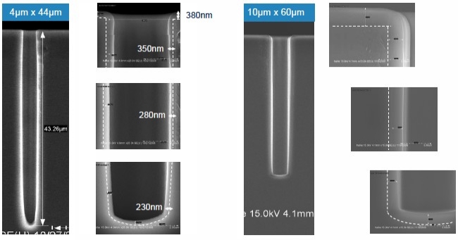
Because the via-middle application requires complete electrical isolation for device integrity, it has a thermal budget requirement ≤400°C, with conformality >50% of field oxide thickness over the full depth of the via (up to 11:1 A/R), sidewall thickness in the range 200nm to 1μm, and leakage current <2nA/cm2, among other requirements (see Figures 1 and 2). According to Applied’s global product marketing manager, Kedar Sapre, 80% of the company’s customers are doing a via-middle application, which, he notes, offers the greatest flexibility.

Click to Enlarge
Figure 1. Coverage capability of the Applied InVia. (Source: Applied Materials)

The new dielectric liner solution is implemented on Applied’s Producer GT platform, which the company says has the capability to process up to 8× more wafers/hr at less than half the cost, particularly when depositing very thick liners.

Click to Enlarge
Figure 2. Conformality shown as aspect ratio vs. via opening. (Source: Applied Materials)


(March 9, 2010) SAN JOSE, CA — Novellus Systems (NASDAQ: NVLS) created an advanced copper barrier-seed physical vapor deposition (PVD) process for the emerging through-silicon-via (TSV) packaging market. The process uses Novellus’ established INOVA platform with patented hollow cathode magnetron (HCM) technology to produce highly conformal copper seed films that are reportedly four times thinner than the conventional PVD seed approaches used for other TSV applications. Novellus announced that the HCM TSV process delivers excellent sidewall and bottom coverage, and enables void-free copper fill during the subsequent TSV electroplating step.

In contrast to the traditional 2D pin-based chip packaging approach, TSVs enable multiple chips to be stacked on top of each other into one 3D module. The 3D stacked chips are connected to each other with short TSV copper interconnects that result in increased device speed and lower power consumption.

TSV copper interconnects utilize a conventional damascene deposition sequence of PVD copper barrier-seed followed by electrochemical copper fill to create the pillars that connect one chip to another. As compared to a traditional, dual damascene copper interconnect scheme, a TSV feature is extremely deep, in some cases up to 200 microns. This high aspect-ratio structure makes the deposition of conformal seed layers very challenging. Non-conformal copper seed layers have minimal sidewall coverage, and can lead to void formation during the subsequent copper TSV fill step, directly impacting device reliability. Conventional TSV integration sequences have addressed this issue in several ways. One method is to “relax” the aspect ratio of the feature by tapering the TSV etch process to create vias with non-vertical sidewalls. While this increases the subsequent PVD step coverage, it limits the ultimate packaging density that can be achieved. Another method is to deposit a thicker copper seed layer to achieve sufficient sidewall coverage within the TSV feature, although this results in an expensive manufacturing process due to higher cost of consumables and lower system throughput.

Novellus engineers have developed an HCM-based advanced copper barrier-seed process for TSV applications that addresses both the technical challenges and high manufacturing costs associated with the conventional approaches. The innovative technology uses a patented ring of permanent magnets within the PVD process chamber to create a strong, locally ionized field, which results in an increased ion density on the sidewalls of the TSV structure. Increasing the ion density in this region causes a larger fraction of the sputtered film to land on the sidewall, which in turn results in a more conformal deposition. This highly conformal process eliminates the need for tapered sidewalls and allows the deposited film thickness to be four times thinner than the typical PVD seed layers used for TSV applications. As shown in Figure 1, Novellus’ advanced seed process can achieve void-free feature fill in a 60 micron deep, 10:1 aspect ratio TSV feature with vertical sidewalls using a 2000 angstrom thick copper seed layer. The conventional PVD approach requires an 8000 angstrom thick seed layer to achieve the same result. The 4X thinner TSV seed layer results in a substantial increase to system throughput and reduces the cost-of-consumables by greater than 50 percent as compared to conventional PVD approaches.

“TSV 3D technology holds great promise for advanced semiconductor packaging applications, assuming that both the technological and productivity challenges can be addressed,” said Fusen Chen, Ph.D., Novellus’ executive VP of semiconductor systems products. “Novellus’ new advanced seed process addresses both of these challenges for the copper barrier-seed portion of the TSV integration sequence, resulting in a thin, highly conformal film with exceptional PVD system throughput to meet the needs of high-volume manufacturing.”

For copper barrier-seed applications, Novellus’ INOVA NExT PVD system features a patented HCM IONX source technology, providing highly conformal barrier films and scalable seed layers. Novellus Systems, Inc. (Nasdaq: NVLS) is a provider of advanced process equipment for the global semiconductor industry. www.novellus.com


March 2, 2010 – Allvia says it has integrated embedded capacitors on silicon interposers, a key interface between silicon devices and organic substrates, achieving >1500nF/cm2 capacitance.

Thin-film capacitors without through-silicon vias (TSV) have been used, but high interconnect inductance prevents their full benefit, the company explains. 3D integration with TSVs allows a much closer electrical path between the device and power supply decoupling capacitors; thus the low inductance TSV interconnects enable very high electrical performance when integrated with embedded thin-film capacitors, the company explains.

The company earlier this year announced integration and reliability testing of a silicon interposer between semiconductor die and substrate using its TSV technology.

Allvia CEO Sergey Savastiouk noted that with this process, capacitance from the die or package can be transferred to the interposer — and that the 1500nF/cm2 capacitance value "is not a limit of our process."

by Thorsten Matthias, Markus Wimplinger, Paul Lindner, Bioh Kim, Eric Pabo, Dustin Warren, EV Group

Executive overview
The advantages as well as the technical feasibility of through-silicon vias (TSV) have been acknowledged by the industry. Today, the major focus is on the manufacturability and on the integration of all the different building blocks for TSVs and 3D interconnects. In this paper, the advances in the field of lithography, thin wafer processing and wafer bonding, are presented, with an emphasis on the integration of all these process steps.

Copyright © 2009 by International Microelectronics And Packaging Society (IMAPS). Permission to reprint/republish granted from the 42nd International Symposium on Microelectronics (IMAPS 2009) Proceedings, pg. 563-568, November 1-5, 2009, San Jose McEnery Convention Center, San Jose, California. ISBN 0-930815-89-0.

March 1, 2010 – Face-to-back integration schemes require the processing of thin wafers for both wafer-to-wafer and chip-to-wafer stacking. Prior to thinning, the device wafer is mounted on a carrier wafer with a temporary wafer bonding step. 300mm wafers with a thickness of 30μm have been successfully processed through the complete TSV process line.

Lithography on the backside of the thin device wafer requires alignment of the photo-mask to the alignment keys buried in the bond interface. After backside processing, the thin wafer is debonded from the carrier wafer. The thin wafer is either mounted on dicing tape for singulation and subsequent chip-to-wafer stacking, or it is bonded immediately to another device wafer for wafer-to-wafer stacking.

Click to Enlarge
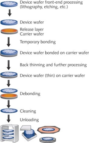
Figure 1. Process flow of thin wafer processing by temporary bonding and debonding.

For applications with very high TSV density, face-to-face integration schemes using Cu-Cu thermo-compression wafer bonding are a promising approach as the electrical contacts are established in parallel to the mechanical bond. Alternatively, fusion bonding is very attractive due to the cost-of-ownership advantages compared to metal-metal bonding. Recent equipment and process improvements enable sub-micron alignment accuracy on 300mm wafers.

3D integration and TSVs

Extensive research and development activities over many years have shown the feasibility as well as the technical advantages of through-silicon vias (TSV) and 3D integration. Many different manufacturing and integration schemes are being discussed and evaluated. Most or all of the individual process steps and building blocks have been successfully qualified. Today, industrial consortia such as EMC-3D focus on cost competitive manufacturability and on the integration of all the different building blocks for TSVs and 3D interconnects.

Vertical or 3D stacking of chips can be realized as chip-to-chip (C2C), chip-to-wafer (C2W) and wafer-to-wafer (W2W) manufacturing. The stacking of the chips itself can be realized as face-to-face or face-to-back integration [1]. Face-to-back integration requires wafer thinning and processing of the device wafer on the front- and backsides prior to permanent bonding of the dies or wafers.

Thin wafer processing

The ongoing demand for smaller and smaller devices requires minimizing the diameter of the TSVs. Although TSVs can be manufactured with quite extreme aspect ratios, the manufacturing costs are significantly lower for moderate or low aspect ratios of 1:5 up to 1:10. Therefore, small via diameters require thin device wafers.

Figure 1 shows the generic process flow for thin wafer processing with temporary bonding to a carrier wafer. The starting point is a device wafer with complete front-end processing on the frontside of the wafer. This device wafer is bonded to a carrier wafer with its frontside in the bond interface. After bonding the first step is back-thinning of the wafer. Usually, back-thinning is a multistep process consisting of mechanical back-grinding and subsequent stress relief etching and polishing. After back-thinning, the backside of the device wafer can be processed using standard wafer fab equipment. The carrier wafer gives mechanical support and stability and protects the fragile wafer edge of the thin wafer. Finally, when all backside processing is done, the wafer gets debonded, cleaned, and transferred to a film frame or to other output formats. Temporary bonding and debonding are enabling technologies for wafer-level processing of thin wafers. The main advantages of temporary bonding and debonding using a carrier wafer are compatibility with a number of processes and equipment, for example:

Standard fab equipment. The bonded wafer stacks literally mimic a standard wafer. The geometry of the bonded stack can be tailored in such a way that the resulting geometry is in accordance with SEMI. This brings the advantage that standard wafer processing equipment can be used without any modification. There is no need for special end-effectors, wafer chucks, cassettes, or pre-aligners. No downtime at all is required to switch between processing of standard thick wafers and temporarily bonded thin wafers.

Existing process lines. With the addition of only two pieces of equipment, the temporary bonder and the debonder, a complete process line or even fab becomes able to process thin wafers.

Existing processes. The mechanical and thermal properties of the bonded wafer stack are very similar to a standard thick wafer. This enables the use of existing wafer processing recipes, which have been proven and qualified for standard wafers.

Future process flows. The user has the full flexibility to change the processing sequence and the individual process steps for backside processing. After temporary bonding, the device wafer is securely protected against mechanical damage. Furthermore, adding process steps or modifying the process flow does not impact the cost of ownership for thin-wafer processing.

Product roadmaps. For many devices and products, the roadmaps lead to even thinner wafers in the future. With temporary bonding, the entire backside processing becomes independent of the wafer thickness. Reducing the wafer thickness does not require any modifications or adjustments to the processing equipment.

An important point is the choice of the carrier wafer. For silicon-based devices, the recommended carrier is a standard silicon wafer. First of all, with a silicon carrier, the resulting bonded stack mimics very closely a standard wafer. From a geometrical point of view, this enables the use of standard wafer processing equipment without modifications, whereas oversized carriers would require special wafer chucks and cassettes for the wafer stack.

Even more important are the thermal properties of the bonded stack. With a silicon carrier, the thermal expansion between device wafer and carrier is perfectly matched. Using a non-silicon carrier would cause the stack to bow and warp due to thermal expansion mismatch. There is the risk that the induced stress impacts the processing characteristics and ultimately the device performance. CTE-matched glass carriers create a different problem — metal ion contamination. It is not possible to use these glass carriers in CMOS fabs, which undermine one of the major advantages of the carrier wafer approach — the ability to process frontside and backside of the device wafer on the same equipment set.

Lithography for temporarily bonded wafers

For many integration schemes, after thinning and polishing, the backside of the thin device wafer has to be patterned with one or more mask levels. Due to the similarity between a bonded stack and a single wafer, standard spin coating and developing processes can be applied. Features such as bond pads, pillars, and bumps are typically created on a mask aligner. The exposure of the resist coated surface requires the alignment of the mask to the features on the device wafer front side, which is buried in the bond interface. Modern mask aligners have integrated IR alignment capability for this application (Figure 2).

Click to Enlarge
Figure 2. Front-to-backside lithography for a thin device wafer bonded to a carrier wafer. The alignment keys on the device wafer front side are buried in the bond interface. The alignment to the mask is performed with infrared (IR) alignment.


Permanent wafer bonding

There are three main wafer bonding methods for 3D interconnects: fusion (or molecular) bonding, adhesion thermo-compression bonding, and metal-metal thermo-compression bonding. In addition, there are hybrid methods such as simultaneous adhesive-metal bonding or simultaneous fusion-metal bonding. Each of these methods has advantages and disadvantages. Adhesion wafer bonding is not sensitive at all to particles; metal-metal thermo-compression bonding simplifies the process flow as the mechanical and electrical connections are established simultaneously in one process step [1].

Fusion wafer bonding is a two-step process consisting of room temperature pre-bonding and annealing at elevated temperature. The classical annealing schemes, which were developed for SOI wafer manufacturing, require annealing temperatures in the range of 800-1100°C. A surface pre-processing step, LowTemp plasma activation, enables the modification of the wafer surface in such a way that the annealing temperatures can be reduced to 200-400°C. Therefore, this type of plasma activation enables the use of fusion wafer bonding for 3D integration.

Fusion wafer bonding brings several advantages:

Alignment accuracy. By bonding at room temperature, bonding misalignment based on thermal expansion of the wafers is eliminated completely. Figure 3 shows alignment results with the EVG SmartView NT Aligner.

Click to Enlarge
Figure 3. Alignment results with the EVG SmartView NT Aligner: 400 alignments

Due to the very good alignment accuracy, fusion wafer bonding is especially well suited for high density TSV devices. The ITRS roadmap for high density TSVs specifies via diameters of 0.8-1.5μm in 2012 [2]. Sub-micron post bond alignment accuracy is necessary for these devices.

Throughput. Fusion wafer bonding has the highest throughput compared to adhesive or metal-metal thermo-compression bonding because it is a room temperature process. It can be implemented either as an in situ bond process in the aligner module or as an ex situ process under vacuum in a bond module. The subsequent annealing can be performed as a batch process in a furnace or oven.

Inspection capability after pre-bonding prior to final annealing. After the room temperature pre-bonding step, the bond strength is sufficiently high to enable inspection of bond quality and alignment accuracy. In case of misalignment or bond quality problems, e.g., voids, the wafer pair can be separated and reworked. This concept of inspection and, if necessary, reworking prior to final annealing has been used in SOI wafer manufacturing for many years.

Cost-of-ownership. The combined effects of in situ bonding in the aligner module, highest throughput, increased yield due to the ability to rework and reduced capital costs results in low cost-of-ownership for manufacturing schemes based on fusion wafer bonding.

The primary challenges for fusion wafer bonding are the sensitivity to particles and the specifications for surface roughness. Any particle within the bond interface will create an un-bonded area, a void. The size of the void can be up to 1000 times larger than the particle itself. A void in the bond interface will not only damage the directly impacted dies, but it may even prevent back thinning and thereby cause loss of the entire wafer. To overcome this threat, modern wafer bonding systems include wafer cleaning modules within the bonding platform. This equipment configuration enables cleaning of the wafer surface immediately prior to wafer bonding. Because of the integrated cleaning modules and the ability to rework the bonded wafers, the sensitivity to particles is no longer perceived as an issue for high-volume manufacturing.

Fusion wafer bonding requires surface micro-roughness in the range of 0.5-1nm. These requirements can be met with modern CMP technology.

Bond alignment inspection

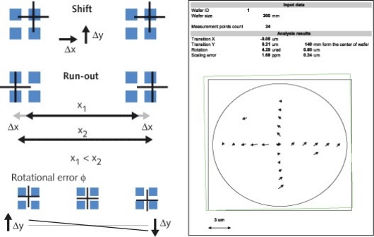
Post-bond alignment inspection is a critical process control step. A misaligned wafer bond can result in total loss of two fully processed wafers. Therefore, it is important to analyze all the contributing factors to the alignment accuracy. Figure 4 shows the different factors contributing to misalignment, as well as the process control output format for a bond alignment inspection system.

Click to Enlarge
Figure 4. Left side: Potential alignment errors: shift, rotational misalignment and run-out; the post-bond alignment is often an overlay of all three types. Right side: The post bond alignment inspection system EVG40 NT allows customer defined wafer mapping.

Conclusion

In this paper, significant improvements in manufacturing processes and equipments have been presented. Thin wafer processing is becoming a mainstream process. Temporary bonding to a carrier wafer, thinning, backside processing and subsequent debonding have been qualified for several different process flows. Using a silicon wafer enables the use of standard fab equipment for thin wafer backside processing. The SmartView NT aligner allows alignment accuracy in deep sub-micron range. Fusion wafer bonding has some unique advantages for 3D integration namely alignment accuracy and throughput. Process control including post bond alignment inspection is critical for improved yield and cost-of-ownership.

Acknowledgments

LowTemp and SmartView are registered trademarks of EV Group.

References
[1]. P. Garrou, C. Bowers, P. Ramm (Eds.), "Handbook of 3D integration," Wiley, 2008.
[2]. www.itrs.net

Biography

Thorsten Matthias is director of business development at EV Group, Erich Thallner Strasse 1, 4782 St. Florian/Inn, Austria, e-mail: [email protected].

(February 8, 2010) MASSY, France and ANSAN-CITY, South Korea — In a deal that will generate economical new process options for the 3D integration market, Alchimer S.A., a provider of nanometric deposition technology for semiconductor interconnects and through-silicon vias (TSV), and KPM Tech Co. Ltd., a manufacturer of plating materials and systems, announced a multi-level collaboration that gives KPM Tech exclusive rights to produce chemicals in Korea for Alchimer’s technology. The agreement also includes the manufacture of various configurations of wet processing tools to support the Alchimer TSV platform.

Alchimer’s Electrografting (eG) technology is an electrochemical-based process that enables the growth of high-quality polymer and metal thin films on both conducting and semiconducting surfaces. Alchimer’s deposition technology reduces overall cost of ownership for high aspect ratio TSV metallization by up to two-thirds compared to conventional dry processes, while shortening time to market.

“This agreement enables several key next steps in Alchimer’s transition into volume production environments, and also gives Alchimer a strategic presence in South Korea, which accounts for half the world’s memory production and will offer convenient access to our Asian customers,” said Alchimer CEO Steve Lerner. “This is a logical, strategic partnership that will enable us to apply our existing manufacturing infrastructure for chemicals and coating systems, while substantially expanding our available market,” said Chae Chang-Geun, CEO of KPM Tech.

Alchimer develops and markets chemical formulations, processes and IP for the deposition of nanometric films used in both semiconductor interconnects and 3D through-silicon vias (TSVs). The company’s breakthrough technology, Electrografting (eG), is an electrochemical-based process that enables the growth of very thin coatings, of various types, on both conducting and semiconducting surfaces.
                                                                    
KPM Tech Co., Ltd. manufactures surface treatment chemicals and automated plating systems for a variety of industrial uses.

Subscribe

Become a Fan on Advanced Packaging‘s Facebook Page

(January 22, 2010) MINNEAPOLIS — The Surface Mount Technology Association (SMTA) will host two 90-minute online sessions with Bob Willis, ASKbobwillis.com, on package-on-package (PoP) applications and implementation. The Webtorials will take place February 4 and February 11, 2010 from 1:00 to 2:30 pm EST.

PoP applications are growing in popularity for mobile and handheld professional electronics applications, placing further demands on assembly engineers. In simple terms, POP represents the stacking of components one on top of another either during the original component manufacture or during printed board assembly. As real estate is at a premium for logic and memory, PCB designers say the only way to go is up and up. PoP packaging systems may include direct soldering, wire bonding, or conductive adhesives for device to device interconnection.

PoP is new to many contract and OEM assembly staff but with the demands of paste dipping, reflow warpage, increased placement accuracy/Z-axis control process introduction can be demanding. The difficulty in multi-level ball inspection can be a challenge for X-ray equipment procedures as level one balls can mask level two and three interconnections. Manual inspection can be used but with these applications space is often not available for side viewing. Each delegate will receive a free set of package on package inspection and quality control wall charts covering optical and X-ray inspection, dip flux and paste application, placement criteria and defects seen during assembly.

This webtorial suits design, production and quality engineers looking at future technology and maintaining a company technology roadmap. It’s vital to subcontractors to be up-to-date with new technology and its possible implementation along with material and equipment requirements for future customers.

Topics include:
What is Package on Package (PoP)?
Benefits of PoP Stack Packages
Component Standards
Component Types
JEDEC Standards
PCB Design Rules
Pad Layout
Via Hole Connection
Lead-Free Assembly
Engineering Interviews
Stencil Printing
POP Placement 
Tack Flux
Dip Solder Paste
Reflow Soldering
Convection
Vapor Phase Soldering
Temperature Profiling
Inspection
Optical Inspection
X-ray Inspection

Underfill
Rework
Package on Package Defects
 
Bob Willis currently operates a training and consultancy business based in England with a large collection of interactive training CDs. A specialist in implementing lead-free manufacture, Willis provides worldwide training and consultancy in most areas of electronic manufacture and design. He has worked for OEM and contract assembly, printed board manufacture and environmental test facilities. This recently earned him the SOLDERTEC Global Lead Free & SMTA International Leadership Award plus IPC Committee Award for his contribution to industry. Willis is a Fellow of the Institute of Circuit Technology and awarded Life Long Vice President of the SMART Group.

Register through the SMTA Online Registration System: http://www.smta.org/education/registration/event_registration.cfm